├── LICENSE
├── README.md
├── c64-rom
├── .gitignore
├── Makefile
├── bin2c.py
├── loader_rom.asm
├── loader_rom.c
├── loader_rom.h
├── raspi.bmp
├── raspi.c
├── raspi.h
├── raspi.nuf
└── raspi.xcf
├── docs
├── command-sequence.puml
├── command-sequence.svg
├── pcb.jpg
├── read-sequence.puml
├── read-sequence.svg
└── schematic.pdf
├── firmware
├── .gitignore
├── CMakeLists.txt
├── address_decoder.pio
├── c64_pico_ram_interface.c
├── command.pio
├── pico_sdk_import.cmake
└── read.pio
└── pcb
├── .gitignore
├── fp-lib-table
├── gerber
├── picocart-B_Cu.gbl
├── picocart-B_Mask.gbs
├── picocart-B_Paste.gbp
├── picocart-B_Silkscreen.gbo
├── picocart-Edge_Cuts.gm1
├── picocart-F_Cu.gtl
├── picocart-F_Mask.gts
├── picocart-F_Paste.gtp
├── picocart-F_Silkscreen.gto
├── picocart-NPTH-drl_map.gbr
├── picocart-NPTH.drl
├── picocart-PTH-drl_map.gbr
└── picocart-PTH.drl
├── logo.svg
├── picocart.dcm
├── picocart.kicad_pcb
├── picocart.kicad_prl
├── picocart.kicad_pro
├── picocart.kicad_sch
├── picocart.lib
├── picocart.pretty
├── C64ExpansionEdge.kicad_mod
├── C64ExpansionEdgeShort.kicad_mod
├── OS102011MS2Q.kicad_mod
├── RPi_Pico_SMD_TH.kicad_mod
├── RPi_Pico_TH.kicad_mod
├── SOP65P640X110-20N.kicad_mod
├── SOP65P640X120-20N.kicad_mod
├── SOT95P275X110-5N.kicad_mod
└── logo.kicad_mod
└── sym-lib-table
/LICENSE:
--------------------------------------------------------------------------------
1 | BSD 3-Clause License
2 |
3 | Copyright (c) 2022, Kevin Vance
4 |
5 | Redistribution and use in source and binary forms, with or without
6 | modification, are permitted provided that the following conditions are met:
7 |
8 | 1. Redistributions of source code must retain the above copyright notice, this
9 | list of conditions and the following disclaimer.
10 |
11 | 2. Redistributions in binary form must reproduce the above copyright notice,
12 | this list of conditions and the following disclaimer in the documentation
13 | and/or other materials provided with the distribution.
14 |
15 | 3. Neither the name of the copyright holder nor the names of its
16 | contributors may be used to endorse or promote products derived from
17 | this software without specific prior written permission.
18 |
19 | THIS SOFTWARE IS PROVIDED BY THE COPYRIGHT HOLDERS AND CONTRIBUTORS "AS IS"
20 | AND ANY EXPRESS OR IMPLIED WARRANTIES, INCLUDING, BUT NOT LIMITED TO, THE
21 | IMPLIED WARRANTIES OF MERCHANTABILITY AND FITNESS FOR A PARTICULAR PURPOSE ARE
22 | DISCLAIMED. IN NO EVENT SHALL THE COPYRIGHT HOLDER OR CONTRIBUTORS BE LIABLE
23 | FOR ANY DIRECT, INDIRECT, INCIDENTAL, SPECIAL, EXEMPLARY, OR CONSEQUENTIAL
24 | DAMAGES (INCLUDING, BUT NOT LIMITED TO, PROCUREMENT OF SUBSTITUTE GOODS OR
25 | SERVICES; LOSS OF USE, DATA, OR PROFITS; OR BUSINESS INTERRUPTION) HOWEVER
26 | CAUSED AND ON ANY THEORY OF LIABILITY, WHETHER IN CONTRACT, STRICT LIABILITY,
27 | OR TORT (INCLUDING NEGLIGENCE OR OTHERWISE) ARISING IN ANY WAY OUT OF THE USE
28 | OF THIS SOFTWARE, EVEN IF ADVISED OF THE POSSIBILITY OF SUCH DAMAGE.
29 |
--------------------------------------------------------------------------------
/README.md:
--------------------------------------------------------------------------------
1 | # Commodore 64 to Raspberry Pi Pico RAM interface
2 |
3 | This project exposes a 16 KiB window of a Raspberry Pi Pico's RAM to a Commodore 64 via the
4 | expansion port. It includes a hardware design and software for the Pico C++ SDK.
5 |
6 |
7 | PCB image Demo video
12 |
13 | ## The hardware
14 |
15 | **[Schematic PDF](./docs/schematic.pdf)**
16 |
17 | Schematic, PCB, and project files are in KiCad 6 format.
18 |
19 | 5V power from the expansion port is used to power the Pico. As suggested in the Pico datasheet,
20 | a Schottky diode allows the Pico to be connected to powered USB at the same time.
21 |
22 | 8-bit buffers bring the 5V logic levels on the address and data bus down to 3.3V to protect
23 | the Pico's GPIO pins. This means that when the C64 reads from the Pico, it's putting a 3.3V
24 | signal on the data bus. At TTL logic levels, this should be fine.
25 |
26 | A switch allows you to toggle between an 8K ROM and a 16K ROM by pulling the /GAME line low.
27 | This loses half the address space, but lets you boot into BASIC.
28 |
29 | The tolerances on the PCB design are compatible with [JLCPCB](https://jlcpcb.com/). I ordered
30 | my prototypes from them with ENIG surface finish and gold fingers on a 1.6mm thick board. You
31 | can get them made much cheaper with HASL, but it will eventually scrape off as you reinsert
32 | the board.
33 |
34 | ## The firmware
35 |
36 | Given a 16 KiB-aligned base address on the Pico's address space, four PIO state machines and
37 | two DMA channels handle reading addresses from the C64 address bus and writing the requested
38 | data to the C64 data bus. The CPU is not needed once this is configured.
39 |
40 | To allow the C64 to communicate with the Pico, a 256 byte **command area** is reserved that
41 | will put that byte onto the RX FIFO for the CPU to consume. The CPU can put any value onto
42 | the TX FIFO to signal that it is ready for more commands.
43 |
44 | Between the GPIO pins and the RAM, there are five logical components:
45 |
46 | - **address_decoder PIO state machine:** monitors the /ROML and /ROMH lines for reads,
47 | checks if the address is for the special **command area**, and wakes up either the **read**
48 | or **command** state machines as needed. Two copies of this state machine run at the same
49 | time, monitoring /ROML and /ROMH.
50 | - **read PIO state machine:** reads the address lines, sends the address to DMA, and writes
51 | the returned data to the data bus
52 | - **command PIO state machine:** reads the low 8 bits of the address, and copies it to the
53 | RX FIFO for the CPU to handle. It writes the STATUS register back to the data bus, indicating
54 | if the CPU is busy or not. The CPU can indicate its readiness by writing any value to the TX FIFO.
55 |
56 | The special value `00` will not be sent to the CPU at all, allowing the C64 to poll the status
57 | register until the Pico is finished processing a command.
58 | - **DMA channel 1**: write the incoming address to the configuration of DMA channel 2, triggering
59 | a read
60 | - **DMA channel 2**: copy a byte at the requested RAM address to the read PIO state machine
61 |
62 | 
63 |
64 | 
65 |
66 | It's a Rube Goldberg machine, but the Pico's PIO controllers and DMA can do this in well under
67 | the time required by the C64's CPU.
68 |
69 |
70 | ## Further improvements
71 |
72 | ### Could this work as a 16K ROM and IO ports?
73 |
74 | Maybe, but this design is already using all the GPIO pins on the Pico. Even if you replace
75 | the "input enable" pin (you can probably get away without it), you'll also need to monitor
76 | PHI2. In my experience, the IO lines are glitchy and you need to make sure that you're actually
77 | in the right part of the clock cycle to use them.
78 |
79 | You could try using a shift register to free up a bunch of pins, but you'll waste a lot of
80 | PIO clock cycles shifting all the bits through it. It might be fast enough to only shift a
81 | couple of bits.
82 |
83 | ### Could I use all 44 KiB of the available address space?
84 |
85 | I think you're definitely in shift register territory at this point, and good luck trying to
86 | decode more than a couple of address prefixes in PIO. If you actually do this, please contact
87 | me because I want to see it!
88 |
89 |
90 | ## Legal
91 |
92 | Distribute under the terms of the BSD 3-clause license.
93 |
94 | The [KiCad-RP-Pico footprint](https://github.com/ncarandini/KiCad-RP-Pico) is by
95 | Nicolò Carandini.
96 |
--------------------------------------------------------------------------------
/c64-rom/.gitignore:
--------------------------------------------------------------------------------
1 | *.bin
2 | *.sym
3 | *.vs
4 |
--------------------------------------------------------------------------------
/c64-rom/Makefile:
--------------------------------------------------------------------------------
1 | CARTCONV = cartconv
2 | KICK_JAR = ${HOME}/opt/KickAssembler/KickAss.jar
3 |
4 | .PHONY: all clean
5 | .SUFFIXES: .asm .bin .crt
6 |
7 | all: loader_rom.c loader_rom.h raspi.c raspi.h
8 |
9 | loader_rom.c: loader_rom.bin
10 | python bin2c.py loader_rom.bin
11 | loader_rom.h: loader_rom.c loader_rom.bin
12 | python bin2c.py loader_rom.bin
13 |
14 | raspi.c: raspi.nuf
15 | python bin2c.py --skip 2 raspi.nuf
16 | raspi.h: raspi.c raspi.nuf
17 | python bin2c.py --skip 2 raspi.nuf
18 |
19 | .bin.crt:
20 | ${CARTCONV} -p -n pico16k -t normal -i $< -o $@
21 |
22 | .asm.bin:
23 | java -jar ${KICK_JAR} $< -vicesymbols
24 |
25 | clean:
26 | rm -f loader_rom.c loader_rom.h loader_rom.bin loader_rom.crt loader_rom.sym loader_rom.vs
27 |
--------------------------------------------------------------------------------
/c64-rom/bin2c.py:
--------------------------------------------------------------------------------
1 | #!/usr/bin/env python
2 | import argparse
3 | import os
4 | import re
5 | import textwrap
6 |
7 | if __name__ != '__main__':
8 | raise RuntimeError('not a module')
9 |
10 | parser = argparse.ArgumentParser(
11 | description='Given file.bin, write file.c and file.h')
12 | parser.add_argument('--skip', metavar='N', default=0, type=int,
13 | help='start N bytes into the source file')
14 | parser.add_argument('input', metavar='file.bin')
15 | args = parser.parse_args()
16 |
17 | size = os.path.getsize(args.input)
18 | basename = os.path.basename(args.input).partition('.')[0]
19 | constname = re.sub(r'[^0-9A-Za-z_]', '', basename.replace('-', '_'))
20 | with open(args.input, 'rb') as inf:
21 | inf.seek(args.skip)
22 | with open(f'{basename}.c', 'wt') as outf:
23 | outf.write(textwrap.dedent(f"""\
24 | #include
25 |
26 | const uint8_t {constname}[{size}] = {{
27 | """))
28 | while True:
29 | data = inf.read(8)
30 | if not data:
31 | break
32 | outf.write('\t')
33 | outf.write(', '.join(f'0x{n:02X}' for n in data))
34 | outf.write(',\n')
35 | outf.write('};\n')
36 |
37 | with open(f'{basename}.h', 'wt') as outf:
38 | outf.write(textwrap.dedent(f"""\
39 | #pragma once
40 |
41 | extern const uint8_t {constname}[{size}];
42 | """))
43 |
--------------------------------------------------------------------------------
/c64-rom/loader_rom.asm:
--------------------------------------------------------------------------------
1 | .file [name="loader_rom.bin", type="bin", segments="Code,CopySource,CommandArea"]
2 |
3 | .label nufli_dest = $2000 // NUFLI destination start
4 | .label nufli_exec = $3000 // NUFLI displayer entry point
5 | .const NUFLI_SIZE = $5a00 // unpacked NUFLI size (size of raspi.bin)
6 | .const NUM_1K_NUFLI_BLOX = floor(NUFLI_SIZE/1024) // number of full 1K NUFLI blocks
7 | // (remainder is not counted)
8 |
9 | //
10 | // Zero-page pointers (used to copy to different offsets into nufli_dest)
11 | //
12 | .label dest_ptr1 = $f8
13 | .label dest_ptr2 = $fa
14 | .label dest_ptr3 = $fc
15 | .label dest_ptr4 = $fe
16 |
17 | //
18 | // 1k window to copy NUFLI from
19 | //
20 | .segmentdef CopySource [min=$8400, max=$87ff]
21 | .label copy_source = $8400
22 |
23 |
24 | //
25 | // 256 byte window to send commands by reading from
26 | //
27 | .segmentdef CommandArea [min=$9e00, max=$9eff]
28 | .label command_area = $9e00
29 | .const CMD_GET_STATUS = 0
30 | .const CMD_NEXT_PAGE = 1
31 |
32 |
33 | .segment Code [start=$8000]
34 |
35 | *=$8000 // cartridge header
36 | .word start // start address
37 | .word start // NMI ISR address
38 | .encoding "petscii_mixed"
39 | .text "CBM80" // cartridge signature
40 | .encoding "screencode_upper"
41 |
42 | start: jsr $ff81 // kernal: initialize VIC-II
43 | jsr $ff84 // kernal: initialize CIA
44 |
45 | // show a black screen while we load the NUFLI data
46 | lda #0
47 | sta $d020 // black border
48 | sta $d021 // black background
49 | lda #' ' // clear with spaces
50 | ldx #0
51 | clear: sta $0400, x
52 | sta $0500, x
53 | sta $0600, x
54 | sta $0700, x
55 | dex
56 | bne clear
57 |
58 | ldx #NUM_1K_NUFLI_BLOX // copy the NUFLI 1 KB at a time
59 | lda #nufli_dest
65 | sta dest_ptr1 + 1
66 | lda #>(nufli_dest + $100)
67 | sta dest_ptr2 + 1
68 | lda #>(nufli_dest + $200)
69 | sta dest_ptr3 + 1
70 | lda #>(nufli_dest + $300)
71 | sta dest_ptr4 + 1
72 |
73 | ldy #0
74 | copy1k: lda command_area + CMD_GET_STATUS
75 | sta $d020 // flash border if the pico's cpu is busy
76 | bne copy1k // loop until status is not busy
77 | lda copy_source, y
78 | sta (dest_ptr1), y
79 | lda copy_source + $100, y
80 | sta (dest_ptr2), y
81 | lda copy_source + $200, y
82 | sta (dest_ptr3), y
83 | lda copy_source + $300, y
84 | sta (dest_ptr4), y
85 | iny
86 | bne copy1k
87 |
88 | lda command_area + CMD_NEXT_PAGE // advance the source window by 1 KB
89 | clc
90 | lda #4 // advance the dest addrs by 1 KB (high byte of #$400)
91 | adc dest_ptr1 + 1
92 | sta dest_ptr1 + 1
93 | lda #4
94 | adc dest_ptr2 + 1
95 | sta dest_ptr2 + 1
96 | lda #4
97 | adc dest_ptr3 + 1
98 | sta dest_ptr3 + 1
99 | lda #4
100 | adc dest_ptr4 + 1
101 | sta dest_ptr4 + 1
102 |
103 | dex // loop copying whole KBs
104 | bne copy1k
105 |
106 | // copy the remaining data 256 bytes at a time
107 | // (could be optimized by trying 768 at a time, then 512, then up to 256)
108 | ldx #0
109 | .const BYTES_LEFT = NUFLI_SIZE & $03ff
110 | .for(var i = 0; i < BYTES_LEFT; i += 256) {
111 | .if (BYTES_LEFT - i < 256) {
112 | ldx #(BYTES_LEFT - i)
113 | }
114 | copy: lda copy_source + i, x
115 | sta nufli_dest + NUM_1K_NUFLI_BLOX*1024 + i, x
116 | inx
117 | bne copy
118 | }
119 | jmp nufli_exec // Finished copying! Execute!
120 |
--------------------------------------------------------------------------------
/c64-rom/loader_rom.c:
--------------------------------------------------------------------------------
1 | #include
2 |
3 | const uint8_t loader_rom[157] = {
4 | 0x09, 0x80, 0x09, 0x80, 0xC3, 0xC2, 0xCD, 0x38,
5 | 0x30, 0x20, 0x81, 0xFF, 0x20, 0x84, 0xFF, 0xA9,
6 | 0x00, 0x8D, 0x20, 0xD0, 0x8D, 0x21, 0xD0, 0xA9,
7 | 0x20, 0xA2, 0x00, 0x9D, 0x00, 0x04, 0x9D, 0x00,
8 | 0x05, 0x9D, 0x00, 0x06, 0x9D, 0x00, 0x07, 0xCA,
9 | 0xD0, 0xF1, 0xA2, 0x16, 0xA9, 0x00, 0x85, 0xF8,
10 | 0x85, 0xFA, 0x85, 0xFC, 0x85, 0xFE, 0xA9, 0x20,
11 | 0x85, 0xF9, 0xA9, 0x21, 0x85, 0xFB, 0xA9, 0x22,
12 | 0x85, 0xFD, 0xA9, 0x23, 0x85, 0xFF, 0xA0, 0x00,
13 | 0xAD, 0x00, 0x9E, 0x8D, 0x20, 0xD0, 0xD0, 0xF8,
14 | 0xB9, 0x00, 0x84, 0x91, 0xF8, 0xB9, 0x00, 0x85,
15 | 0x91, 0xFA, 0xB9, 0x00, 0x86, 0x91, 0xFC, 0xB9,
16 | 0x00, 0x87, 0x91, 0xFE, 0xC8, 0xD0, 0xE1, 0xAD,
17 | 0x01, 0x9E, 0x18, 0xA9, 0x04, 0x65, 0xF9, 0x85,
18 | 0xF9, 0xA9, 0x04, 0x65, 0xFB, 0x85, 0xFB, 0xA9,
19 | 0x04, 0x65, 0xFD, 0x85, 0xFD, 0xA9, 0x04, 0x65,
20 | 0xFF, 0x85, 0xFF, 0xCA, 0xD0, 0xC2, 0xA2, 0x00,
21 | 0xBD, 0x00, 0x84, 0x9D, 0x00, 0x78, 0xE8, 0xD0,
22 | 0xF7, 0xBD, 0x00, 0x85, 0x9D, 0x00, 0x79, 0xE8,
23 | 0xD0, 0xF7, 0x4C, 0x00, 0x30,
24 | };
25 |
--------------------------------------------------------------------------------
/c64-rom/loader_rom.h:
--------------------------------------------------------------------------------
1 | #pragma once
2 |
3 | extern const uint8_t loader_rom[157];
4 |
--------------------------------------------------------------------------------
/c64-rom/raspi.bmp:
--------------------------------------------------------------------------------
https://raw.githubusercontent.com/cknave/c64-pico-ram-interface/c3c7f13a8c635f3e2ce99bbe791d3eede2769408/c64-rom/raspi.bmp
--------------------------------------------------------------------------------
/c64-rom/raspi.h:
--------------------------------------------------------------------------------
1 | #pragma once
2 |
3 | extern const uint8_t raspi[23042];
4 |
--------------------------------------------------------------------------------
/c64-rom/raspi.nuf:
--------------------------------------------------------------------------------
https://raw.githubusercontent.com/cknave/c64-pico-ram-interface/c3c7f13a8c635f3e2ce99bbe791d3eede2769408/c64-rom/raspi.nuf
--------------------------------------------------------------------------------
/c64-rom/raspi.xcf:
--------------------------------------------------------------------------------
https://raw.githubusercontent.com/cknave/c64-pico-ram-interface/c3c7f13a8c635f3e2ce99bbe791d3eede2769408/c64-rom/raspi.xcf
--------------------------------------------------------------------------------
/docs/command-sequence.puml:
--------------------------------------------------------------------------------
1 | @startuml
2 | autonumber
3 |
4 | participant "Pico CPU" as P
5 | participant "GPIO pins" as G
6 | queue "command sm\nTX FIFO" as TX
7 | queue "command sm\nRX FIFO" as RX
8 | participant "address decoder PIO\nstate machine" as AD
9 | participant "command PIO\nstate machine" as CSM
10 |
11 | title Handling a command
12 |
13 | P -> TX: Put a value on the TX FIFO\nto indicate ready for commands
14 |
15 | P -> RX: Wait for a command
16 |
17 | == The C64 reads from the command area ==
18 |
19 | G -> AD: Wait for ROM read to start\n(ROML or ROMH low)
20 |
21 | AD -> CSM: Trigger by IRQ
22 |
23 | G -> CSM: Read the low 8-bit address from address bus
24 |
25 | opt if the address is not 00
26 |
27 | CSM -> RX: put 8-bit address \non RX FIFO
28 |
29 | TX -> CSM: consume the value from the TX FIFO\nto indicate the CPU is busy
30 |
31 | end
32 |
33 | CSM -> G: Write the STATUS register to data\nbus and set "output enable" low
34 |
35 | G -> AD: Wait for ROM read to end\n(ROML or ROMH high)
36 |
37 | AD -> G: Set "output enable" high
38 |
39 | P <- RX: Pico receives the command\nfrom the RX FIFO
40 |
41 | == The Pico handles the command ==
42 |
43 | P -> TX: Put a value on the TX FIFO\nto indicate ready for commands
44 |
45 | @enduml
46 |
--------------------------------------------------------------------------------
/docs/command-sequence.svg:
--------------------------------------------------------------------------------
1 | Handling a command Pico CPU Pico CPU GPIO pins GPIO pins command sm TX FIFO command sm TX FIFO command sm RX FIFO command sm RX FIFO address decoder PIO state machine address decoder PIO state machine command PIO state machine command PIO state machine 1 Put a value on the TX FIFO to indicate ready for commands 2 Wait for a command The C64 reads from the command area 3 Wait for ROM read to start (ROML or ROMH low) 4 Trigger by IRQ 5 Read the low 8-bit address from address bus opt [if the address is not 00] 6 put 8-bit address on RX FIFO 7 consume the value from the TX FIFO to indicate the CPU is busy 8 Write the STATUS register to data bus and set "output enable" low 9 Wait for ROM read to end (ROML or ROMH high) 10 Set "output enable" high 11 Pico receives the command from the RX FIFO The Pico handles the command 12 Put a value on the TX FIFO to indicate ready for commands 14-bit address from address bus
20 |
21 | RSM -> RSM: Combine 14-bit address \nwith 18-bit base address
22 |
23 | RSM -> RX: Put 32-bit address \non RX FIFO
24 |
25 | RX -> D1: Trigger by FIFO
26 |
27 | D1 -> D2: Write 32-bit address to\nDMA 2 configuration and\ntrigger DMA 2
28 |
29 | D2 -> RAM: Read 8-bit data \nfrom 32-bit address
30 | autonumber stop
31 | RAM -> D2
32 | autonumber resume
33 |
34 | D2 -> TX: Put 8-bit data on TX FIFO
35 |
36 | TX -> RSM: Wait for 8-bit data on TX FIFO
37 |
38 | RSM -> G: Write 8-bit data to data bus\nand set "output enable" low
39 |
40 | G -> AD: Wait for ROM read to end\n(ROML or ROMH high)
41 |
42 | AD -> G: Set "output enable" high
43 |
44 | @enduml
45 |
--------------------------------------------------------------------------------
/docs/read-sequence.svg:
--------------------------------------------------------------------------------
1 | Reading the "ROM" GPIO pins GPIO pins address decoder PIO state machine address decoder PIO state machine read PIO state machine read PIO state machine read sm RX FIFO read sm RX FIFO read sm TX FIFO read sm TX FIFO DMA channel 1 DMA channel 1 DMA channel 2 DMA channel 2 Pico RAM Pico RAM 1 Wait for ROM read to start (ROML or ROMH low) 2 Trigger by IRQ 3 Read 14-bit address from address bus 4 Combine 14-bit address with 18-bit base address 5 Put 32-bit address on RX FIFO 6 Trigger by FIFO 7 Write 32-bit address to DMA 2 configuration and trigger DMA 2 8 Read 8-bit data from 32-bit address 9 Put 8-bit data on TX FIFO 10 Wait for 8-bit data on TX FIFO 11 Write 8-bit data to data bus and set "output enable" low 12 Wait for ROM read to end (ROML or ROMH high) 13 Set "output enable" high
3 | #include
4 | #include
5 |
6 | #include "hardware/dma.h"
7 | #include "hardware/irq.h"
8 | #include "hardware/pio.h"
9 | #include "pico/binary_info.h"
10 | #include "pico/stdlib.h"
11 |
12 | #include "address_decoder.pio.h"
13 | #include "command.pio.h"
14 | #include "loader_rom.h"
15 | #include "raspi.h"
16 | #include "read.pio.h"
17 |
18 | // Blink error codes
19 | const uint ERR_ADD_DECODER_PROGRAM = 1;
20 | const uint ERR_DECODER_PROGRAM_SM = 2;
21 | const uint ERR_ADD_READ_PROGRAM = 3;
22 | const uint ERR_READ_PROGRAM_SM = 4;
23 | const uint ERR_ADD_COMMAND_PROGRAM = 5;
24 | const uint ERR_COMMAND_PROGRAM_SM = 6;
25 |
26 | // Pin assignments
27 | // Note: PIO programs assume the pins are in this order!
28 | const uint PIN_D0 = 0;
29 | const uint PIN_D1 = 1;
30 | const uint PIN_D2 = 2;
31 | const uint PIN_D3 = 3;
32 | const uint PIN_D4 = 4;
33 | const uint PIN_D5 = 5;
34 | const uint PIN_D6 = 6;
35 | const uint PIN_D7 = 7;
36 | const uint PIN_A0 = 8;
37 | const uint PIN_A1 = 9;
38 | const uint PIN_A2 = 10;
39 | const uint PIN_A3 = 11;
40 | const uint PIN_A4 = 12;
41 | const uint PIN_A5 = 13;
42 | const uint PIN_A6 = 14;
43 | const uint PIN_A7 = 15;
44 | const uint PIN_A8 = 16;
45 | const uint PIN_A9 = 17;
46 | const uint PIN_A10 = 18;
47 | const uint PIN_A11 = 19;
48 | const uint PIN_A12 = 20;
49 | const uint PIN_A13 = 21;
50 | const uint PIN_ROML = 22;
51 | const uint PIN_ROMH = 26;
52 | const uint PIN_IE = 27;
53 | const uint PIN_OE = 28;
54 |
55 | // PIO IRQ bits
56 | const uint PIO_IRQ_ON_READ = 1;
57 |
58 | // NUFLI offset in our ROM area
59 | const uint NUFLI_OFFSET = 0x400;
60 | const uint NUFLI_WINDOW_SIZE = 0x400;
61 |
62 |
63 | typedef enum {
64 | CMD_NEXT_PAGE = 0x01, // Advance the NUFLI window to the next 1K
65 | CMD_SLEEP = 0x02, // Test a slow command that sleeps for 5 seconds
66 | } command_t;
67 |
68 | const uint BLINK_MS = 100;
69 |
70 |
71 | void on_pio_irq();
72 | void do_a_blink();
73 | void read_dma_init(PIO pio, uint sm, char *base_address);
74 | void errorblink(int code) __attribute__((noreturn));
75 | static inline void init_output_pin(uint pin, bool value);
76 |
77 |
78 | #pragma clang diagnostic push
79 | #pragma ide diagnostic ignored "EndlessLoop"
80 |
81 | int main() {
82 | bi_decl(bi_1pin_with_name(PIN_D0, "data output pin 0 (U3 pin 2)"))
83 | bi_decl(bi_1pin_with_name(PIN_D1, "data output pin 1 (U3 pin 4)"))
84 | bi_decl(bi_1pin_with_name(PIN_D2, "data output pin 2 (U3 pin 6)"))
85 | bi_decl(bi_1pin_with_name(PIN_D3, "data output pin 3 (U3 pin 8)"))
86 | bi_decl(bi_1pin_with_name(PIN_D4, "data output pin 4 (U3 pin 11)"))
87 | bi_decl(bi_1pin_with_name(PIN_D5, "data output pin 5 (U3 pin 13)"))
88 | bi_decl(bi_1pin_with_name(PIN_D6, "data output pin 6 (U3 pin 15)"))
89 | bi_decl(bi_1pin_with_name(PIN_D7, "data output pin 7 (U3 pin 17)"))
90 | bi_decl(bi_1pin_with_name(PIN_A0, "address input pin 0 (U2 pin 18)"))
91 | bi_decl(bi_1pin_with_name(PIN_A1, "address input pin 1 (U2 pin 16)"))
92 | bi_decl(bi_1pin_with_name(PIN_A2, "address input pin 2 (U2 pin 14)"))
93 | bi_decl(bi_1pin_with_name(PIN_A3, "address input pin 3 (U2 pin 12)"))
94 | bi_decl(bi_1pin_with_name(PIN_A4, "address input pin 4 (U2 pin 9)"))
95 | bi_decl(bi_1pin_with_name(PIN_A5, "address input pin 5 (U2 pin 7)"))
96 | bi_decl(bi_1pin_with_name(PIN_A6, "address input pin 6 (U2 pin 5)"))
97 | bi_decl(bi_1pin_with_name(PIN_A7, "address input pin 7 (U2 pin 3)"))
98 | bi_decl(bi_1pin_with_name(PIN_A8, "address input pin 8 (U1 pin 3)"))
99 | bi_decl(bi_1pin_with_name(PIN_A9, "address input pin 9 (U1 pin 5)"))
100 | bi_decl(bi_1pin_with_name(PIN_A10, "address input pin 10 (U1 pin 7)"))
101 | bi_decl(bi_1pin_with_name(PIN_A11, "address input pin 11 (U1 pin 9)"))
102 | bi_decl(bi_1pin_with_name(PIN_A12, "address input pin 12 (U1 pin 12)"))
103 | bi_decl(bi_1pin_with_name(PIN_A13, "address input pin 13 (U1 pin 14)"))
104 | bi_decl(bi_1pin_with_name(PIN_ROML, "ROML input pin (U1 pin 16)"))
105 | bi_decl(bi_1pin_with_name(PIN_ROMH, "ROMH input pin (U1 pin 18)"))
106 | bi_decl(bi_1pin_with_name(PIN_OE, "\"input enable\" output pin (U1 and U2, pins 1 and 19)"))
107 | bi_decl(bi_1pin_with_name(PIN_OE, "\"output enable\" output pin (U3 pins 1 and 19)"))
108 |
109 | // Start with I/O to the C64 disabled
110 | init_output_pin(PIN_OE, true); // high = disabled
111 | init_output_pin(PIN_IE, true); // high = disabled
112 |
113 | stdio_usb_init();
114 | printf("\n\n\n");
115 | printf("C64 pico ram interface %s\n", PICO_PROGRAM_VERSION_STRING);
116 |
117 | // Data exposed by the ROM window must be aligned by 16 kbytes so we can use the least
118 | // significant bits of its address for A0-A13
119 | const int rom_size = 16384;
120 | char *rom_data = memalign(rom_size, rom_size);
121 |
122 | // Initialize the ROM area with our loader ROM
123 | memcpy(rom_data, loader_rom, sizeof(loader_rom));
124 |
125 | // Initialize the NUFLI area of our ROM with the first 1KB
126 | int raspi_offset = 0;
127 | memcpy(rom_data + NUFLI_OFFSET, raspi, NUFLI_WINDOW_SIZE);
128 |
129 | PIO pio = pio0;
130 |
131 | // Address decoder: waits for ROMH/ROML line to be set low, and determines whether the address
132 | // to read is a command or a normal ROM read. Each state machine monitors one ROM line.
133 | if(!pio_can_add_program(pio, &address_decoder_program)) {
134 | errorblink(ERR_ADD_DECODER_PROGRAM);
135 | }
136 | uint address_decoder_offset = pio_add_program(pio, &address_decoder_program);
137 | uint address_decoder_sm[2];
138 | const uint rom_pins[2] = {PIN_ROMH, PIN_ROML};
139 | for(int i = 0; i < 2; i++) {
140 | address_decoder_sm[i] = pio_claim_unused_sm(pio, true);
141 | if(address_decoder_sm[i] == -1) {
142 | errorblink(ERR_DECODER_PROGRAM_SM + i);
143 | }
144 | address_decoder_program_init(
145 | pio,
146 | address_decoder_sm[i],
147 | address_decoder_offset,
148 | PIN_A8,
149 | rom_pins[i],
150 | PIN_OE);
151 | }
152 |
153 | // Read handler: send rom_data value over D0..D7 when the C64 reads from ROML or ROMH
154 | if(!pio_can_add_program(pio, &read_program)) {
155 | errorblink(ERR_ADD_READ_PROGRAM);
156 | }
157 | uint read_offset = pio_add_program(pio, &read_program);
158 | uint read_sm = pio_claim_unused_sm(pio, true);
159 | if(read_sm == -1) {
160 | errorblink(ERR_READ_PROGRAM_SM);
161 | }
162 | read_program_init(
163 | pio,
164 | read_sm,
165 | read_offset,
166 | PIN_D0,
167 | PIN_A0,
168 | PIN_OE,
169 | rom_data);
170 | read_dma_init(pio, read_sm, rom_data);
171 |
172 | // Command handler: put command NN on the FIFO when the CPU reads from address $BFNN
173 | if(!pio_can_add_program(pio, &command_program)) {
174 | errorblink(ERR_ADD_COMMAND_PROGRAM);
175 | }
176 | uint command_offset = pio_add_program(pio, &command_program);
177 | uint command_sm = pio_claim_unused_sm(pio, true);
178 | if(command_sm == -1) {
179 | errorblink(ERR_COMMAND_PROGRAM_SM);
180 | }
181 | command_program_init(
182 | pio,
183 | command_sm,
184 | command_offset,
185 | PIN_A0,
186 | PIN_D0,
187 | PIN_OE);
188 |
189 | // Set up blinkenlight pin
190 | gpio_init(PICO_DEFAULT_LED_PIN);
191 | gpio_set_dir(PICO_DEFAULT_LED_PIN, GPIO_OUT);
192 | gpio_put(PICO_DEFAULT_LED_PIN, 0);
193 |
194 | // Install IRQ handler for blinkenlights on read
195 | // Per the RP2040 datasheet (PIO: IRQ0_INTE Register, p. 399)
196 | // state machine enable flags start at bit 8
197 | pio->inte0 = 1 << (8 + address_decoder_sm[0]);
198 | irq_set_exclusive_handler(PIO0_IRQ_0, on_pio_irq);
199 | irq_set_enabled(PIO0_IRQ_0, true);
200 |
201 | // READY! Open the floodgates!
202 | gpio_put(PIN_IE, false); // low = enabled
203 |
204 | printf("Address decoder ROMH sm: %d\n", address_decoder_sm[0]);
205 | printf("Address decoder ROML sm: %d\n", address_decoder_sm[1]);
206 | printf("Read sm: %d\n", read_sm);
207 | printf("Command sm: %d\n", command_sm);
208 | printf("Pico RAM window start: 0x%08X\n", (uint)rom_data);
209 | printf("First 8 bytes of ROM: %02X %02X %02X %02X %02X %02X %02X %02X\n",
210 | rom_data[0], rom_data[1], rom_data[2], rom_data[3], rom_data[4], rom_data[5],
211 | rom_data[6], rom_data[7]);
212 | printf("First 8 bytes of NUFLI: %02X %02X %02X %02X %02X %02X %02X %02X\n",
213 | ((char *)(rom_data + NUFLI_OFFSET))[0], ((char *)(rom_data + NUFLI_OFFSET))[1],
214 | ((char *)(rom_data + NUFLI_OFFSET))[2], ((char *)(rom_data + NUFLI_OFFSET))[3],
215 | ((char *)(rom_data + NUFLI_OFFSET))[4], ((char *)(rom_data + NUFLI_OFFSET))[5],
216 | ((char *)(rom_data + NUFLI_OFFSET))[6], ((char *)(rom_data + NUFLI_OFFSET))[7]);
217 | printf("ROM address: $8000\n");
218 | printf("Command address prefix: $%04X\n", 0x8000 + (address_decoder_COMMAND_PREFIX << 8));
219 |
220 | const char spinner[] = {'|', '/', '-', '\\'};
221 | while(true) {
222 | pio_sm_put(pio, command_sm, 1); // tell the command program we're ready
223 | printf("\nReady for command %c", spinner[0]);
224 |
225 | uint64_t last_hb = time_us_64();
226 | uint spinner_pos = 0;
227 | do {
228 | uint64_t now = time_us_64();
229 | if(now - last_hb >= 1000000 / sizeof(spinner)) {
230 | printf("\b%c", spinner[spinner_pos]);
231 | spinner_pos++;
232 | if(spinner_pos == sizeof(spinner)) {
233 | spinner_pos = 0;
234 | }
235 | last_hb = now;
236 | }
237 | } while(pio_sm_is_rx_fifo_empty(pio, command_sm));
238 | printf("\b \n");
239 |
240 | uint command = pio_sm_get_blocking(pio, command_sm);
241 | printf("Got command %08X\n", command);
242 |
243 | switch(command) {
244 | case CMD_NEXT_PAGE:
245 | raspi_offset += NUFLI_WINDOW_SIZE;
246 | if(raspi_offset >= sizeof(raspi)) {
247 | raspi_offset = 0;
248 | }
249 | printf("NUFLI start is now %02X\n", (uint)raspi_offset);
250 | memcpy(rom_data + NUFLI_OFFSET, raspi + raspi_offset, NUFLI_WINDOW_SIZE);
251 | printf("First 8 bytes: %02X %02X %02X %02X %02X %02X %02X %02X\n", ((char *)(rom_data + NUFLI_OFFSET))[0], ((char *)(rom_data + NUFLI_OFFSET))[1], ((char *)(rom_data + NUFLI_OFFSET))[2], ((char *)(rom_data + NUFLI_OFFSET))[3], ((char *)(rom_data + NUFLI_OFFSET))[4], ((char *)(rom_data + NUFLI_OFFSET))[5], ((char *)(rom_data + NUFLI_OFFSET))[6], ((char *)(rom_data + NUFLI_OFFSET))[7]);
252 | break;
253 |
254 | case CMD_SLEEP:
255 | printf("Sleeping\n");
256 | sleep_ms(5000);
257 | printf("Done\n");
258 | break;
259 | }
260 | }
261 | }
262 |
263 | #pragma clang diagnostic pop
264 |
265 |
266 | // Set up DMA channels for handling reads
267 | void read_dma_init(PIO pio, uint sm, char *base_address) {
268 | // Read channel: copy requested byte to TX fifo (source address set by write channel below)
269 | uint read_channel = 0;
270 | dma_channel_claim(read_channel);
271 |
272 | dma_channel_config read_config = dma_channel_get_default_config(read_channel);
273 | channel_config_set_read_increment(&read_config, false);
274 | channel_config_set_write_increment(&read_config, false);
275 | channel_config_set_dreq(&read_config, pio_get_dreq(pio, sm, true));
276 | channel_config_set_transfer_data_size(&read_config, DMA_SIZE_8);
277 |
278 | dma_channel_configure(read_channel,
279 | &read_config,
280 | &pio->txf[sm], // write to TX fifo
281 | base_address, // read from base address (overwritten by write channel)
282 | 1, // transfer count
283 | false); // start later
284 |
285 | // Write channel: copy address from RX fifo to the read channel's READ_ADDR_TRIGGER
286 | uint write_channel = 1;
287 | dma_channel_claim(write_channel);
288 | dma_channel_config write_config = dma_channel_get_default_config(write_channel);
289 | channel_config_set_read_increment(&write_config, false);
290 | channel_config_set_write_increment(&write_config, false);
291 | channel_config_set_dreq(&write_config, pio_get_dreq(pio, sm, false));
292 | channel_config_set_transfer_data_size(&write_config, DMA_SIZE_32);
293 |
294 | volatile void *read_channel_addr = &dma_channel_hw_addr(read_channel)->al3_read_addr_trig;
295 | dma_channel_configure(write_channel,
296 | &write_config,
297 | read_channel_addr, // write to read_channel READ_ADDR_TRIGGER
298 | &pio->rxf[sm], // read from RX fifo
299 | 0xffffffff, // do many transfers
300 | true); // start now
301 | }
302 |
303 | // Timer for on_clear
304 | alarm_id_t clear_read_alarm = -1;
305 |
306 | // Clear the LED after it's blunk
307 | int64_t on_clear_led(alarm_id_t alarm_id, void *user_data) {
308 | gpio_put(PICO_DEFAULT_LED_PIN, 0);
309 | clear_read_alarm = -1;
310 | return 0;
311 | }
312 |
313 | // On IRQ0 (command received), blink the LED
314 | void on_pio_irq() {
315 | PIO pio = pio0;
316 | if(pio->irq & PIO_IRQ_ON_READ) {
317 | hw_clear_bits(&pio->irq, PIO_IRQ_ON_READ);
318 | do_a_blink();
319 | }
320 | }
321 |
322 | void do_a_blink() {
323 | // Turn on the LED
324 | gpio_put(PICO_DEFAULT_LED_PIN, 1);
325 |
326 | // If we already had a timer to turn it off, cancel it
327 | if(clear_read_alarm > 0) {
328 | cancel_alarm(clear_read_alarm);
329 | }
330 |
331 | // Turn off the LED later
332 | clear_read_alarm = add_alarm_in_ms(BLINK_MS, on_clear_led, NULL, true);
333 | }
334 |
335 | // Repeat a series of blinks forever
336 | void errorblink(int code) {
337 | gpio_init(PICO_DEFAULT_LED_PIN);
338 | gpio_set_dir(PICO_DEFAULT_LED_PIN, GPIO_OUT);
339 | while(true) {
340 | for(int i = 0; i < code; i++) {
341 | gpio_put(PICO_DEFAULT_LED_PIN, 1);
342 | sleep_ms(333);
343 | gpio_put(PICO_DEFAULT_LED_PIN, 0);
344 | sleep_ms(333);
345 | }
346 | sleep_ms(667);
347 | }
348 | }
349 |
350 | // Initialize an output GPIO pin and set its value
351 | void init_output_pin(uint pin, bool value) {
352 | gpio_init(pin);
353 | gpio_set_dir(pin, true); // output direction
354 | gpio_put(pin, value);
355 | }
356 |
--------------------------------------------------------------------------------
/firmware/command.pio:
--------------------------------------------------------------------------------
1 | .program command
2 | .side_set 1 opt
3 |
4 | ; Handle a read from the C64 by putting the lower 8 bits of the address on the RX FIFO. This
5 | ; is used to allow the C64 to "write" a byte to the command queue by reading from a specific
6 | ; block of 256 bytes.
7 | ;
8 | ; It expects to be woken up with IRQ 5 from the address_decoder program when it detects ROMH
9 | ; or ROML is active with the high 6 bits of the address set to the command prefix (configured
10 | ; by address_decoder_program_init).
11 | ;
12 | ; Commands can be queued up to the size of the RX FIFO. This program will always write one
13 | ; of these values to the data bus:
14 | ;
15 | ; | Value | Description |
16 | ; | 0x00 | CPU was ready when this command was received |
17 | ; | 0xff | CPU was busy with another command |
18 | ;
19 | ; The command 0x00 is used to check this status, and will not be sent to the CPU.
20 | ;
21 | ; All other commands will set the busy flag and put the low 8 bits of the address on the RX
22 | ; FIFO.
23 | ;
24 | ; To clear the busy flag, the CPU should put any value on the TX FIFO before waiting for a
25 | ; command. The value will be consumed when a command (other than 0x00) is received.
26 | ;
27 | ; Input pins:
28 | ; - A0..A13
29 | ; Output pins:
30 | ; - D0..D7
31 | ; Side-set pins:
32 | ; - OE
33 | ; Interrupts:
34 | ; - Waits on IRQ 5
35 | ; - Sets IRQ 0 when a command is received
36 |
37 | start:
38 | wait 1 irq 5 ; wait for address_decoder to detect a read
39 | in pins, 8 ; shift the low 8 bits of the address (the command) into ISR
40 | mov x, isr ; copy the command to X for comparison
41 |
42 | jmp !x, dont_push ; if the command is 0, don't send it to the CPU
43 | push noblock ; push the command from ISR onto the RX FIFO
44 | irq set 0 ; tell the CPU to blink the LED
45 | dont_push:
46 |
47 | mov pins, status side 0 ; put STATUS on the data bus (0xff if the TX FIFO is empty,
48 | ; i.e. busy) and enable output
49 |
50 | jmp !x, start ; if the command is 0, don't consume the ready indicator
51 | pull noblock ; consume the ready indicator, making the TX FIFO empty
52 |
53 |
54 | % c-sdk {
55 | static inline void command_program_init(
56 | PIO pio,
57 | uint sm,
58 | uint offset,
59 | uint a0_pin,
60 | uint d0_pin,
61 | uint oe_pin) {
62 | pio_sm_config c = command_program_get_default_config(offset);
63 |
64 | // Use A0..A13 as input pins
65 | sm_config_set_in_pins(&c, a0_pin);
66 | for(int i = 0; i < 14; i++) {
67 | pio_gpio_init(pio, a0_pin + i);
68 | }
69 | pio_sm_set_consecutive_pindirs(pio, sm, a0_pin, 14, GPIO_IN);
70 |
71 | // Use D0..D7 as output pins
72 | sm_config_set_out_pins(&c, d0_pin, 8);
73 | for(int i = 0; i < 8; i++) {
74 | pio_gpio_init(pio, d0_pin + i);
75 | }
76 | pio_sm_set_consecutive_pindirs(pio, sm, d0_pin, 8, GPIO_OUT);
77 |
78 | // Use OE as the side-set pin
79 | sm_config_set_sideset_pins(&c, oe_pin);
80 | pio_gpio_init(pio, oe_pin);
81 | pio_sm_set_consecutive_pindirs(pio, sm, oe_pin, 1, GPIO_OUT);
82 |
83 | // Configure the STATUS bits to be set if the TX FIFO is empty. The CPU can push to
84 | // the TX FIFO to signal that it's ready to process a command.
85 | sm_config_set_mov_status(&c, STATUS_TX_LESSTHAN, 1);
86 |
87 | // Shift in leftwards so we only fill the low 8 bits of the word (the command)
88 | sm_config_set_in_shift(&c,
89 | false, // don't shift right
90 | false, // don't autopush
91 | 32); // push threshold (doesn't matter)
92 |
93 | // Load our configuration, and jump to the start of the program
94 | pio_sm_init(pio, sm, offset, &c);
95 | // Set the state machine running
96 | pio_sm_set_enabled(pio, sm, true);
97 | }
98 |
99 | %}
100 |
--------------------------------------------------------------------------------
/firmware/pico_sdk_import.cmake:
--------------------------------------------------------------------------------
1 | # This is a copy of /external/pico_sdk_import.cmake
2 |
3 | # This can be dropped into an external project to help locate this SDK
4 | # It should be include()ed prior to project()
5 |
6 | if (DEFINED ENV{PICO_SDK_PATH} AND (NOT PICO_SDK_PATH))
7 | set(PICO_SDK_PATH $ENV{PICO_SDK_PATH})
8 | message("Using PICO_SDK_PATH from environment ('${PICO_SDK_PATH}')")
9 | endif ()
10 |
11 | if (DEFINED ENV{PICO_SDK_FETCH_FROM_GIT} AND (NOT PICO_SDK_FETCH_FROM_GIT))
12 | set(PICO_SDK_FETCH_FROM_GIT $ENV{PICO_SDK_FETCH_FROM_GIT})
13 | message("Using PICO_SDK_FETCH_FROM_GIT from environment ('${PICO_SDK_FETCH_FROM_GIT}')")
14 | endif ()
15 |
16 | if (DEFINED ENV{PICO_SDK_FETCH_FROM_GIT_PATH} AND (NOT PICO_SDK_FETCH_FROM_GIT_PATH))
17 | set(PICO_SDK_FETCH_FROM_GIT_PATH $ENV{PICO_SDK_FETCH_FROM_GIT_PATH})
18 | message("Using PICO_SDK_FETCH_FROM_GIT_PATH from environment ('${PICO_SDK_FETCH_FROM_GIT_PATH}')")
19 | endif ()
20 |
21 | set(PICO_SDK_PATH "${PICO_SDK_PATH}" CACHE PATH "Path to the Raspberry Pi Pico SDK")
22 | set(PICO_SDK_FETCH_FROM_GIT "${PICO_SDK_FETCH_FROM_GIT}" CACHE BOOL "Set to ON to fetch copy of SDK from git if not otherwise locatable")
23 | set(PICO_SDK_FETCH_FROM_GIT_PATH "${PICO_SDK_FETCH_FROM_GIT_PATH}" CACHE FILEPATH "location to download SDK")
24 |
25 | if (NOT PICO_SDK_PATH)
26 | if (PICO_SDK_FETCH_FROM_GIT)
27 | include(FetchContent)
28 | set(FETCHCONTENT_BASE_DIR_SAVE ${FETCHCONTENT_BASE_DIR})
29 | if (PICO_SDK_FETCH_FROM_GIT_PATH)
30 | get_filename_component(FETCHCONTENT_BASE_DIR "${PICO_SDK_FETCH_FROM_GIT_PATH}" REALPATH BASE_DIR "${CMAKE_SOURCE_DIR}")
31 | endif ()
32 | FetchContent_Declare(
33 | pico_sdk
34 | GIT_REPOSITORY https://github.com/raspberrypi/pico-sdk
35 | GIT_TAG master
36 | )
37 | if (NOT pico_sdk)
38 | message("Downloading Raspberry Pi Pico SDK")
39 | FetchContent_Populate(pico_sdk)
40 | set(PICO_SDK_PATH ${pico_sdk_SOURCE_DIR})
41 | endif ()
42 | set(FETCHCONTENT_BASE_DIR ${FETCHCONTENT_BASE_DIR_SAVE})
43 | else ()
44 | message(FATAL_ERROR
45 | "SDK location was not specified. Please set PICO_SDK_PATH or set PICO_SDK_FETCH_FROM_GIT to on to fetch from git."
46 | )
47 | endif ()
48 | endif ()
49 |
50 | get_filename_component(PICO_SDK_PATH "${PICO_SDK_PATH}" REALPATH BASE_DIR "${CMAKE_BINARY_DIR}")
51 | if (NOT EXISTS ${PICO_SDK_PATH})
52 | message(FATAL_ERROR "Directory '${PICO_SDK_PATH}' not found")
53 | endif ()
54 |
55 | set(PICO_SDK_INIT_CMAKE_FILE ${PICO_SDK_PATH}/pico_sdk_init.cmake)
56 | if (NOT EXISTS ${PICO_SDK_INIT_CMAKE_FILE})
57 | message(FATAL_ERROR "Directory '${PICO_SDK_PATH}' does not appear to contain the Raspberry Pi Pico SDK")
58 | endif ()
59 |
60 | set(PICO_SDK_PATH ${PICO_SDK_PATH} CACHE PATH "Path to the Raspberry Pi Pico SDK" FORCE)
61 |
62 | include(${PICO_SDK_INIT_CMAKE_FILE})
63 |
--------------------------------------------------------------------------------
/firmware/read.pio:
--------------------------------------------------------------------------------
1 | .program read
2 | .side_set 1 opt
3 |
4 | ; Handle a read from the C64 by sending a byte from the TX fifo on the D0..D7 lines.
5 | ;
6 | ; The address is put on the RX fifo, which is DMA'd to a second DMA's configuration, and that
7 | ; DMA puts the data on the TX fifo. That data is output to the data lines.
8 | ;
9 | ; The lower 18 bits of the Y register must be initialized with the upper 18 bits of the address
10 | ; to read from.
11 | ;
12 | ; Input pins:
13 | ; - A0..A13
14 | ; Output pins:
15 | ; - D0..D7
16 | ; Side-set pins:
17 | ; - OE
18 | ; Interrupts:
19 | ; - Waits on IRQ 4
20 |
21 |
22 | ;
23 | ; Initialization:
24 | ; (need to block before the program starts, otherwise we don't seem to wake up to get our address)
25 | ;
26 | pull block ; save the base address of the pico's RAM to Y
27 | mov y, osr ; (should be sent by read_program_init)
28 |
29 | ;
30 | ; Main loop:
31 | ;
32 | .wrap_target
33 | wait 1 irq 4 ; wait for address_decoder to detect a read
34 | in pins, 14 ; read low address bits into ISR
35 | in y, 18 ; shift high address bits into ISR to form a complete address
36 | push noblock ; push the address onto the RX fifo
37 | pull block ; stall until we load data from the TX fifo into OSR
38 | out pins, 8 side 0 ; write 8 bit value from OSR to the data bus and enable output
39 | .wrap
40 |
41 | % c-sdk {
42 | static inline void read_program_init(
43 | PIO pio,
44 | uint sm,
45 | uint offset,
46 | uint d0_pin,
47 | uint a0_pin,
48 | uint oe_pin,
49 | char *base_address) {
50 | pio_sm_config c = read_program_get_default_config(offset);
51 |
52 | // Use A0..A13 as input pins
53 | sm_config_set_in_pins(&c, a0_pin);
54 | for(int i = 0; i < 14; i++) {
55 | pio_gpio_init(pio, a0_pin + i);
56 | }
57 | pio_sm_set_consecutive_pindirs(pio, sm, a0_pin, 14, GPIO_IN);
58 |
59 | // Use D0..D7 as output pins
60 | sm_config_set_out_pins(&c, d0_pin, 8);
61 | for(int i = 0; i < 8; i++) {
62 | pio_gpio_init(pio, d0_pin + i);
63 | }
64 | pio_sm_set_consecutive_pindirs(pio, sm, d0_pin, 8, GPIO_OUT);
65 |
66 | // Use OE as the side-set pin
67 | sm_config_set_sideset_pins(&c, oe_pin);
68 | pio_gpio_init(pio, oe_pin);
69 | pio_sm_set_consecutive_pindirs(pio, sm, oe_pin, 1, GPIO_OUT);
70 |
71 | // Load our configuration, and jump to the start of the program
72 | pio_sm_init(pio, sm, offset, &c);
73 | // Set the state machine running
74 | pio_sm_set_enabled(pio, sm, true);
75 |
76 | // Initialization is waiting to pull the high 18 bits of the base address
77 | pio_sm_put(pio, sm, ((uint32_t)base_address) >> 14);
78 | }
79 |
80 | %}
81 |
--------------------------------------------------------------------------------
/pcb/.gitignore:
--------------------------------------------------------------------------------
1 | _autosave*
2 | *-backups
3 | *-bak
4 | *.bck
5 | *-cache
6 | *-cache.lib
7 |
--------------------------------------------------------------------------------
/pcb/fp-lib-table:
--------------------------------------------------------------------------------
1 | (fp_lib_table
2 | (lib (name picocart)(type KiCad)(uri ${KIPRJMOD}/picocart.pretty)(options "")(descr ""))
3 | )
4 |
--------------------------------------------------------------------------------
/pcb/gerber/picocart-B_Mask.gbs:
--------------------------------------------------------------------------------
1 | %TF.GenerationSoftware,KiCad,Pcbnew,6.0.0*%
2 | %TF.CreationDate,2022-02-18T00:32:39-05:00*%
3 | %TF.ProjectId,picocart,7069636f-6361-4727-942e-6b696361645f,rev?*%
4 | %TF.SameCoordinates,Original*%
5 | %TF.FileFunction,Soldermask,Bot*%
6 | %TF.FilePolarity,Negative*%
7 | %FSLAX46Y46*%
8 | G04 Gerber Fmt 4.6, Leading zero omitted, Abs format (unit mm)*
9 | G04 Created by KiCad (PCBNEW 6.0.0) date 2022-02-18 00:32:39*
10 | %MOMM*%
11 | %LPD*%
12 | G01*
13 | G04 APERTURE LIST*
14 | %ADD10O,1.700000X1.700000*%
15 | %ADD11R,1.700000X1.700000*%
16 | %ADD12C,5.000000*%
17 | %ADD13R,1.524000X8.316000*%
18 | G04 APERTURE END LIST*
19 | %TO.C,J1*%
20 | G36*
21 | X175318000Y-107354200D02*
22 | G01*
23 | X118306000Y-107354200D01*
24 | X118306000Y-98819800D01*
25 | X175318000Y-98819800D01*
26 | X175318000Y-107354200D01*
27 | G37*
28 | %TD*%
29 | D10*
30 | %TO.C,SW1*%
31 | X121412000Y-62992000D03*
32 | X121412000Y-60452000D03*
33 | D11*
34 | X121412000Y-57912000D03*
35 | %TD*%
36 | D10*
37 | %TO.C,J2*%
38 | X171958000Y-47470000D03*
39 | X171958000Y-50010000D03*
40 | D11*
41 | X171958000Y-52550000D03*
42 | D10*
43 | X171958000Y-55090000D03*
44 | X171958000Y-57630000D03*
45 | X171958000Y-60170000D03*
46 | X171958000Y-62710000D03*
47 | D11*
48 | X171958000Y-65250000D03*
49 | D10*
50 | X171958000Y-67790000D03*
51 | X171958000Y-70330000D03*
52 | X171958000Y-72870000D03*
53 | X171958000Y-75410000D03*
54 | D11*
55 | X171958000Y-77950000D03*
56 | D10*
57 | X171958000Y-80490000D03*
58 | X171958000Y-83030000D03*
59 | X171958000Y-85570000D03*
60 | X171958000Y-88110000D03*
61 | D11*
62 | X171958000Y-90650000D03*
63 | D10*
64 | X171958000Y-93190000D03*
65 | X171958000Y-95730000D03*
66 | X154178000Y-95730000D03*
67 | X154178000Y-93190000D03*
68 | D11*
69 | X154178000Y-90650000D03*
70 | D10*
71 | X154178000Y-88110000D03*
72 | X154178000Y-85570000D03*
73 | X154178000Y-83030000D03*
74 | X154178000Y-80490000D03*
75 | D11*
76 | X154178000Y-77950000D03*
77 | D10*
78 | X154178000Y-75410000D03*
79 | X154178000Y-72870000D03*
80 | X154178000Y-70330000D03*
81 | X154178000Y-67790000D03*
82 | D11*
83 | X154178000Y-65250000D03*
84 | D10*
85 | X154178000Y-62710000D03*
86 | X154178000Y-60170000D03*
87 | X154178000Y-57630000D03*
88 | X154178000Y-55090000D03*
89 | D11*
90 | X154178000Y-52550000D03*
91 | D10*
92 | X154178000Y-50010000D03*
93 | X154178000Y-47470000D03*
94 | %TD*%
95 | D12*
96 | %TO.C,REF\u002A\u002A*%
97 | X146810000Y-65040000D03*
98 | %TD*%
99 | D13*
100 | %TO.C,J1*%
101 | X120142000Y-102977800D03*
102 | X122682000Y-102977800D03*
103 | X125222000Y-102977800D03*
104 | X127762000Y-102977800D03*
105 | X130302000Y-102977800D03*
106 | X132842000Y-102977800D03*
107 | X135382000Y-102977800D03*
108 | X137922000Y-102977800D03*
109 | X140462000Y-102977800D03*
110 | X143002000Y-102977800D03*
111 | X145542000Y-102977800D03*
112 | X148082000Y-102977800D03*
113 | X150622000Y-102977800D03*
114 | X153162000Y-102977800D03*
115 | X155702000Y-102977800D03*
116 | X158242000Y-102977800D03*
117 | X160782000Y-102977800D03*
118 | X163322000Y-102977800D03*
119 | X165862000Y-102977800D03*
120 | X168402000Y-102977800D03*
121 | X170942000Y-102977800D03*
122 | X173482000Y-102977800D03*
123 | %TD*%
124 | M02*
125 |
--------------------------------------------------------------------------------
/pcb/gerber/picocart-B_Paste.gbp:
--------------------------------------------------------------------------------
1 | %TF.GenerationSoftware,KiCad,Pcbnew,6.0.0*%
2 | %TF.CreationDate,2022-02-18T00:32:39-05:00*%
3 | %TF.ProjectId,picocart,7069636f-6361-4727-942e-6b696361645f,rev?*%
4 | %TF.SameCoordinates,Original*%
5 | %TF.FileFunction,Paste,Bot*%
6 | %TF.FilePolarity,Positive*%
7 | %FSLAX46Y46*%
8 | G04 Gerber Fmt 4.6, Leading zero omitted, Abs format (unit mm)*
9 | G04 Created by KiCad (PCBNEW 6.0.0) date 2022-02-18 00:32:39*
10 | %MOMM*%
11 | %LPD*%
12 | G01*
13 | G04 APERTURE LIST*
14 | G04 APERTURE END LIST*
15 | M02*
16 |
--------------------------------------------------------------------------------
/pcb/gerber/picocart-B_Silkscreen.gbo:
--------------------------------------------------------------------------------
1 | %TF.GenerationSoftware,KiCad,Pcbnew,6.0.0*%
2 | %TF.CreationDate,2022-02-18T00:32:39-05:00*%
3 | %TF.ProjectId,picocart,7069636f-6361-4727-942e-6b696361645f,rev?*%
4 | %TF.SameCoordinates,Original*%
5 | %TF.FileFunction,Legend,Bot*%
6 | %TF.FilePolarity,Positive*%
7 | %FSLAX46Y46*%
8 | G04 Gerber Fmt 4.6, Leading zero omitted, Abs format (unit mm)*
9 | G04 Created by KiCad (PCBNEW 6.0.0) date 2022-02-18 00:32:39*
10 | %MOMM*%
11 | %LPD*%
12 | G01*
13 | G04 APERTURE LIST*
14 | %ADD10O,1.700000X1.700000*%
15 | %ADD11R,1.700000X1.700000*%
16 | %ADD12C,5.000000*%
17 | %ADD13R,1.524000X8.316000*%
18 | G04 APERTURE END LIST*
19 | %LPC*%
20 | %TO.C,J1*%
21 | G36*
22 | X175318000Y-107354200D02*
23 | G01*
24 | X118306000Y-107354200D01*
25 | X118306000Y-98819800D01*
26 | X175318000Y-98819800D01*
27 | X175318000Y-107354200D01*
28 | G37*
29 | %TD*%
30 | D10*
31 | %TO.C,SW1*%
32 | X121412000Y-62992000D03*
33 | X121412000Y-60452000D03*
34 | D11*
35 | X121412000Y-57912000D03*
36 | %TD*%
37 | D10*
38 | %TO.C,J2*%
39 | X171958000Y-47470000D03*
40 | X171958000Y-50010000D03*
41 | D11*
42 | X171958000Y-52550000D03*
43 | D10*
44 | X171958000Y-55090000D03*
45 | X171958000Y-57630000D03*
46 | X171958000Y-60170000D03*
47 | X171958000Y-62710000D03*
48 | D11*
49 | X171958000Y-65250000D03*
50 | D10*
51 | X171958000Y-67790000D03*
52 | X171958000Y-70330000D03*
53 | X171958000Y-72870000D03*
54 | X171958000Y-75410000D03*
55 | D11*
56 | X171958000Y-77950000D03*
57 | D10*
58 | X171958000Y-80490000D03*
59 | X171958000Y-83030000D03*
60 | X171958000Y-85570000D03*
61 | X171958000Y-88110000D03*
62 | D11*
63 | X171958000Y-90650000D03*
64 | D10*
65 | X171958000Y-93190000D03*
66 | X171958000Y-95730000D03*
67 | X154178000Y-95730000D03*
68 | X154178000Y-93190000D03*
69 | D11*
70 | X154178000Y-90650000D03*
71 | D10*
72 | X154178000Y-88110000D03*
73 | X154178000Y-85570000D03*
74 | X154178000Y-83030000D03*
75 | X154178000Y-80490000D03*
76 | D11*
77 | X154178000Y-77950000D03*
78 | D10*
79 | X154178000Y-75410000D03*
80 | X154178000Y-72870000D03*
81 | X154178000Y-70330000D03*
82 | X154178000Y-67790000D03*
83 | D11*
84 | X154178000Y-65250000D03*
85 | D10*
86 | X154178000Y-62710000D03*
87 | X154178000Y-60170000D03*
88 | X154178000Y-57630000D03*
89 | X154178000Y-55090000D03*
90 | D11*
91 | X154178000Y-52550000D03*
92 | D10*
93 | X154178000Y-50010000D03*
94 | X154178000Y-47470000D03*
95 | %TD*%
96 | D12*
97 | %TO.C,REF\u002A\u002A*%
98 | X146810000Y-65040000D03*
99 | %TD*%
100 | D13*
101 | %TO.C,J1*%
102 | X120142000Y-102977800D03*
103 | X122682000Y-102977800D03*
104 | X125222000Y-102977800D03*
105 | X127762000Y-102977800D03*
106 | X130302000Y-102977800D03*
107 | X132842000Y-102977800D03*
108 | X135382000Y-102977800D03*
109 | X137922000Y-102977800D03*
110 | X140462000Y-102977800D03*
111 | X143002000Y-102977800D03*
112 | X145542000Y-102977800D03*
113 | X148082000Y-102977800D03*
114 | X150622000Y-102977800D03*
115 | X153162000Y-102977800D03*
116 | X155702000Y-102977800D03*
117 | X158242000Y-102977800D03*
118 | X160782000Y-102977800D03*
119 | X163322000Y-102977800D03*
120 | X165862000Y-102977800D03*
121 | X168402000Y-102977800D03*
122 | X170942000Y-102977800D03*
123 | X173482000Y-102977800D03*
124 | %TD*%
125 | M02*
126 |
--------------------------------------------------------------------------------
/pcb/gerber/picocart-Edge_Cuts.gm1:
--------------------------------------------------------------------------------
1 | %TF.GenerationSoftware,KiCad,Pcbnew,6.0.0*%
2 | %TF.CreationDate,2022-02-18T00:32:39-05:00*%
3 | %TF.ProjectId,picocart,7069636f-6361-4727-942e-6b696361645f,rev?*%
4 | %TF.SameCoordinates,Original*%
5 | %TF.FileFunction,Profile,NP*%
6 | %FSLAX46Y46*%
7 | G04 Gerber Fmt 4.6, Leading zero omitted, Abs format (unit mm)*
8 | G04 Created by KiCad (PCBNEW 6.0.0) date 2022-02-18 00:32:39*
9 | %MOMM*%
10 | %LPD*%
11 | G01*
12 | G04 APERTURE LIST*
13 | %TA.AperFunction,Profile*%
14 | %ADD10C,0.050000*%
15 | %TD*%
16 | G04 APERTURE END LIST*
17 | D10*
18 | X175312000Y-107336000D02*
19 | X118312000Y-107336000D01*
20 | X118312000Y-107336000D02*
21 | X118312000Y-45336000D01*
22 | X118312000Y-45336000D02*
23 | X175312000Y-45336000D01*
24 | X175312000Y-45336000D02*
25 | X175312000Y-107336000D01*
26 | M02*
27 |
--------------------------------------------------------------------------------
/pcb/gerber/picocart-F_Mask.gts:
--------------------------------------------------------------------------------
1 | %TF.GenerationSoftware,KiCad,Pcbnew,6.0.0*%
2 | %TF.CreationDate,2022-02-18T00:32:39-05:00*%
3 | %TF.ProjectId,picocart,7069636f-6361-4727-942e-6b696361645f,rev?*%
4 | %TF.SameCoordinates,Original*%
5 | %TF.FileFunction,Soldermask,Top*%
6 | %TF.FilePolarity,Negative*%
7 | %FSLAX46Y46*%
8 | G04 Gerber Fmt 4.6, Leading zero omitted, Abs format (unit mm)*
9 | G04 Created by KiCad (PCBNEW 6.0.0) date 2022-02-18 00:32:39*
10 | %MOMM*%
11 | %LPD*%
12 | G01*
13 | G04 APERTURE LIST*
14 | G04 Aperture macros list*
15 | %AMRoundRect*
16 | 0 Rectangle with rounded corners*
17 | 0 $1 Rounding radius*
18 | 0 $2 $3 $4 $5 $6 $7 $8 $9 X,Y pos of 4 corners*
19 | 0 Add a 4 corners polygon primitive as box body*
20 | 4,1,4,$2,$3,$4,$5,$6,$7,$8,$9,$2,$3,0*
21 | 0 Add four circle primitives for the rounded corners*
22 | 1,1,$1+$1,$2,$3*
23 | 1,1,$1+$1,$4,$5*
24 | 1,1,$1+$1,$6,$7*
25 | 1,1,$1+$1,$8,$9*
26 | 0 Add four rect primitives between the rounded corners*
27 | 20,1,$1+$1,$2,$3,$4,$5,0*
28 | 20,1,$1+$1,$4,$5,$6,$7,0*
29 | 20,1,$1+$1,$6,$7,$8,$9,0*
30 | 20,1,$1+$1,$8,$9,$2,$3,0*%
31 | G04 Aperture macros list end*
32 | %ADD10O,1.700000X1.700000*%
33 | %ADD11R,1.700000X1.700000*%
34 | %ADD12R,2.500000X1.800000*%
35 | %ADD13R,3.500000X1.700000*%
36 | %ADD14C,5.000000*%
37 | %ADD15RoundRect,0.237500X-0.250000X-0.237500X0.250000X-0.237500X0.250000X0.237500X-0.250000X0.237500X0*%
38 | %ADD16RoundRect,0.237500X0.300000X0.237500X-0.300000X0.237500X-0.300000X-0.237500X0.300000X-0.237500X0*%
39 | %ADD17R,1.475000X0.450000*%
40 | %ADD18RoundRect,0.237500X0.250000X0.237500X-0.250000X0.237500X-0.250000X-0.237500X0.250000X-0.237500X0*%
41 | %ADD19R,1.524000X8.316000*%
42 | G04 APERTURE END LIST*
43 | %TO.C,J1*%
44 | G36*
45 | X175314000Y-107354200D02*
46 | G01*
47 | X118312000Y-107354200D01*
48 | X118312000Y-98819800D01*
49 | X175314000Y-98819800D01*
50 | X175314000Y-107354200D01*
51 | G37*
52 | %TD*%
53 | D10*
54 | %TO.C,SW1*%
55 | X121412000Y-62992000D03*
56 | X121412000Y-60452000D03*
57 | D11*
58 | X121412000Y-57912000D03*
59 | %TD*%
60 | D12*
61 | %TO.C,D1*%
62 | X142018000Y-47498000D03*
63 | X146018000Y-47498000D03*
64 | %TD*%
65 | D10*
66 | %TO.C,J2*%
67 | X171958000Y-47470000D03*
68 | D13*
69 | X172858000Y-47470000D03*
70 | X172858000Y-50010000D03*
71 | D10*
72 | X171958000Y-50010000D03*
73 | D11*
74 | X171958000Y-52550000D03*
75 | D13*
76 | X172858000Y-52550000D03*
77 | D10*
78 | X171958000Y-55090000D03*
79 | D13*
80 | X172858000Y-55090000D03*
81 | X172858000Y-57630000D03*
82 | D10*
83 | X171958000Y-57630000D03*
84 | X171958000Y-60170000D03*
85 | D13*
86 | X172858000Y-60170000D03*
87 | X172858000Y-62710000D03*
88 | D10*
89 | X171958000Y-62710000D03*
90 | D11*
91 | X171958000Y-65250000D03*
92 | D13*
93 | X172858000Y-65250000D03*
94 | D10*
95 | X171958000Y-67790000D03*
96 | D13*
97 | X172858000Y-67790000D03*
98 | D10*
99 | X171958000Y-70330000D03*
100 | D13*
101 | X172858000Y-70330000D03*
102 | X172858000Y-72870000D03*
103 | D10*
104 | X171958000Y-72870000D03*
105 | D13*
106 | X172858000Y-75410000D03*
107 | D10*
108 | X171958000Y-75410000D03*
109 | D13*
110 | X172858000Y-77950000D03*
111 | D11*
112 | X171958000Y-77950000D03*
113 | D10*
114 | X171958000Y-80490000D03*
115 | D13*
116 | X172858000Y-80490000D03*
117 | D10*
118 | X171958000Y-83030000D03*
119 | D13*
120 | X172858000Y-83030000D03*
121 | X172858000Y-85570000D03*
122 | D10*
123 | X171958000Y-85570000D03*
124 | X171958000Y-88110000D03*
125 | D13*
126 | X172858000Y-88110000D03*
127 | X172858000Y-90650000D03*
128 | D11*
129 | X171958000Y-90650000D03*
130 | D13*
131 | X172858000Y-93190000D03*
132 | D10*
133 | X171958000Y-93190000D03*
134 | D13*
135 | X172858000Y-95730000D03*
136 | D10*
137 | X171958000Y-95730000D03*
138 | D13*
139 | X153278000Y-95730000D03*
140 | D10*
141 | X154178000Y-95730000D03*
142 | X154178000Y-93190000D03*
143 | D13*
144 | X153278000Y-93190000D03*
145 | X153278000Y-90650000D03*
146 | D11*
147 | X154178000Y-90650000D03*
148 | D13*
149 | X153278000Y-88110000D03*
150 | D10*
151 | X154178000Y-88110000D03*
152 | X154178000Y-85570000D03*
153 | D13*
154 | X153278000Y-85570000D03*
155 | X153278000Y-83030000D03*
156 | D10*
157 | X154178000Y-83030000D03*
158 | D13*
159 | X153278000Y-80490000D03*
160 | D10*
161 | X154178000Y-80490000D03*
162 | D13*
163 | X153278000Y-77950000D03*
164 | D11*
165 | X154178000Y-77950000D03*
166 | D13*
167 | X153278000Y-75410000D03*
168 | D10*
169 | X154178000Y-75410000D03*
170 | D13*
171 | X153278000Y-72870000D03*
172 | D10*
173 | X154178000Y-72870000D03*
174 | D13*
175 | X153278000Y-70330000D03*
176 | D10*
177 | X154178000Y-70330000D03*
178 | D13*
179 | X153278000Y-67790000D03*
180 | D10*
181 | X154178000Y-67790000D03*
182 | D13*
183 | X153278000Y-65250000D03*
184 | D11*
185 | X154178000Y-65250000D03*
186 | D10*
187 | X154178000Y-62710000D03*
188 | D13*
189 | X153278000Y-62710000D03*
190 | X153278000Y-60170000D03*
191 | D10*
192 | X154178000Y-60170000D03*
193 | D13*
194 | X153278000Y-57630000D03*
195 | D10*
196 | X154178000Y-57630000D03*
197 | X154178000Y-55090000D03*
198 | D13*
199 | X153278000Y-55090000D03*
200 | D11*
201 | X154178000Y-52550000D03*
202 | D13*
203 | X153278000Y-52550000D03*
204 | D10*
205 | X154178000Y-50010000D03*
206 | D13*
207 | X153278000Y-50010000D03*
208 | X153278000Y-47470000D03*
209 | D10*
210 | X154178000Y-47470000D03*
211 | %TD*%
212 | D14*
213 | %TO.C,REF\u002A\u002A*%
214 | X146810000Y-65040000D03*
215 | %TD*%
216 | D15*
217 | %TO.C,R2*%
218 | X141073500Y-82042000D03*
219 | X142898500Y-82042000D03*
220 | %TD*%
221 | D16*
222 | %TO.C,C2*%
223 | X132942500Y-82042000D03*
224 | X131217500Y-82042000D03*
225 | %TD*%
226 | D17*
227 | %TO.C,U3*%
228 | X138921000Y-83689000D03*
229 | X138921000Y-84339000D03*
230 | X138921000Y-84989000D03*
231 | X138921000Y-85639000D03*
232 | X138921000Y-86289000D03*
233 | X138921000Y-86939000D03*
234 | X138921000Y-87589000D03*
235 | X138921000Y-88239000D03*
236 | X138921000Y-88889000D03*
237 | X138921000Y-89539000D03*
238 | X144797000Y-89539000D03*
239 | X144797000Y-88889000D03*
240 | X144797000Y-88239000D03*
241 | X144797000Y-87589000D03*
242 | X144797000Y-86939000D03*
243 | X144797000Y-86289000D03*
244 | X144797000Y-85639000D03*
245 | X144797000Y-84989000D03*
246 | X144797000Y-84339000D03*
247 | X144797000Y-83689000D03*
248 | %TD*%
249 | D16*
250 | %TO.C,C1*%
251 | X132942500Y-66294000D03*
252 | X131217500Y-66294000D03*
253 | %TD*%
254 | D17*
255 | %TO.C,U2*%
256 | X125078000Y-83689000D03*
257 | X125078000Y-84339000D03*
258 | X125078000Y-84989000D03*
259 | X125078000Y-85639000D03*
260 | X125078000Y-86289000D03*
261 | X125078000Y-86939000D03*
262 | X125078000Y-87589000D03*
263 | X125078000Y-88239000D03*
264 | X125078000Y-88889000D03*
265 | X125078000Y-89539000D03*
266 | X130954000Y-89539000D03*
267 | X130954000Y-88889000D03*
268 | X130954000Y-88239000D03*
269 | X130954000Y-87589000D03*
270 | X130954000Y-86939000D03*
271 | X130954000Y-86289000D03*
272 | X130954000Y-85639000D03*
273 | X130954000Y-84989000D03*
274 | X130954000Y-84339000D03*
275 | X130954000Y-83689000D03*
276 | %TD*%
277 | D18*
278 | %TO.C,R1*%
279 | X128928500Y-66294000D03*
280 | X127103500Y-66294000D03*
281 | %TD*%
282 | D19*
283 | %TO.C,J1*%
284 | X120142000Y-102977800D03*
285 | X122682000Y-102977800D03*
286 | X125222000Y-102977800D03*
287 | X127762000Y-102977800D03*
288 | X130302000Y-102977800D03*
289 | X132842000Y-102977800D03*
290 | X135382000Y-102977800D03*
291 | X137922000Y-102977800D03*
292 | X140462000Y-102977800D03*
293 | X143002000Y-102977800D03*
294 | X145542000Y-102977800D03*
295 | X148082000Y-102977800D03*
296 | X150622000Y-102977800D03*
297 | X153162000Y-102977800D03*
298 | X155702000Y-102977800D03*
299 | X158242000Y-102977800D03*
300 | X160782000Y-102977800D03*
301 | X163322000Y-102977800D03*
302 | X165862000Y-102977800D03*
303 | X168402000Y-102977800D03*
304 | X170942000Y-102977800D03*
305 | X173482000Y-102977800D03*
306 | %TD*%
307 | D16*
308 | %TO.C,C3*%
309 | X146912500Y-82042000D03*
310 | X145187500Y-82042000D03*
311 | %TD*%
312 | D17*
313 | %TO.C,U1*%
314 | X125078000Y-67941000D03*
315 | X125078000Y-68591000D03*
316 | X125078000Y-69241000D03*
317 | X125078000Y-69891000D03*
318 | X125078000Y-70541000D03*
319 | X125078000Y-71191000D03*
320 | X125078000Y-71841000D03*
321 | X125078000Y-72491000D03*
322 | X125078000Y-73141000D03*
323 | X125078000Y-73791000D03*
324 | X130954000Y-73791000D03*
325 | X130954000Y-73141000D03*
326 | X130954000Y-72491000D03*
327 | X130954000Y-71841000D03*
328 | X130954000Y-71191000D03*
329 | X130954000Y-70541000D03*
330 | X130954000Y-69891000D03*
331 | X130954000Y-69241000D03*
332 | X130954000Y-68591000D03*
333 | X130954000Y-67941000D03*
334 | %TD*%
335 | M02*
336 |
--------------------------------------------------------------------------------
/pcb/gerber/picocart-F_Paste.gtp:
--------------------------------------------------------------------------------
1 | %TF.GenerationSoftware,KiCad,Pcbnew,6.0.0*%
2 | %TF.CreationDate,2022-02-18T00:32:38-05:00*%
3 | %TF.ProjectId,picocart,7069636f-6361-4727-942e-6b696361645f,rev?*%
4 | %TF.SameCoordinates,Original*%
5 | %TF.FileFunction,Paste,Top*%
6 | %TF.FilePolarity,Positive*%
7 | %FSLAX46Y46*%
8 | G04 Gerber Fmt 4.6, Leading zero omitted, Abs format (unit mm)*
9 | G04 Created by KiCad (PCBNEW 6.0.0) date 2022-02-18 00:32:38*
10 | %MOMM*%
11 | %LPD*%
12 | G01*
13 | G04 APERTURE LIST*
14 | G04 Aperture macros list*
15 | %AMRoundRect*
16 | 0 Rectangle with rounded corners*
17 | 0 $1 Rounding radius*
18 | 0 $2 $3 $4 $5 $6 $7 $8 $9 X,Y pos of 4 corners*
19 | 0 Add a 4 corners polygon primitive as box body*
20 | 4,1,4,$2,$3,$4,$5,$6,$7,$8,$9,$2,$3,0*
21 | 0 Add four circle primitives for the rounded corners*
22 | 1,1,$1+$1,$2,$3*
23 | 1,1,$1+$1,$4,$5*
24 | 1,1,$1+$1,$6,$7*
25 | 1,1,$1+$1,$8,$9*
26 | 0 Add four rect primitives between the rounded corners*
27 | 20,1,$1+$1,$2,$3,$4,$5,0*
28 | 20,1,$1+$1,$4,$5,$6,$7,0*
29 | 20,1,$1+$1,$6,$7,$8,$9,0*
30 | 20,1,$1+$1,$8,$9,$2,$3,0*%
31 | G04 Aperture macros list end*
32 | %ADD10R,2.500000X1.800000*%
33 | %ADD11RoundRect,0.237500X-0.250000X-0.237500X0.250000X-0.237500X0.250000X0.237500X-0.250000X0.237500X0*%
34 | %ADD12RoundRect,0.237500X0.300000X0.237500X-0.300000X0.237500X-0.300000X-0.237500X0.300000X-0.237500X0*%
35 | %ADD13R,1.475000X0.450000*%
36 | %ADD14RoundRect,0.237500X0.250000X0.237500X-0.250000X0.237500X-0.250000X-0.237500X0.250000X-0.237500X0*%
37 | G04 APERTURE END LIST*
38 | D10*
39 | %TO.C,D1*%
40 | X142018000Y-47498000D03*
41 | X146018000Y-47498000D03*
42 | %TD*%
43 | D11*
44 | %TO.C,R2*%
45 | X141073500Y-82042000D03*
46 | X142898500Y-82042000D03*
47 | %TD*%
48 | D12*
49 | %TO.C,C2*%
50 | X132942500Y-82042000D03*
51 | X131217500Y-82042000D03*
52 | %TD*%
53 | D13*
54 | %TO.C,U3*%
55 | X138921000Y-83689000D03*
56 | X138921000Y-84339000D03*
57 | X138921000Y-84989000D03*
58 | X138921000Y-85639000D03*
59 | X138921000Y-86289000D03*
60 | X138921000Y-86939000D03*
61 | X138921000Y-87589000D03*
62 | X138921000Y-88239000D03*
63 | X138921000Y-88889000D03*
64 | X138921000Y-89539000D03*
65 | X144797000Y-89539000D03*
66 | X144797000Y-88889000D03*
67 | X144797000Y-88239000D03*
68 | X144797000Y-87589000D03*
69 | X144797000Y-86939000D03*
70 | X144797000Y-86289000D03*
71 | X144797000Y-85639000D03*
72 | X144797000Y-84989000D03*
73 | X144797000Y-84339000D03*
74 | X144797000Y-83689000D03*
75 | %TD*%
76 | D12*
77 | %TO.C,C1*%
78 | X132942500Y-66294000D03*
79 | X131217500Y-66294000D03*
80 | %TD*%
81 | D13*
82 | %TO.C,U2*%
83 | X125078000Y-83689000D03*
84 | X125078000Y-84339000D03*
85 | X125078000Y-84989000D03*
86 | X125078000Y-85639000D03*
87 | X125078000Y-86289000D03*
88 | X125078000Y-86939000D03*
89 | X125078000Y-87589000D03*
90 | X125078000Y-88239000D03*
91 | X125078000Y-88889000D03*
92 | X125078000Y-89539000D03*
93 | X130954000Y-89539000D03*
94 | X130954000Y-88889000D03*
95 | X130954000Y-88239000D03*
96 | X130954000Y-87589000D03*
97 | X130954000Y-86939000D03*
98 | X130954000Y-86289000D03*
99 | X130954000Y-85639000D03*
100 | X130954000Y-84989000D03*
101 | X130954000Y-84339000D03*
102 | X130954000Y-83689000D03*
103 | %TD*%
104 | D14*
105 | %TO.C,R1*%
106 | X128928500Y-66294000D03*
107 | X127103500Y-66294000D03*
108 | %TD*%
109 | D12*
110 | %TO.C,C3*%
111 | X146912500Y-82042000D03*
112 | X145187500Y-82042000D03*
113 | %TD*%
114 | D13*
115 | %TO.C,U1*%
116 | X125078000Y-67941000D03*
117 | X125078000Y-68591000D03*
118 | X125078000Y-69241000D03*
119 | X125078000Y-69891000D03*
120 | X125078000Y-70541000D03*
121 | X125078000Y-71191000D03*
122 | X125078000Y-71841000D03*
123 | X125078000Y-72491000D03*
124 | X125078000Y-73141000D03*
125 | X125078000Y-73791000D03*
126 | X130954000Y-73791000D03*
127 | X130954000Y-73141000D03*
128 | X130954000Y-72491000D03*
129 | X130954000Y-71841000D03*
130 | X130954000Y-71191000D03*
131 | X130954000Y-70541000D03*
132 | X130954000Y-69891000D03*
133 | X130954000Y-69241000D03*
134 | X130954000Y-68591000D03*
135 | X130954000Y-67941000D03*
136 | %TD*%
137 | M02*
138 |
--------------------------------------------------------------------------------
/pcb/gerber/picocart-NPTH-drl_map.gbr:
--------------------------------------------------------------------------------
1 | %FSLAX45Y45*%
2 | G04 Gerber Fmt 4.5, Leading zero omitted, Abs format (unit mm)*
3 | G04 Created by KiCad (PCBNEW 6.0.0) date 2022-02-18 00:33:37*
4 | %MOMM*%
5 | %LPD*%
6 | G01*
7 | G04 APERTURE LIST*
8 | %TA.AperFunction,Profile*%
9 | %ADD10C,0.050000*%
10 | %TD*%
11 | %ADD11C,0.200000*%
12 | %ADD12C,0.500000*%
13 | G04 APERTURE END LIST*
14 | D10*
15 | X17531200Y-10733600D02*
16 | X11831200Y-10733600D01*
17 | X11831200Y-10733600D02*
18 | X11831200Y-4533600D01*
19 | X11831200Y-4533600D02*
20 | X17531200Y-4533600D01*
21 | X17531200Y-4533600D02*
22 | X17531200Y-10733600D01*
23 | D11*
24 | D12*
25 | X14431000Y-6254000D02*
26 | X14931000Y-6754000D01*
27 | X14931000Y-6254000D02*
28 | X14431000Y-6754000D01*
29 | D11*
30 | X12086319Y-11046576D02*
31 | X12086319Y-10846576D01*
32 | X12133938Y-10846576D01*
33 | X12162509Y-10856100D01*
34 | X12181557Y-10875148D01*
35 | X12191081Y-10894195D01*
36 | X12200605Y-10932290D01*
37 | X12200605Y-10960862D01*
38 | X12191081Y-10998957D01*
39 | X12181557Y-11018005D01*
40 | X12162509Y-11037052D01*
41 | X12133938Y-11046576D01*
42 | X12086319Y-11046576D01*
43 | X12286319Y-11046576D02*
44 | X12286319Y-10913243D01*
45 | X12286319Y-10951338D02*
46 | X12295843Y-10932290D01*
47 | X12305367Y-10922767D01*
48 | X12324414Y-10913243D01*
49 | X12343462Y-10913243D01*
50 | X12410128Y-11046576D02*
51 | X12410128Y-10913243D01*
52 | X12410128Y-10846576D02*
53 | X12400605Y-10856100D01*
54 | X12410128Y-10865624D01*
55 | X12419652Y-10856100D01*
56 | X12410128Y-10846576D01*
57 | X12410128Y-10865624D01*
58 | X12533938Y-11046576D02*
59 | X12514890Y-11037052D01*
60 | X12505367Y-11018005D01*
61 | X12505367Y-10846576D01*
62 | X12638700Y-11046576D02*
63 | X12619652Y-11037052D01*
64 | X12610128Y-11018005D01*
65 | X12610128Y-10846576D01*
66 | X12867271Y-11046576D02*
67 | X12867271Y-10846576D01*
68 | X12933938Y-10989433D01*
69 | X13000605Y-10846576D01*
70 | X13000605Y-11046576D01*
71 | X13181557Y-11046576D02*
72 | X13181557Y-10941814D01*
73 | X13172033Y-10922767D01*
74 | X13152986Y-10913243D01*
75 | X13114890Y-10913243D01*
76 | X13095843Y-10922767D01*
77 | X13181557Y-11037052D02*
78 | X13162509Y-11046576D01*
79 | X13114890Y-11046576D01*
80 | X13095843Y-11037052D01*
81 | X13086319Y-11018005D01*
82 | X13086319Y-10998957D01*
83 | X13095843Y-10979910D01*
84 | X13114890Y-10970386D01*
85 | X13162509Y-10970386D01*
86 | X13181557Y-10960862D01*
87 | X13276795Y-10913243D02*
88 | X13276795Y-11113243D01*
89 | X13276795Y-10922767D02*
90 | X13295843Y-10913243D01*
91 | X13333938Y-10913243D01*
92 | X13352986Y-10922767D01*
93 | X13362509Y-10932290D01*
94 | X13372033Y-10951338D01*
95 | X13372033Y-11008481D01*
96 | X13362509Y-11027529D01*
97 | X13352986Y-11037052D01*
98 | X13333938Y-11046576D01*
99 | X13295843Y-11046576D01*
100 | X13276795Y-11037052D01*
101 | X13457748Y-11027529D02*
102 | X13467271Y-11037052D01*
103 | X13457748Y-11046576D01*
104 | X13448224Y-11037052D01*
105 | X13457748Y-11027529D01*
106 | X13457748Y-11046576D01*
107 | X13457748Y-10922767D02*
108 | X13467271Y-10932290D01*
109 | X13457748Y-10941814D01*
110 | X13448224Y-10932290D01*
111 | X13457748Y-10922767D01*
112 | X13457748Y-10941814D01*
113 | X11628700Y-11276100D02*
114 | X11828700Y-11476100D01*
115 | X11828700Y-11276100D02*
116 | X11628700Y-11476100D01*
117 | X12181557Y-11266576D02*
118 | X12086319Y-11266576D01*
119 | X12076795Y-11361814D01*
120 | X12086319Y-11352290D01*
121 | X12105367Y-11342767D01*
122 | X12152986Y-11342767D01*
123 | X12172033Y-11352290D01*
124 | X12181557Y-11361814D01*
125 | X12191081Y-11380862D01*
126 | X12191081Y-11428481D01*
127 | X12181557Y-11447528D01*
128 | X12172033Y-11457052D01*
129 | X12152986Y-11466576D01*
130 | X12105367Y-11466576D01*
131 | X12086319Y-11457052D01*
132 | X12076795Y-11447528D01*
133 | X12276795Y-11447528D02*
134 | X12286319Y-11457052D01*
135 | X12276795Y-11466576D01*
136 | X12267271Y-11457052D01*
137 | X12276795Y-11447528D01*
138 | X12276795Y-11466576D01*
139 | X12410128Y-11266576D02*
140 | X12429176Y-11266576D01*
141 | X12448224Y-11276100D01*
142 | X12457748Y-11285624D01*
143 | X12467271Y-11304671D01*
144 | X12476795Y-11342767D01*
145 | X12476795Y-11390386D01*
146 | X12467271Y-11428481D01*
147 | X12457748Y-11447528D01*
148 | X12448224Y-11457052D01*
149 | X12429176Y-11466576D01*
150 | X12410128Y-11466576D01*
151 | X12391081Y-11457052D01*
152 | X12381557Y-11447528D01*
153 | X12372033Y-11428481D01*
154 | X12362509Y-11390386D01*
155 | X12362509Y-11342767D01*
156 | X12372033Y-11304671D01*
157 | X12381557Y-11285624D01*
158 | X12391081Y-11276100D01*
159 | X12410128Y-11266576D01*
160 | X12600605Y-11266576D02*
161 | X12619652Y-11266576D01*
162 | X12638700Y-11276100D01*
163 | X12648224Y-11285624D01*
164 | X12657748Y-11304671D01*
165 | X12667271Y-11342767D01*
166 | X12667271Y-11390386D01*
167 | X12657748Y-11428481D01*
168 | X12648224Y-11447528D01*
169 | X12638700Y-11457052D01*
170 | X12619652Y-11466576D01*
171 | X12600605Y-11466576D01*
172 | X12581557Y-11457052D01*
173 | X12572033Y-11447528D01*
174 | X12562509Y-11428481D01*
175 | X12552986Y-11390386D01*
176 | X12552986Y-11342767D01*
177 | X12562509Y-11304671D01*
178 | X12572033Y-11285624D01*
179 | X12581557Y-11276100D01*
180 | X12600605Y-11266576D01*
181 | X12791081Y-11266576D02*
182 | X12810128Y-11266576D01*
183 | X12829176Y-11276100D01*
184 | X12838700Y-11285624D01*
185 | X12848224Y-11304671D01*
186 | X12857748Y-11342767D01*
187 | X12857748Y-11390386D01*
188 | X12848224Y-11428481D01*
189 | X12838700Y-11447528D01*
190 | X12829176Y-11457052D01*
191 | X12810128Y-11466576D01*
192 | X12791081Y-11466576D01*
193 | X12772033Y-11457052D01*
194 | X12762509Y-11447528D01*
195 | X12752986Y-11428481D01*
196 | X12743462Y-11390386D01*
197 | X12743462Y-11342767D01*
198 | X12752986Y-11304671D01*
199 | X12762509Y-11285624D01*
200 | X12772033Y-11276100D01*
201 | X12791081Y-11266576D01*
202 | X12943462Y-11466576D02*
203 | X12943462Y-11333243D01*
204 | X12943462Y-11352290D02*
205 | X12952986Y-11342767D01*
206 | X12972033Y-11333243D01*
207 | X13000605Y-11333243D01*
208 | X13019652Y-11342767D01*
209 | X13029176Y-11361814D01*
210 | X13029176Y-11466576D01*
211 | X13029176Y-11361814D02*
212 | X13038700Y-11342767D01*
213 | X13057748Y-11333243D01*
214 | X13086319Y-11333243D01*
215 | X13105367Y-11342767D01*
216 | X13114890Y-11361814D01*
217 | X13114890Y-11466576D01*
218 | X13210128Y-11466576D02*
219 | X13210128Y-11333243D01*
220 | X13210128Y-11352290D02*
221 | X13219652Y-11342767D01*
222 | X13238700Y-11333243D01*
223 | X13267271Y-11333243D01*
224 | X13286319Y-11342767D01*
225 | X13295843Y-11361814D01*
226 | X13295843Y-11466576D01*
227 | X13295843Y-11361814D02*
228 | X13305367Y-11342767D01*
229 | X13324414Y-11333243D01*
230 | X13352986Y-11333243D01*
231 | X13372033Y-11342767D01*
232 | X13381557Y-11361814D01*
233 | X13381557Y-11466576D01*
234 | X13772033Y-11257052D02*
235 | X13600605Y-11514195D01*
236 | X14029176Y-11266576D02*
237 | X14048224Y-11266576D01*
238 | X14067271Y-11276100D01*
239 | X14076795Y-11285624D01*
240 | X14086319Y-11304671D01*
241 | X14095843Y-11342767D01*
242 | X14095843Y-11390386D01*
243 | X14086319Y-11428481D01*
244 | X14076795Y-11447528D01*
245 | X14067271Y-11457052D01*
246 | X14048224Y-11466576D01*
247 | X14029176Y-11466576D01*
248 | X14010128Y-11457052D01*
249 | X14000605Y-11447528D01*
250 | X13991081Y-11428481D01*
251 | X13981557Y-11390386D01*
252 | X13981557Y-11342767D01*
253 | X13991081Y-11304671D01*
254 | X14000605Y-11285624D01*
255 | X14010128Y-11276100D01*
256 | X14029176Y-11266576D01*
257 | X14181557Y-11447528D02*
258 | X14191081Y-11457052D01*
259 | X14181557Y-11466576D01*
260 | X14172033Y-11457052D01*
261 | X14181557Y-11447528D01*
262 | X14181557Y-11466576D01*
263 | X14381557Y-11466576D02*
264 | X14267271Y-11466576D01*
265 | X14324414Y-11466576D02*
266 | X14324414Y-11266576D01*
267 | X14305367Y-11295148D01*
268 | X14286319Y-11314195D01*
269 | X14267271Y-11323719D01*
270 | X14476795Y-11466576D02*
271 | X14514890Y-11466576D01*
272 | X14533938Y-11457052D01*
273 | X14543462Y-11447528D01*
274 | X14562509Y-11418957D01*
275 | X14572033Y-11380862D01*
276 | X14572033Y-11304671D01*
277 | X14562509Y-11285624D01*
278 | X14552986Y-11276100D01*
279 | X14533938Y-11266576D01*
280 | X14495843Y-11266576D01*
281 | X14476795Y-11276100D01*
282 | X14467271Y-11285624D01*
283 | X14457748Y-11304671D01*
284 | X14457748Y-11352290D01*
285 | X14467271Y-11371338D01*
286 | X14476795Y-11380862D01*
287 | X14495843Y-11390386D01*
288 | X14533938Y-11390386D01*
289 | X14552986Y-11380862D01*
290 | X14562509Y-11371338D01*
291 | X14572033Y-11352290D01*
292 | X14743462Y-11266576D02*
293 | X14705367Y-11266576D01*
294 | X14686319Y-11276100D01*
295 | X14676795Y-11285624D01*
296 | X14657748Y-11314195D01*
297 | X14648224Y-11352290D01*
298 | X14648224Y-11428481D01*
299 | X14657748Y-11447528D01*
300 | X14667271Y-11457052D01*
301 | X14686319Y-11466576D01*
302 | X14724414Y-11466576D01*
303 | X14743462Y-11457052D01*
304 | X14752986Y-11447528D01*
305 | X14762509Y-11428481D01*
306 | X14762509Y-11380862D01*
307 | X14752986Y-11361814D01*
308 | X14743462Y-11352290D01*
309 | X14724414Y-11342767D01*
310 | X14686319Y-11342767D01*
311 | X14667271Y-11352290D01*
312 | X14657748Y-11361814D01*
313 | X14648224Y-11380862D01*
314 | X14857748Y-11466576D02*
315 | X14895843Y-11466576D01*
316 | X14914890Y-11457052D01*
317 | X14924414Y-11447528D01*
318 | X14943462Y-11418957D01*
319 | X14952986Y-11380862D01*
320 | X14952986Y-11304671D01*
321 | X14943462Y-11285624D01*
322 | X14933938Y-11276100D01*
323 | X14914890Y-11266576D01*
324 | X14876795Y-11266576D01*
325 | X14857748Y-11276100D01*
326 | X14848224Y-11285624D01*
327 | X14838700Y-11304671D01*
328 | X14838700Y-11352290D01*
329 | X14848224Y-11371338D01*
330 | X14857748Y-11380862D01*
331 | X14876795Y-11390386D01*
332 | X14914890Y-11390386D01*
333 | X14933938Y-11380862D01*
334 | X14943462Y-11371338D01*
335 | X14952986Y-11352290D01*
336 | X15029176Y-11266576D02*
337 | X15029176Y-11304671D01*
338 | X15105367Y-11266576D02*
339 | X15105367Y-11304671D01*
340 | X15400605Y-11542767D02*
341 | X15391081Y-11533243D01*
342 | X15372033Y-11504671D01*
343 | X15362509Y-11485624D01*
344 | X15352986Y-11457052D01*
345 | X15343462Y-11409433D01*
346 | X15343462Y-11371338D01*
347 | X15352986Y-11323719D01*
348 | X15362509Y-11295148D01*
349 | X15372033Y-11276100D01*
350 | X15391081Y-11247528D01*
351 | X15400605Y-11238005D01*
352 | X15581557Y-11466576D02*
353 | X15467271Y-11466576D01*
354 | X15524414Y-11466576D02*
355 | X15524414Y-11266576D01*
356 | X15505367Y-11295148D01*
357 | X15486319Y-11314195D01*
358 | X15467271Y-11323719D01*
359 | X15819652Y-11466576D02*
360 | X15819652Y-11266576D01*
361 | X15905367Y-11466576D02*
362 | X15905367Y-11361814D01*
363 | X15895843Y-11342767D01*
364 | X15876795Y-11333243D01*
365 | X15848224Y-11333243D01*
366 | X15829176Y-11342767D01*
367 | X15819652Y-11352290D01*
368 | X16029176Y-11466576D02*
369 | X16010128Y-11457052D01*
370 | X16000605Y-11447528D01*
371 | X15991081Y-11428481D01*
372 | X15991081Y-11371338D01*
373 | X16000605Y-11352290D01*
374 | X16010128Y-11342767D01*
375 | X16029176Y-11333243D01*
376 | X16057748Y-11333243D01*
377 | X16076795Y-11342767D01*
378 | X16086319Y-11352290D01*
379 | X16095843Y-11371338D01*
380 | X16095843Y-11428481D01*
381 | X16086319Y-11447528D01*
382 | X16076795Y-11457052D01*
383 | X16057748Y-11466576D01*
384 | X16029176Y-11466576D01*
385 | X16210128Y-11466576D02*
386 | X16191081Y-11457052D01*
387 | X16181557Y-11438005D01*
388 | X16181557Y-11266576D01*
389 | X16362509Y-11457052D02*
390 | X16343462Y-11466576D01*
391 | X16305367Y-11466576D01*
392 | X16286319Y-11457052D01*
393 | X16276795Y-11438005D01*
394 | X16276795Y-11361814D01*
395 | X16286319Y-11342767D01*
396 | X16305367Y-11333243D01*
397 | X16343462Y-11333243D01*
398 | X16362509Y-11342767D01*
399 | X16372033Y-11361814D01*
400 | X16372033Y-11380862D01*
401 | X16276795Y-11399909D01*
402 | X16438700Y-11542767D02*
403 | X16448224Y-11533243D01*
404 | X16467271Y-11504671D01*
405 | X16476795Y-11485624D01*
406 | X16486319Y-11457052D01*
407 | X16495843Y-11409433D01*
408 | X16495843Y-11371338D01*
409 | X16486319Y-11323719D01*
410 | X16476795Y-11295148D01*
411 | X16467271Y-11276100D01*
412 | X16448224Y-11247528D01*
413 | X16438700Y-11238005D01*
414 | X16800605Y-11542767D02*
415 | X16791081Y-11533243D01*
416 | X16772033Y-11504671D01*
417 | X16762509Y-11485624D01*
418 | X16752986Y-11457052D01*
419 | X16743462Y-11409433D01*
420 | X16743462Y-11371338D01*
421 | X16752986Y-11323719D01*
422 | X16762509Y-11295148D01*
423 | X16772033Y-11276100D01*
424 | X16791081Y-11247528D01*
425 | X16800605Y-11238005D01*
426 | X16876795Y-11333243D02*
427 | X16876795Y-11466576D01*
428 | X16876795Y-11352290D02*
429 | X16886319Y-11342767D01*
430 | X16905367Y-11333243D01*
431 | X16933938Y-11333243D01*
432 | X16952986Y-11342767D01*
433 | X16962510Y-11361814D01*
434 | X16962510Y-11466576D01*
435 | X17086319Y-11466576D02*
436 | X17067271Y-11457052D01*
437 | X17057748Y-11447528D01*
438 | X17048224Y-11428481D01*
439 | X17048224Y-11371338D01*
440 | X17057748Y-11352290D01*
441 | X17067271Y-11342767D01*
442 | X17086319Y-11333243D01*
443 | X17114890Y-11333243D01*
444 | X17133938Y-11342767D01*
445 | X17143462Y-11352290D01*
446 | X17152986Y-11371338D01*
447 | X17152986Y-11428481D01*
448 | X17143462Y-11447528D01*
449 | X17133938Y-11457052D01*
450 | X17114890Y-11466576D01*
451 | X17086319Y-11466576D01*
452 | X17210129Y-11333243D02*
453 | X17286319Y-11333243D01*
454 | X17238700Y-11266576D02*
455 | X17238700Y-11438005D01*
456 | X17248224Y-11457052D01*
457 | X17267271Y-11466576D01*
458 | X17286319Y-11466576D01*
459 | X17505367Y-11333243D02*
460 | X17505367Y-11533243D01*
461 | X17505367Y-11342767D02*
462 | X17524414Y-11333243D01*
463 | X17562510Y-11333243D01*
464 | X17581557Y-11342767D01*
465 | X17591081Y-11352290D01*
466 | X17600605Y-11371338D01*
467 | X17600605Y-11428481D01*
468 | X17591081Y-11447528D01*
469 | X17581557Y-11457052D01*
470 | X17562510Y-11466576D01*
471 | X17524414Y-11466576D01*
472 | X17505367Y-11457052D01*
473 | X17714890Y-11466576D02*
474 | X17695843Y-11457052D01*
475 | X17686319Y-11438005D01*
476 | X17686319Y-11266576D01*
477 | X17876795Y-11466576D02*
478 | X17876795Y-11361814D01*
479 | X17867271Y-11342767D01*
480 | X17848224Y-11333243D01*
481 | X17810129Y-11333243D01*
482 | X17791081Y-11342767D01*
483 | X17876795Y-11457052D02*
484 | X17857748Y-11466576D01*
485 | X17810129Y-11466576D01*
486 | X17791081Y-11457052D01*
487 | X17781557Y-11438005D01*
488 | X17781557Y-11418957D01*
489 | X17791081Y-11399909D01*
490 | X17810129Y-11390386D01*
491 | X17857748Y-11390386D01*
492 | X17876795Y-11380862D01*
493 | X17943462Y-11333243D02*
494 | X18019652Y-11333243D01*
495 | X17972033Y-11266576D02*
496 | X17972033Y-11438005D01*
497 | X17981557Y-11457052D01*
498 | X18000605Y-11466576D01*
499 | X18019652Y-11466576D01*
500 | X18162510Y-11457052D02*
501 | X18143462Y-11466576D01*
502 | X18105367Y-11466576D01*
503 | X18086319Y-11457052D01*
504 | X18076795Y-11438005D01*
505 | X18076795Y-11361814D01*
506 | X18086319Y-11342767D01*
507 | X18105367Y-11333243D01*
508 | X18143462Y-11333243D01*
509 | X18162510Y-11342767D01*
510 | X18172033Y-11361814D01*
511 | X18172033Y-11380862D01*
512 | X18076795Y-11399909D01*
513 | X18343462Y-11466576D02*
514 | X18343462Y-11266576D01*
515 | X18343462Y-11457052D02*
516 | X18324414Y-11466576D01*
517 | X18286319Y-11466576D01*
518 | X18267271Y-11457052D01*
519 | X18257748Y-11447528D01*
520 | X18248224Y-11428481D01*
521 | X18248224Y-11371338D01*
522 | X18257748Y-11352290D01*
523 | X18267271Y-11342767D01*
524 | X18286319Y-11333243D01*
525 | X18324414Y-11333243D01*
526 | X18343462Y-11342767D01*
527 | X18419652Y-11542767D02*
528 | X18429176Y-11533243D01*
529 | X18448224Y-11504671D01*
530 | X18457748Y-11485624D01*
531 | X18467271Y-11457052D01*
532 | X18476795Y-11409433D01*
533 | X18476795Y-11371338D01*
534 | X18467271Y-11323719D01*
535 | X18457748Y-11295148D01*
536 | X18448224Y-11276100D01*
537 | X18429176Y-11247528D01*
538 | X18419652Y-11238005D01*
539 | M02*
540 |
--------------------------------------------------------------------------------
/pcb/gerber/picocart-NPTH.drl:
--------------------------------------------------------------------------------
1 | M48
2 | ; DRILL file {KiCad 6.0.0} date Fri 18 Feb 2022 12:33:33 AM EST
3 | ; FORMAT={-:-/ absolute / metric / decimal}
4 | ; #@! TF.CreationDate,2022-02-18T00:33:33-05:00
5 | ; #@! TF.GenerationSoftware,Kicad,Pcbnew,6.0.0
6 | ; #@! TF.FileFunction,NonPlated,1,2,NPTH
7 | FMAT,2
8 | METRIC
9 | ; #@! TA.AperFunction,NonPlated,NPTH,ComponentDrill
10 | T1C5.000
11 | %
12 | G90
13 | G05
14 | T1
15 | X146.81Y-65.04
16 | T0
17 | M30
18 |
--------------------------------------------------------------------------------
/pcb/gerber/picocart-PTH.drl:
--------------------------------------------------------------------------------
1 | M48
2 | ; DRILL file {KiCad 6.0.0} date Fri 18 Feb 2022 12:33:33 AM EST
3 | ; FORMAT={-:-/ absolute / metric / decimal}
4 | ; #@! TF.CreationDate,2022-02-18T00:33:33-05:00
5 | ; #@! TF.GenerationSoftware,Kicad,Pcbnew,6.0.0
6 | ; #@! TF.FileFunction,Plated,1,2,PTH
7 | FMAT,2
8 | METRIC
9 | ; #@! TA.AperFunction,Plated,PTH,ViaDrill
10 | T1C0.400
11 | ; #@! TA.AperFunction,Plated,PTH,ComponentDrill
12 | T2C1.000
13 | ; #@! TA.AperFunction,Plated,PTH,ComponentDrill
14 | T3C1.020
15 | %
16 | G90
17 | G05
18 | T1
19 | X120.15Y-97.42
20 | X120.287Y-69.977
21 | X122.936Y-68.58
22 | X122.936Y-69.85
23 | X122.936Y-71.247
24 | X122.936Y-72.517
25 | X122.936Y-84.328
26 | X122.936Y-85.598
27 | X122.936Y-86.868
28 | X122.936Y-88.138
29 | X125.0Y-91.0
30 | X127.0Y-76.536
31 | X127.0Y-82.5
32 | X128.016Y-65.024
33 | X133.096Y-69.85
34 | X133.096Y-71.12
35 | X133.096Y-72.39
36 | X133.096Y-73.66
37 | X133.096Y-85.598
38 | X133.096Y-86.868
39 | X133.096Y-88.138
40 | X133.096Y-89.408
41 | X133.25Y-79.0
42 | X133.312Y-83.657
43 | X134.0Y-76.653
44 | X134.25Y-63.5
45 | X134.84Y-64.25
46 | X134.974Y-78.224
47 | X135.409Y-77.193
48 | X135.427Y-64.966
49 | X135.78Y-65.823
50 | X136.024Y-76.5
51 | X137.16Y-84.328
52 | X137.16Y-85.598
53 | X137.16Y-86.868
54 | X137.16Y-88.138
55 | X137.331Y-72.644
56 | X137.475Y-92.535
57 | X137.921Y-73.5
58 | X138.174Y-74.5
59 | X138.25Y-79.75
60 | X138.444Y-75.386
61 | X138.684Y-96.52
62 | X138.938Y-90.729
63 | X139.192Y-60.452
64 | X140.25Y-57.5
65 | X140.462Y-97.028
66 | X140.84Y-58.326
67 | X141.094Y-59.25
68 | X141.347Y-60.157
69 | X144.5Y-74.5
70 | X144.5Y-75.427
71 | X144.5Y-76.353
72 | X144.5Y-77.28
73 | X144.5Y-78.206
74 | X144.526Y-72.644
75 | X144.526Y-73.571
76 | X146.558Y-85.598
77 | X146.558Y-86.868
78 | X146.558Y-88.138
79 | X146.558Y-89.408
80 | X150.394Y-95.677
81 | X157.48Y-56.0
82 | X157.734Y-94.488
83 | X157.827Y-55.141
84 | X158.398Y-54.411
85 | X158.75Y-57.941
86 | X158.75Y-58.867
87 | X158.75Y-59.794
88 | X158.75Y-60.72
89 | X158.984Y-53.694
90 | X168.91Y-51.054
91 | T2
92 | X121.412Y-57.912
93 | X121.412Y-60.452
94 | X121.412Y-62.992
95 | T3
96 | X154.178Y-47.47
97 | X154.178Y-50.01
98 | X154.178Y-52.55
99 | X154.178Y-55.09
100 | X154.178Y-57.63
101 | X154.178Y-60.17
102 | X154.178Y-62.71
103 | X154.178Y-65.25
104 | X154.178Y-67.79
105 | X154.178Y-70.33
106 | X154.178Y-72.87
107 | X154.178Y-75.41
108 | X154.178Y-77.95
109 | X154.178Y-80.49
110 | X154.178Y-83.03
111 | X154.178Y-85.57
112 | X154.178Y-88.11
113 | X154.178Y-90.65
114 | X154.178Y-93.19
115 | X154.178Y-95.73
116 | X171.958Y-47.47
117 | X171.958Y-50.01
118 | X171.958Y-52.55
119 | X171.958Y-55.09
120 | X171.958Y-57.63
121 | X171.958Y-60.17
122 | X171.958Y-62.71
123 | X171.958Y-65.25
124 | X171.958Y-67.79
125 | X171.958Y-70.33
126 | X171.958Y-72.87
127 | X171.958Y-75.41
128 | X171.958Y-77.95
129 | X171.958Y-80.49
130 | X171.958Y-83.03
131 | X171.958Y-85.57
132 | X171.958Y-88.11
133 | X171.958Y-90.65
134 | X171.958Y-93.19
135 | X171.958Y-95.73
136 | T0
137 | M30
138 |
--------------------------------------------------------------------------------
/pcb/logo.svg:
--------------------------------------------------------------------------------
1 |
2 |
17 |
41 |
46 |
48 |
49 |
51 | image/svg+xml
52 |
56 |
57 |
58 |
63 |
71 |
75 | pico 16k
110 |
111 |
--------------------------------------------------------------------------------
/pcb/picocart.dcm:
--------------------------------------------------------------------------------
1 | EESchema-DOCLIB Version 2.0
2 | #
3 | $CMP D_Schottky
4 | D Schottky diode
5 | K diode Schottky
6 | F ~
7 | $ENDCMP
8 | #
9 | $CMP NL17SZ08DBVT1G
10 | D Logic Gates SINGLE 2-INPUT AND GATE
11 | $ENDCMP
12 | #
13 | $CMP NXB0108PWJ
14 | D Voltage Level Translator CMOS to CMOS 8-CH Bidirectional T/R
15 | $ENDCMP
16 | #
17 | $CMP SN74LV244APWR
18 | D Texas Instruments SN74LV244APWR Octal Buffer & Line Driver, 3-State, 2 5.5 V, 20-Pin TSSOP
19 | F http://www.ti.com/lit/gpn/sn74lv244a
20 | $ENDCMP
21 | #
22 | #End Doc Library
23 |
--------------------------------------------------------------------------------
/pcb/picocart.kicad_prl:
--------------------------------------------------------------------------------
1 | {
2 | "board": {
3 | "active_layer": 37,
4 | "active_layer_preset": "All Layers",
5 | "auto_track_width": true,
6 | "hidden_nets": [],
7 | "high_contrast_mode": 0,
8 | "net_color_mode": 1,
9 | "opacity": {
10 | "pads": 1.0,
11 | "tracks": 1.0,
12 | "vias": 1.0,
13 | "zones": 0.6
14 | },
15 | "ratsnest_display_mode": 0,
16 | "selection_filter": {
17 | "dimensions": true,
18 | "footprints": true,
19 | "graphics": true,
20 | "keepouts": true,
21 | "lockedItems": true,
22 | "otherItems": true,
23 | "pads": true,
24 | "text": true,
25 | "tracks": true,
26 | "vias": true,
27 | "zones": true
28 | },
29 | "visible_items": [
30 | 0,
31 | 1,
32 | 2,
33 | 3,
34 | 4,
35 | 5,
36 | 8,
37 | 9,
38 | 10,
39 | 11,
40 | 12,
41 | 13,
42 | 14,
43 | 15,
44 | 16,
45 | 17,
46 | 18,
47 | 19,
48 | 20,
49 | 21,
50 | 22,
51 | 23,
52 | 24,
53 | 25,
54 | 26,
55 | 27,
56 | 28,
57 | 29,
58 | 30,
59 | 32,
60 | 33,
61 | 34,
62 | 35,
63 | 36
64 | ],
65 | "visible_layers": "fffffff_ffffffff",
66 | "zone_display_mode": 1
67 | },
68 | "meta": {
69 | "filename": "picocart.kicad_prl",
70 | "version": 3
71 | },
72 | "project": {
73 | "files": []
74 | }
75 | }
76 |
--------------------------------------------------------------------------------
/pcb/picocart.kicad_pro:
--------------------------------------------------------------------------------
1 | {
2 | "board": {
3 | "design_settings": {
4 | "defaults": {
5 | "board_outline_line_width": 0.049999999999999996,
6 | "copper_line_width": 0.19999999999999998,
7 | "copper_text_italic": false,
8 | "copper_text_size_h": 1.5,
9 | "copper_text_size_v": 1.5,
10 | "copper_text_thickness": 0.3,
11 | "copper_text_upright": false,
12 | "courtyard_line_width": 0.049999999999999996,
13 | "dimension_precision": 4,
14 | "dimension_units": 3,
15 | "dimensions": {
16 | "arrow_length": 1270000,
17 | "extension_offset": 500000,
18 | "keep_text_aligned": true,
19 | "suppress_zeroes": false,
20 | "text_position": 0,
21 | "units_format": 1
22 | },
23 | "fab_line_width": 0.09999999999999999,
24 | "fab_text_italic": false,
25 | "fab_text_size_h": 1.0,
26 | "fab_text_size_v": 1.0,
27 | "fab_text_thickness": 0.15,
28 | "fab_text_upright": false,
29 | "other_line_width": 0.09999999999999999,
30 | "other_text_italic": false,
31 | "other_text_size_h": 1.0,
32 | "other_text_size_v": 1.0,
33 | "other_text_thickness": 0.15,
34 | "other_text_upright": false,
35 | "pads": {
36 | "drill": 5.0,
37 | "height": 5.0,
38 | "width": 5.0
39 | },
40 | "silk_line_width": 0.12,
41 | "silk_text_italic": false,
42 | "silk_text_size_h": 1.0,
43 | "silk_text_size_v": 1.0,
44 | "silk_text_thickness": 0.15,
45 | "silk_text_upright": false,
46 | "zones": {
47 | "45_degree_only": false,
48 | "min_clearance": 0.0
49 | }
50 | },
51 | "diff_pair_dimensions": [
52 | {
53 | "gap": 0.0,
54 | "via_gap": 0.0,
55 | "width": 0.0
56 | }
57 | ],
58 | "drc_exclusions": [
59 | "silk_over_copper|124004000|39689200|7070310a-657f-44bc-9016-03478f46faa5|79e5be35-ba2c-4cca-80e6-59e097b31534",
60 | "track_dangling|173482000|97602100|673c783e-8291-413c-8877-55fb53e71eb8|00000000-0000-0000-0000-000000000000",
61 | "track_dangling|173490000|97620000|107eb0e7-bec7-44ff-ad6c-8dcb1958a79e|00000000-0000-0000-0000-000000000000"
62 | ],
63 | "meta": {
64 | "filename": "board_design_settings.json",
65 | "version": 2
66 | },
67 | "rule_severities": {
68 | "annular_width": "error",
69 | "clearance": "error",
70 | "copper_edge_clearance": "error",
71 | "courtyards_overlap": "error",
72 | "diff_pair_gap_out_of_range": "error",
73 | "diff_pair_uncoupled_length_too_long": "error",
74 | "drill_out_of_range": "error",
75 | "duplicate_footprints": "warning",
76 | "extra_footprint": "warning",
77 | "footprint_type_mismatch": "error",
78 | "hole_clearance": "error",
79 | "hole_near_hole": "error",
80 | "invalid_outline": "error",
81 | "item_on_disabled_layer": "error",
82 | "items_not_allowed": "error",
83 | "length_out_of_range": "error",
84 | "malformed_courtyard": "error",
85 | "microvia_drill_out_of_range": "error",
86 | "missing_courtyard": "ignore",
87 | "missing_footprint": "warning",
88 | "net_conflict": "warning",
89 | "npth_inside_courtyard": "ignore",
90 | "padstack": "error",
91 | "pth_inside_courtyard": "ignore",
92 | "shorting_items": "error",
93 | "silk_over_copper": "warning",
94 | "silk_overlap": "warning",
95 | "skew_out_of_range": "error",
96 | "through_hole_pad_without_hole": "error",
97 | "too_many_vias": "error",
98 | "track_dangling": "warning",
99 | "track_width": "error",
100 | "tracks_crossing": "error",
101 | "unconnected_items": "error",
102 | "unresolved_variable": "error",
103 | "via_dangling": "warning",
104 | "zone_has_empty_net": "error",
105 | "zones_intersect": "error"
106 | },
107 | "rule_severitieslegacy_courtyards_overlap": true,
108 | "rule_severitieslegacy_no_courtyard_defined": false,
109 | "rules": {
110 | "allow_blind_buried_vias": false,
111 | "allow_microvias": false,
112 | "max_error": 0.005,
113 | "min_clearance": 0.127,
114 | "min_copper_edge_clearance": 0.19999999999999998,
115 | "min_hole_clearance": 0.254,
116 | "min_hole_to_hole": 0.5,
117 | "min_microvia_diameter": 0.39999999999999997,
118 | "min_microvia_drill": 0.19999999999999998,
119 | "min_silk_clearance": 0.15,
120 | "min_through_hole_diameter": 0.19999999999999998,
121 | "min_track_width": 0.127,
122 | "min_via_annular_width": 0.13,
123 | "min_via_diameter": 0.39999999999999997,
124 | "use_height_for_length_calcs": true
125 | },
126 | "track_widths": [
127 | 0.0,
128 | 0.127,
129 | 0.254,
130 | 0.762
131 | ],
132 | "via_dimensions": [
133 | {
134 | "diameter": 0.0,
135 | "drill": 0.0
136 | }
137 | ],
138 | "zones_allow_external_fillets": false,
139 | "zones_use_no_outline": true
140 | },
141 | "layer_presets": []
142 | },
143 | "boards": [],
144 | "cvpcb": {
145 | "equivalence_files": []
146 | },
147 | "erc": {
148 | "erc_exclusions": [],
149 | "meta": {
150 | "version": 0
151 | },
152 | "pin_map": [
153 | [
154 | 0,
155 | 0,
156 | 0,
157 | 0,
158 | 0,
159 | 0,
160 | 1,
161 | 0,
162 | 0,
163 | 0,
164 | 0,
165 | 2
166 | ],
167 | [
168 | 0,
169 | 2,
170 | 0,
171 | 1,
172 | 0,
173 | 0,
174 | 1,
175 | 0,
176 | 2,
177 | 2,
178 | 2,
179 | 2
180 | ],
181 | [
182 | 0,
183 | 0,
184 | 0,
185 | 0,
186 | 0,
187 | 0,
188 | 1,
189 | 0,
190 | 1,
191 | 0,
192 | 1,
193 | 2
194 | ],
195 | [
196 | 0,
197 | 1,
198 | 0,
199 | 0,
200 | 0,
201 | 0,
202 | 1,
203 | 1,
204 | 2,
205 | 1,
206 | 1,
207 | 2
208 | ],
209 | [
210 | 0,
211 | 0,
212 | 0,
213 | 0,
214 | 0,
215 | 0,
216 | 1,
217 | 0,
218 | 0,
219 | 0,
220 | 0,
221 | 2
222 | ],
223 | [
224 | 0,
225 | 0,
226 | 0,
227 | 0,
228 | 0,
229 | 0,
230 | 0,
231 | 0,
232 | 0,
233 | 0,
234 | 0,
235 | 2
236 | ],
237 | [
238 | 1,
239 | 1,
240 | 1,
241 | 1,
242 | 1,
243 | 0,
244 | 1,
245 | 1,
246 | 1,
247 | 1,
248 | 1,
249 | 2
250 | ],
251 | [
252 | 0,
253 | 0,
254 | 0,
255 | 1,
256 | 0,
257 | 0,
258 | 1,
259 | 0,
260 | 0,
261 | 0,
262 | 0,
263 | 2
264 | ],
265 | [
266 | 0,
267 | 2,
268 | 1,
269 | 2,
270 | 0,
271 | 0,
272 | 1,
273 | 0,
274 | 2,
275 | 2,
276 | 2,
277 | 2
278 | ],
279 | [
280 | 0,
281 | 2,
282 | 0,
283 | 1,
284 | 0,
285 | 0,
286 | 1,
287 | 0,
288 | 2,
289 | 0,
290 | 0,
291 | 2
292 | ],
293 | [
294 | 0,
295 | 2,
296 | 1,
297 | 1,
298 | 0,
299 | 0,
300 | 1,
301 | 0,
302 | 2,
303 | 0,
304 | 0,
305 | 2
306 | ],
307 | [
308 | 2,
309 | 2,
310 | 2,
311 | 2,
312 | 2,
313 | 2,
314 | 2,
315 | 2,
316 | 2,
317 | 2,
318 | 2,
319 | 2
320 | ]
321 | ],
322 | "rule_severities": {
323 | "bus_definition_conflict": "error",
324 | "bus_entry_needed": "error",
325 | "bus_label_syntax": "error",
326 | "bus_to_bus_conflict": "error",
327 | "bus_to_net_conflict": "error",
328 | "different_unit_footprint": "error",
329 | "different_unit_net": "error",
330 | "duplicate_reference": "error",
331 | "duplicate_sheet_names": "error",
332 | "extra_units": "error",
333 | "global_label_dangling": "warning",
334 | "hier_label_mismatch": "error",
335 | "label_dangling": "error",
336 | "lib_symbol_issues": "warning",
337 | "multiple_net_names": "warning",
338 | "net_not_bus_member": "warning",
339 | "no_connect_connected": "warning",
340 | "no_connect_dangling": "warning",
341 | "pin_not_connected": "error",
342 | "pin_not_driven": "error",
343 | "pin_to_pin": "warning",
344 | "power_pin_not_driven": "error",
345 | "similar_labels": "warning",
346 | "unannotated": "error",
347 | "unit_value_mismatch": "error",
348 | "unresolved_variable": "error",
349 | "wire_dangling": "error"
350 | }
351 | },
352 | "libraries": {
353 | "pinned_footprint_libs": [],
354 | "pinned_symbol_libs": []
355 | },
356 | "meta": {
357 | "filename": "picocart.kicad_pro",
358 | "version": 1
359 | },
360 | "net_settings": {
361 | "classes": [
362 | {
363 | "bus_width": 12.0,
364 | "clearance": 0.127,
365 | "diff_pair_gap": 0.25,
366 | "diff_pair_via_gap": 0.25,
367 | "diff_pair_width": 0.2,
368 | "line_style": 0,
369 | "microvia_diameter": 0.8,
370 | "microvia_drill": 0.4,
371 | "name": "Default",
372 | "pcb_color": "rgba(0, 0, 0, 0.000)",
373 | "schematic_color": "rgba(0, 0, 0, 0.000)",
374 | "track_width": 0.127,
375 | "via_diameter": 0.8,
376 | "via_drill": 0.4,
377 | "wire_width": 6.0
378 | },
379 | {
380 | "bus_width": 12.0,
381 | "clearance": 0.127,
382 | "diff_pair_gap": 0.25,
383 | "diff_pair_via_gap": 0.25,
384 | "diff_pair_width": 0.2,
385 | "line_style": 0,
386 | "microvia_diameter": 0.8,
387 | "microvia_drill": 0.4,
388 | "name": "Power",
389 | "nets": [
390 | "+3V3"
391 | ],
392 | "pcb_color": "rgba(0, 0, 0, 0.000)",
393 | "schematic_color": "rgba(0, 0, 0, 0.000)",
394 | "track_width": 0.254,
395 | "via_diameter": 0.8,
396 | "via_drill": 0.4,
397 | "wire_width": 6.0
398 | }
399 | ],
400 | "meta": {
401 | "version": 2
402 | },
403 | "net_colors": null
404 | },
405 | "pcbnew": {
406 | "last_paths": {
407 | "gencad": "",
408 | "idf": "",
409 | "netlist": "",
410 | "specctra_dsn": "",
411 | "step": "",
412 | "vrml": ""
413 | },
414 | "page_layout_descr_file": ""
415 | },
416 | "schematic": {
417 | "annotate_start_num": 0,
418 | "drawing": {
419 | "default_line_thickness": 6.0,
420 | "default_text_size": 50.0,
421 | "field_names": [],
422 | "intersheets_ref_own_page": false,
423 | "intersheets_ref_prefix": "",
424 | "intersheets_ref_short": false,
425 | "intersheets_ref_show": false,
426 | "intersheets_ref_suffix": "",
427 | "junction_size_choice": 3,
428 | "label_size_ratio": 0.25,
429 | "pin_symbol_size": 25.0,
430 | "text_offset_ratio": 0.08
431 | },
432 | "legacy_lib_dir": "",
433 | "legacy_lib_list": [],
434 | "meta": {
435 | "version": 1
436 | },
437 | "net_format_name": "",
438 | "ngspice": {
439 | "fix_include_paths": true,
440 | "fix_passive_vals": false,
441 | "meta": {
442 | "version": 0
443 | },
444 | "model_mode": 0,
445 | "workbook_filename": ""
446 | },
447 | "page_layout_descr_file": "",
448 | "plot_directory": "../docs/",
449 | "spice_adjust_passive_values": false,
450 | "spice_external_command": "spice \"%I\"",
451 | "subpart_first_id": 65,
452 | "subpart_id_separator": 0
453 | },
454 | "sheets": [
455 | [
456 | "66043bca-a260-4915-9fce-8a51d324c687",
457 | ""
458 | ]
459 | ],
460 | "text_variables": {}
461 | }
462 |
--------------------------------------------------------------------------------
/pcb/picocart.lib:
--------------------------------------------------------------------------------
1 | EESchema-LIBRARY Version 2.4
2 | #encoding utf-8
3 | #
4 | # D_Schottky
5 | #
6 | DEF D_Schottky D 0 40 N N 1 F N
7 | F0 "D" 0 100 50 H V C CNN
8 | F1 "D_Schottky" 0 -100 50 H V C CNN
9 | F2 "" 0 0 50 H I C CNN
10 | F3 "" 0 0 50 H I C CNN
11 | $FPLIST
12 | TO-???*
13 | *_Diode_*
14 | *SingleDiode*
15 | D_*
16 | $ENDFPLIST
17 | DRAW
18 | P 2 0 1 0 50 0 -50 0 N
19 | P 4 0 1 10 50 50 50 -50 -50 0 50 50 N
20 | P 6 0 1 10 -75 25 -75 50 -50 50 -50 -50 -25 -50 -25 -25 N
21 | X K 1 -150 0 100 R 50 50 1 1 w
22 | X A 2 150 0 100 L 50 50 1 1 W
23 | ENDDRAW
24 | ENDDEF
25 | #
26 | # ExpansionPort
27 | #
28 | DEF ExpansionPort X 0 40 Y Y 1 F N
29 | F0 "X" 0 -100 50 H V C CNN
30 | F1 "ExpansionPort" 0 100 50 H V C CNN
31 | F2 "MODULE" 0 0 50 H I C CNN
32 | F3 "DOCUMENTATION" 0 0 50 H I C CNN
33 | DRAW
34 | S -650 -1150 650 1150 1 0 0 f
35 | X GND 1 -150 -1450 300 U 50 50 1 1 W
36 | X ~IO2 10 -950 350 300 R 50 50 1 1 O
37 | X ~ROML 11 -950 250 300 R 50 50 1 1 O
38 | X BA 12 -950 150 300 R 50 50 1 1 O
39 | X ~DMA 13 -950 50 300 R 50 50 1 1 I
40 | X D7 14 -950 -50 300 R 50 50 1 1 B
41 | X D6 15 -950 -150 300 R 50 50 1 1 B
42 | X D5 16 -950 -250 300 R 50 50 1 1 B
43 | X D4 17 -950 -350 300 R 50 50 1 1 B
44 | X D3 18 -950 -450 300 R 50 50 1 1 B
45 | X D2 19 -950 -550 300 R 50 50 1 1 B
46 | X +5V 2 150 1450 300 D 50 50 1 1 W
47 | X D1 20 -950 -650 300 R 50 50 1 1 B
48 | X D0 21 -950 -750 300 R 50 50 1 1 B
49 | X GND 22 -50 -1450 300 U 50 50 1 1 W
50 | X +5V 3 50 1450 300 D 50 50 1 1 W
51 | X ~IRQ 4 -950 950 300 R 50 50 1 1 I
52 | X R/~W 5 -950 850 300 R 50 50 1 1 O
53 | X DOTCLK 6 -950 750 300 R 50 50 1 1 O C
54 | X ~IO1 7 -950 650 300 R 50 50 1 1 O
55 | X ~GAME 8 -950 550 300 R 50 50 1 1 I
56 | X ~EXROM 9 -950 450 300 R 50 50 1 1 I
57 | X GND A 50 -1450 300 U 50 50 1 1 W
58 | X ~ROMH B 950 -950 300 L 50 50 1 1 O
59 | X ~RESET C 950 -850 300 L 50 50 1 1 I
60 | X ~NMI D 950 -750 300 L 50 50 1 1 I
61 | X PHI2 E 950 -650 300 L 50 50 1 1 O C
62 | X A15 F 950 -550 300 L 50 50 1 1 O
63 | X A14 H 950 -450 300 L 50 50 1 1 O
64 | X A13 J 950 -350 300 L 50 50 1 1 O
65 | X A12 K 950 -250 300 L 50 50 1 1 O
66 | X A11 L 950 -150 300 L 50 50 1 1 O
67 | X A10 M 950 -50 300 L 50 50 1 1 O
68 | X A9 N 950 50 300 L 50 50 1 1 O
69 | X A8 P 950 150 300 L 50 50 1 1 O
70 | X A7 R 950 250 300 L 50 50 1 1 O
71 | X A6 S 950 350 300 L 50 50 1 1 O
72 | X A5 T 950 450 300 L 50 50 1 1 O
73 | X A4 U 950 550 300 L 50 50 1 1 O
74 | X A3 V 950 650 300 L 50 50 1 1 O
75 | X A2 W 950 750 300 L 50 50 1 1 O
76 | X A1 X 950 850 300 L 50 50 1 1 O
77 | X A0 Y 950 950 300 L 50 50 1 1 O
78 | X GND Z 150 -1450 300 U 50 50 1 1 W
79 | ENDDRAW
80 | ENDDEF
81 | #
82 | # NL17SZ08DBVT1G
83 | #
84 | DEF NL17SZ08DBVT1G IC 0 30 Y Y 1 F N
85 | F0 "IC" 850 300 50 H V L CNN
86 | F1 "NL17SZ08DBVT1G" 850 200 50 H V L CNN
87 | F2 "SOT95P275X110-5N" 850 100 50 H I L CNN
88 | F3 "" 850 0 50 H I L CNN
89 | F4 "Logic Gates SINGLE 2-INPUT AND GATE" 850 -100 50 H I L CNN "Description"
90 | F5 "1.1" 850 -200 50 H I L CNN "Height"
91 | F6 "863-NL17SZ08DBVT1G" 850 -300 50 H I L CNN "Mouser Part Number"
92 | F7 "https://www.mouser.co.uk/ProductDetail/ON-Semiconductor/NL17SZ08DBVT1G?qs=%252B6g0mu59x7KqYrjceiyYdA%3D%3D" 850 -400 50 H I L CNN "Mouser Price/Stock"
93 | F8 "ON Semiconductor" 850 -500 50 H I L CNN "Manufacturer_Name"
94 | F9 "NL17SZ08DBVT1G" 850 -600 50 H I L CNN "Manufacturer_Part_Number"
95 | DRAW
96 | S 300 100 700 -300 0 1 6 f
97 | X B 1 150 0 150 R 50 50 0 0 I
98 | X A 2 150 -100 150 R 50 50 0 0 I
99 | X GND 3 500 -450 150 U 50 50 0 0 W
100 | X Y 4 850 0 150 L 50 50 0 0 O
101 | X VCC 5 500 250 150 D 50 50 0 0 W
102 | ENDDRAW
103 | ENDDEF
104 | #
105 | # NXB0108PWJ
106 | #
107 | DEF NXB0108PWJ U 0 30 Y Y 1 F N
108 | F0 "U" 600 550 50 H V L CNN
109 | F1 "NXB0108PWJ" 400 450 50 H V L CNN
110 | F2 "SOP65P640X110-20N" 1150 100 50 H I L CNN
111 | F3 "" 1150 0 50 H I L CNN
112 | F4 "Voltage Level Translator CMOS to CMOS 8-CH Bidirectional T/R" 1150 -100 50 H I L CNN "Description"
113 | F5 "1.1" 1150 -100 50 H I L CNN "Height"
114 | F6 "Nexperia" 1150 -400 50 H I L CNN "Manufacturer_Name"
115 | F7 "NXB0108PWJ" 1150 -500 50 H I L CNN "Manufacturer_Part_Number"
116 | DRAW
117 | S 1100 100 200 -900 0 1 6 f
118 | X A1 1 0 0 200 R 50 50 0 0 T
119 | X OE 10 0 -800 200 R 50 50 0 0 I
120 | X GND 11 650 -1100 200 U 50 50 0 0 W
121 | X B8 12 1300 -700 200 L 50 50 0 0 T
122 | X B7 13 1300 -600 200 L 50 50 0 0 T
123 | X B6 14 1300 -500 200 L 50 50 0 0 T
124 | X B5 15 1300 -400 200 L 50 50 0 0 T
125 | X B4 16 1300 -300 200 L 50 50 0 0 T
126 | X B3 17 1300 -200 200 L 50 50 0 0 T
127 | X B2 18 1300 -100 200 L 50 50 0 0 T
128 | X VCC(B) 19 850 300 200 D 50 50 0 0 W
129 | X VCC(A) 2 450 300 200 D 50 50 0 0 W
130 | X B1 20 1300 0 200 L 50 50 0 0 T
131 | X A2 3 0 -100 200 R 50 50 0 0 T
132 | X A3 4 0 -200 200 R 50 50 0 0 T
133 | X A4 5 0 -300 200 R 50 50 0 0 T
134 | X A5 6 0 -400 200 R 50 50 0 0 T
135 | X A6 7 0 -500 200 R 50 50 0 0 T
136 | X A7 8 0 -600 200 R 50 50 0 0 T
137 | X A8 9 0 -700 200 R 50 50 0 0 T
138 | ENDDRAW
139 | ENDDEF
140 | #
141 | # Pico
142 | #
143 | DEF Pico U 0 40 Y Y 1 F N
144 | F0 "U" -550 1100 50 H V C CNN
145 | F1 "Pico" 0 650 50 H V C CNN
146 | F2 "RPi_Pico:RPi_Pico_SMD_TH" 0 0 50 V I C CNN
147 | F3 "" 0 0 50 H I C CNN
148 | DRAW
149 | T 0 0 750 50 0 0 0 "Raspberry Pi" Normal 0 C C
150 | S -600 1050 600 -1050 0 1 0 f
151 | X GPIO0 1 -700 750 100 R 50 50 1 1 B
152 | X GPIO7 10 -700 50 100 R 50 50 1 1 B
153 | X GPIO8 11 -700 -50 100 R 50 50 1 1 B
154 | X GPIO9 12 -700 -150 100 R 50 50 1 1 B
155 | X GND 13 -150 -1150 100 U 50 50 1 1 W
156 | X GPIO10 14 -700 -250 100 R 50 50 1 1 B
157 | X GPIO11 15 -700 -350 100 R 50 50 1 1 B
158 | X GPIO12 16 -700 -450 100 R 50 50 1 1 B
159 | X GPIO13 17 -700 -550 100 R 50 50 1 1 B
160 | X GND 18 -50 -1150 100 U 50 50 1 1 W
161 | X GPIO14 19 -700 -650 100 R 50 50 1 1 B
162 | X GPIO1 2 -700 650 100 R 50 50 1 1 B
163 | X GPIO15 20 -700 -750 100 R 50 50 1 1 B
164 | X GPIO16 21 700 -700 100 L 50 50 1 1 B
165 | X GPIO17 22 700 -600 100 L 50 50 1 1 B
166 | X GND 23 50 -1150 100 U 50 50 1 1 W
167 | X GPIO18 24 700 -500 100 L 50 50 1 1 B
168 | X GPIO19 25 700 -400 100 L 50 50 1 1 B
169 | X GPIO20 26 700 -300 100 L 50 50 1 1 B
170 | X GPIO21 27 700 -200 100 L 50 50 1 1 B
171 | X GND 28 150 -1150 100 U 50 50 1 1 W
172 | X GPIO22 29 700 -100 100 L 50 50 1 1 B
173 | X GND 3 -350 -1150 100 U 50 50 1 1 W
174 | X RUN 30 700 300 100 L 50 50 1 1 I
175 | X GPIO26_ADC0 31 700 0 100 L 50 50 1 1 B
176 | X GPIO27_ADC1 32 700 100 100 L 50 50 1 1 B
177 | X AGND 33 350 -1150 100 U 50 50 1 1 W
178 | X GPIO28_ADC2 34 700 200 100 L 50 50 1 1 B
179 | X ADC_VREF 35 300 1150 100 D 50 50 1 1 U
180 | X 3V3 36 200 1150 100 D 50 50 1 1 w
181 | X 3V3_EN 37 700 400 100 L 50 50 1 1 I
182 | X GND 38 250 -1150 100 U 50 50 1 1 W
183 | X VSYS 39 -200 1150 100 D 50 50 1 1 W
184 | X GPIO2 4 -700 550 100 R 50 50 1 1 B
185 | X VBUS 40 -300 1150 100 D 50 50 1 1 U
186 | X GPIO3 5 -700 450 100 R 50 50 1 1 B
187 | X GPIO4 6 -700 350 100 R 50 50 1 1 B
188 | X GPIO5 7 -700 250 100 R 50 50 1 1 B
189 | X GND 8 -250 -1150 100 U 50 50 1 1 W
190 | X GPIO6 9 -700 150 100 R 50 50 1 1 B
191 | ENDDRAW
192 | ENDDEF
193 | #
194 | # SN74LV244APWR
195 | #
196 | DEF SN74LV244APWR IC 0 30 Y Y 1 F N
197 | F0 "IC" 950 300 50 H V L CNN
198 | F1 "SN74LV244APWR" 950 200 50 H V L CNN
199 | F2 "SOP65P640X120-20N" 950 100 50 H I L CNN
200 | F3 "http://www.ti.com/lit/gpn/sn74lv244a" 950 0 50 H I L CNN
201 | F4 "Texas Instruments SN74LV244APWR Octal Buffer & Line Driver, 3-State, 2 5.5 V, 20-Pin TSSOP" 950 -100 50 H I L CNN "Description"
202 | F5 "1.2" 950 -200 50 H I L CNN "Height"
203 | F6 "595-SN74LV244APWR" 950 -300 50 H I L CNN "Mouser Part Number"
204 | F7 "https://www.mouser.co.uk/ProductDetail/Texas-Instruments/SN74LV244APWR?qs=L4Mc90zKIphtUp73%252B2bASQ%3D%3D" 950 -400 50 H I L CNN "Mouser Price/Stock"
205 | F8 "Texas Instruments" 950 -500 50 H I L CNN "Manufacturer_Name"
206 | F9 "SN74LV244APWR" 950 -600 50 H I L CNN "Manufacturer_Part_Number"
207 | DRAW
208 | P 5 0 1 6 200 100 900 100 900 -1000 200 -1000 200 100 f
209 | X 1~OE 1 1100 0 200 L 50 50 0 0 I
210 | X GND 10 550 -1200 200 U 50 50 0 0 P
211 | X 2A1 11 0 -600 200 R 50 50 0 0 I
212 | X 1Y4 12 1100 -400 200 L 50 50 0 0 O
213 | X 2A2 13 0 -700 200 R 50 50 0 0 I
214 | X 1Y3 14 1100 -300 200 L 50 50 0 0 O
215 | X 2A3 15 0 -800 200 R 50 50 0 0 I
216 | X 1Y2 16 1100 -200 200 L 50 50 0 0 O
217 | X 2A4 17 0 -900 200 R 50 50 0 0 I
218 | X 1Y1 18 1100 -100 200 L 50 50 0 0 O
219 | X 2~OE 19 1100 -500 200 L 50 50 0 0 I
220 | X 1A1 2 0 -100 200 R 50 50 0 0 I
221 | X VCC 20 550 300 200 D 50 50 0 0 W
222 | X 2Y4 3 1100 -900 200 L 50 50 0 0 O
223 | X 1A2 4 0 -200 200 R 50 50 0 0 I
224 | X 2Y3 5 1100 -800 200 L 50 50 0 0 O
225 | X 1A3 6 0 -300 200 R 50 50 0 0 I
226 | X 2Y2 7 1100 -700 200 L 50 50 0 0 O
227 | X 1A4 8 0 -400 200 R 50 50 0 0 I
228 | X 2Y1 9 1100 -600 200 L 50 50 0 0 O
229 | ENDDRAW
230 | ENDDEF
231 | #
232 | #End Library
233 |
--------------------------------------------------------------------------------
/pcb/picocart.pretty/C64ExpansionEdge.kicad_mod:
--------------------------------------------------------------------------------
1 | (module C64ExpansionEdge (layer F.Cu) (tedit 60692045)
2 | (descr "2.54mm pitch edge connector")
3 | (attr smd)
4 | (fp_text reference J1 (at 0 22.098) (layer F.Fab)
5 | (effects (font (size 1 1) (thickness 0.15)))
6 | )
7 | (fp_text value ExpansionPort (at 0 20.32) (layer F.Fab)
8 | (effects (font (size 1 1) (thickness 0.15)))
9 | )
10 | (fp_text user "Outside of computer" (at 0 -20.066) (layer F.Fab)
11 | (effects (font (size 1 1) (thickness 0.15)))
12 | )
13 | (fp_poly (pts (xy 28.956 19.05) (xy -28.956 19.05) (xy -28.956 7.62) (xy 28.956 7.62)) (layer B.Mask) (width 0))
14 | (fp_line (start -28.956 19.05) (end 28.956 19.05) (layer F.Fab) (width 0.12))
15 | (fp_line (start 28.956 19.05) (end 28.956 -19.05) (layer F.Fab) (width 0.12))
16 | (fp_line (start 28.956 -19.05) (end -28.956 -19.05) (layer F.Fab) (width 0.12))
17 | (fp_line (start -28.956 -19.05) (end -28.956 19.05) (layer F.Fab) (width 0.12))
18 | (fp_poly (pts (xy 28.956 19.05) (xy -28.956 19.05) (xy -28.956 7.62) (xy 28.956 7.62)) (layer F.Mask) (width 0))
19 | (pad 1 connect rect (at -26.67 7.62) (size 1.524 11.43) (drill (offset 0 5.715)) (layers F.Cu F.Mask))
20 | (pad 2 connect rect (at -24.13 7.62) (size 1.524 11.43) (drill (offset 0 5.715)) (layers F.Cu F.Mask))
21 | (pad 3 connect rect (at -21.59 7.62) (size 1.524 11.43) (drill (offset 0 5.715)) (layers F.Cu F.Mask))
22 | (pad 4 connect rect (at -19.05 7.62) (size 1.524 11.43) (drill (offset 0 5.715)) (layers F.Cu F.Mask))
23 | (pad 5 connect rect (at -16.51 7.62) (size 1.524 11.43) (drill (offset 0 5.715)) (layers F.Cu F.Mask))
24 | (pad 6 connect rect (at -13.97 7.62) (size 1.524 11.43) (drill (offset 0 5.715)) (layers F.Cu F.Mask))
25 | (pad 7 connect rect (at -11.43 7.62) (size 1.524 11.43) (drill (offset 0 5.715)) (layers F.Cu F.Mask))
26 | (pad 8 connect rect (at -8.89 7.62) (size 1.524 11.43) (drill (offset 0 5.715)) (layers F.Cu F.Mask))
27 | (pad 9 connect rect (at -6.35 7.62) (size 1.524 11.43) (drill (offset 0 5.715)) (layers F.Cu F.Mask))
28 | (pad 10 connect rect (at -3.81 7.62) (size 1.524 11.43) (drill (offset 0 5.715)) (layers F.Cu F.Mask))
29 | (pad 11 connect rect (at -1.27 7.62) (size 1.524 11.43) (drill (offset 0 5.715)) (layers F.Cu F.Mask))
30 | (pad 12 connect rect (at 1.27 7.62) (size 1.524 11.43) (drill (offset 0 5.715)) (layers F.Cu F.Mask))
31 | (pad 13 connect rect (at 3.81 7.62) (size 1.524 11.43) (drill (offset 0 5.715)) (layers F.Cu F.Mask))
32 | (pad 14 connect rect (at 6.35 7.62) (size 1.524 11.43) (drill (offset 0 5.715)) (layers F.Cu F.Mask))
33 | (pad 15 connect rect (at 8.89 7.62) (size 1.524 11.43) (drill (offset 0 5.715)) (layers F.Cu F.Mask))
34 | (pad 16 connect rect (at 11.43 7.62) (size 1.524 11.43) (drill (offset 0 5.715)) (layers F.Cu F.Mask))
35 | (pad 17 connect rect (at 13.97 7.62) (size 1.524 11.43) (drill (offset 0 5.715)) (layers F.Cu F.Mask))
36 | (pad 18 connect rect (at 16.51 7.62) (size 1.524 11.43) (drill (offset 0 5.715)) (layers F.Cu F.Mask))
37 | (pad 19 connect rect (at 19.05 7.62) (size 1.524 11.43) (drill (offset 0 5.715)) (layers F.Cu F.Mask))
38 | (pad 20 connect rect (at 21.59 7.62) (size 1.524 11.43) (drill (offset 0 5.715)) (layers F.Cu F.Mask))
39 | (pad 21 connect rect (at 24.13 7.62) (size 1.524 11.43) (drill (offset 0 5.715)) (layers F.Cu F.Mask))
40 | (pad 22 connect rect (at 26.67 7.62) (size 1.524 11.43) (drill (offset 0 5.715)) (layers F.Cu F.Mask))
41 | (pad A connect rect (at -26.67 7.62) (size 1.524 11.43) (drill (offset 0 5.715)) (layers B.Cu F.Mask))
42 | (pad B connect rect (at -24.13 7.62) (size 1.524 11.43) (drill (offset 0 5.715)) (layers B.Cu F.Mask))
43 | (pad C connect rect (at -21.59 7.62) (size 1.524 11.43) (drill (offset 0 5.715)) (layers B.Cu F.Mask))
44 | (pad D connect rect (at -19.05 7.62) (size 1.524 11.43) (drill (offset 0 5.715)) (layers B.Cu F.Mask))
45 | (pad E connect rect (at -16.51 7.62) (size 1.524 11.43) (drill (offset 0 5.715)) (layers B.Cu F.Mask))
46 | (pad F connect rect (at -13.97 7.62) (size 1.524 11.43) (drill (offset 0 5.715)) (layers B.Cu F.Mask))
47 | (pad H connect rect (at -11.43 7.62) (size 1.524 11.43) (drill (offset 0 5.715)) (layers B.Cu F.Mask))
48 | (pad J connect rect (at -8.89 7.62) (size 1.524 11.43) (drill (offset 0 5.715)) (layers B.Cu F.Mask))
49 | (pad K connect rect (at -6.35 7.62) (size 1.524 11.43) (drill (offset 0 5.715)) (layers B.Cu F.Mask))
50 | (pad L connect rect (at -3.81 7.62) (size 1.524 11.43) (drill (offset 0 5.715)) (layers B.Cu F.Mask))
51 | (pad M connect rect (at -1.27 7.62) (size 1.524 11.43) (drill (offset 0 5.715)) (layers B.Cu F.Mask))
52 | (pad N connect rect (at 1.27 7.62) (size 1.524 11.43) (drill (offset 0 5.715)) (layers B.Cu F.Mask))
53 | (pad P connect rect (at 3.81 7.62) (size 1.524 11.43) (drill (offset 0 5.715)) (layers B.Cu F.Mask))
54 | (pad R connect rect (at 6.35 7.62) (size 1.524 11.43) (drill (offset 0 5.715)) (layers B.Cu F.Mask))
55 | (pad S connect rect (at 8.89 7.62) (size 1.524 11.43) (drill (offset 0 5.715)) (layers B.Cu F.Mask))
56 | (pad T connect rect (at 11.43 7.62) (size 1.524 11.43) (drill (offset 0 5.715)) (layers B.Cu F.Mask))
57 | (pad U connect rect (at 13.97 7.62) (size 1.524 11.43) (drill (offset 0 5.715)) (layers B.Cu F.Mask))
58 | (pad V connect rect (at 16.51 7.62) (size 1.524 11.43) (drill (offset 0 5.715)) (layers B.Cu F.Mask))
59 | (pad W connect rect (at 19.05 7.62) (size 1.524 11.43) (drill (offset 0 5.715)) (layers B.Cu F.Mask))
60 | (pad X connect rect (at 21.59 7.62) (size 1.524 11.43) (drill (offset 0 5.715)) (layers B.Cu F.Mask))
61 | (pad Y connect rect (at 24.13 7.62) (size 1.524 11.43) (drill (offset 0 5.715)) (layers B.Cu F.Mask))
62 | (pad Z connect rect (at 26.67 7.62) (size 1.524 11.43) (drill (offset 0 5.715)) (layers B.Cu F.Mask))
63 | )
64 |
--------------------------------------------------------------------------------
/pcb/picocart.pretty/C64ExpansionEdgeShort.kicad_mod:
--------------------------------------------------------------------------------
1 | (footprint "C64ExpansionEdgeShort" (version 20211014) (generator pcbnew)
2 | (layer "F.Cu")
3 | (tedit 620DDB2D)
4 | (descr "2.54mm pitch edge connector")
5 | (attr smd)
6 | (fp_text reference "J1" (at -0.02 19.388) (layer "F.Fab")
7 | (effects (font (size 1 1) (thickness 0.15)))
8 | (tstamp c2df898a-a8b7-412e-b199-2fd13ab6c8b2)
9 | )
10 | (fp_text value "ExpansionPort" (at -0.02 17.61) (layer "F.Fab")
11 | (effects (font (size 1 1) (thickness 0.15)))
12 | (tstamp 366a509a-8dc1-4a1a-bad0-b7d258666c40)
13 | )
14 | (fp_text user "Outside of computer" (at 0 -20.066) (layer "F.Fab")
15 | (effects (font (size 1 1) (thickness 0.15)))
16 | (tstamp 790c0de1-3bd7-4631-b75f-03fc868c9f0d)
17 | )
18 | (fp_poly (pts
19 | (xy 28.506 16.1544)
20 | (xy -28.506 16.1544)
21 | (xy -28.506 7.62)
22 | (xy 28.506 7.62)
23 | ) (layer "B.Mask") (width 0) (fill solid) (tstamp c05c590b-a63c-444b-b91f-74bcefe2182f))
24 | (fp_poly (pts
25 | (xy 28.502 16.1544)
26 | (xy -28.5 16.1544)
27 | (xy -28.5 7.62)
28 | (xy 28.502 7.62)
29 | ) (layer "F.Mask") (width 0) (fill solid) (tstamp 9afcbb7e-ff43-4ccc-8085-16626015bf7f))
30 | (fp_line (start 28.5 -19.05) (end -28.5 -19.05) (layer "F.Fab") (width 0.12) (tstamp 02f38ad4-5a65-481d-9262-7289ca8f404b))
31 | (fp_line (start -28.5 -19.05) (end -28.5 16.1544) (layer "F.Fab") (width 0.12) (tstamp 3bf4780a-5c82-4d8d-9655-85363f1e48c6))
32 | (fp_line (start -28.5 16.1544) (end 28.5 16.1544) (layer "F.Fab") (width 0.12) (tstamp 7ee82c86-da01-49ca-9fec-c804c2acd8f7))
33 | (fp_line (start 28.5 16.1544) (end 28.5 -19.05) (layer "F.Fab") (width 0.12) (tstamp c3d4633e-d57d-43cb-ae3e-4147bfea50fc))
34 | (pad "1" connect rect (at -26.67 7.62) (size 1.524 8.316) (drill (offset 0 4.158)) (layers "F.Cu" "F.Mask") (tstamp ab4ef95a-3247-47af-ad65-7e6989fd2555))
35 | (pad "2" connect rect (at -24.13 7.62) (size 1.524 8.316) (drill (offset 0 4.158)) (layers "F.Cu" "F.Mask") (tstamp 2b86bc30-c8b0-475b-916c-9bae95cdb345))
36 | (pad "3" connect rect (at -21.59 7.62) (size 1.524 8.316) (drill (offset 0 4.158)) (layers "F.Cu" "F.Mask") (tstamp 5c8097d7-ffb1-4433-8f43-13883f6f5ef8))
37 | (pad "4" connect rect (at -19.05 7.62) (size 1.524 8.316) (drill (offset 0 4.158)) (layers "F.Cu" "F.Mask") (tstamp 356797da-88e4-43c4-ae4d-90408ce770f4))
38 | (pad "5" connect rect (at -16.51 7.62) (size 1.524 8.316) (drill (offset 0 4.158)) (layers "F.Cu" "F.Mask") (tstamp 13060999-363c-466a-b47d-38e15bd89ca5))
39 | (pad "6" connect rect (at -13.97 7.62) (size 1.524 8.316) (drill (offset 0 4.158)) (layers "F.Cu" "F.Mask") (tstamp d3dd652e-57d0-4d53-8461-ae48b14ecdf7))
40 | (pad "7" connect rect (at -11.43 7.62) (size 1.524 8.316) (drill (offset 0 4.158)) (layers "F.Cu" "F.Mask") (tstamp a84423f1-d0de-475c-b51f-a7c1b07af6ea))
41 | (pad "8" connect rect (at -8.89 7.62) (size 1.524 8.316) (drill (offset 0 4.158)) (layers "F.Cu" "F.Mask") (tstamp 9311ed8e-ce37-49b4-8e82-a9585bfca94e))
42 | (pad "9" connect rect (at -6.35 7.62) (size 1.524 8.316) (drill (offset 0 4.158)) (layers "F.Cu" "F.Mask") (tstamp 4ac73f6e-0d18-42ba-ba14-b16b9475de2a))
43 | (pad "10" connect rect (at -3.81 7.62) (size 1.524 8.316) (drill (offset 0 4.158)) (layers "F.Cu" "F.Mask") (tstamp 2aa3b365-61e0-416f-8726-030e4c440256))
44 | (pad "11" connect rect (at -1.27 7.62) (size 1.524 8.316) (drill (offset 0 4.158)) (layers "F.Cu" "F.Mask") (tstamp ace8400e-fef8-4284-8fec-21dbf0b91fba))
45 | (pad "12" connect rect (at 1.27 7.62) (size 1.524 8.316) (drill (offset 0 4.158)) (layers "F.Cu" "F.Mask") (tstamp 3149afb0-5048-4dc7-af77-dbf60dfa61bc))
46 | (pad "13" connect rect (at 3.81 7.62) (size 1.524 8.316) (drill (offset 0 4.158)) (layers "F.Cu" "F.Mask") (tstamp a353e373-f44f-4bcf-bcde-2f264b883a4b))
47 | (pad "14" connect rect (at 6.35 7.62) (size 1.524 8.316) (drill (offset 0 4.158)) (layers "F.Cu" "F.Mask") (tstamp 9432b22c-5599-4f4e-b558-a61347bd2d8b))
48 | (pad "15" connect rect (at 8.89 7.62) (size 1.524 8.316) (drill (offset 0 4.158)) (layers "F.Cu" "F.Mask") (tstamp 4bb9cab3-309a-44f3-987d-ab17e9207076))
49 | (pad "16" connect rect (at 11.43 7.62) (size 1.524 8.316) (drill (offset 0 4.158)) (layers "F.Cu" "F.Mask") (tstamp df251e3f-686d-4c92-8330-ec99d4232116))
50 | (pad "17" connect rect (at 13.97 7.62) (size 1.524 8.316) (drill (offset 0 4.158)) (layers "F.Cu" "F.Mask") (tstamp 5ffd4f59-03ad-48c5-86b9-0d2d4a8c3875))
51 | (pad "18" connect rect (at 16.51 7.62) (size 1.524 8.316) (drill (offset 0 4.158)) (layers "F.Cu" "F.Mask") (tstamp eda40857-7e97-4cda-a070-04c3c433b8c5))
52 | (pad "19" connect rect (at 19.05 7.62) (size 1.524 8.316) (drill (offset 0 4.158)) (layers "F.Cu" "F.Mask") (tstamp 13545ee5-9768-4a7c-8fd3-d7e738afdda6))
53 | (pad "20" connect rect (at 21.59 7.62) (size 1.524 8.316) (drill (offset 0 4.158)) (layers "F.Cu" "F.Mask") (tstamp 5a9f1839-02ee-44ed-b609-3e222dc99786))
54 | (pad "21" connect rect (at 24.13 7.62) (size 1.524 8.316) (drill (offset 0 4.158)) (layers "F.Cu" "F.Mask") (tstamp 19062dc9-32e0-4775-9259-3bcf631e7bbe))
55 | (pad "22" connect rect (at 26.67 7.62) (size 1.524 8.316) (drill (offset 0 4.158)) (layers "F.Cu" "F.Mask") (tstamp cd8b2068-31e6-4317-814a-1b7ae6ffab57))
56 | (pad "A" connect rect (at -26.67 7.62) (size 1.524 8.316) (drill (offset 0 4.158)) (layers "B.Cu" "B.Mask") (tstamp 83ff2759-7d35-47e9-a098-4342cb3cd48b))
57 | (pad "B" connect rect (at -24.13 7.62) (size 1.524 8.316) (drill (offset 0 4.158)) (layers "B.Cu" "B.Mask") (tstamp 2c3e1190-7708-49c4-89a0-fcb6a22ae028))
58 | (pad "C" connect rect (at -21.59 7.62) (size 1.524 8.316) (drill (offset 0 4.158)) (layers "B.Cu" "B.Mask") (tstamp e8269da6-547a-4a7d-9698-ec5f17830fa7))
59 | (pad "D" connect rect (at -19.05 7.62) (size 1.524 8.316) (drill (offset 0 4.158)) (layers "B.Cu" "B.Mask") (tstamp 09995a33-3fb2-493f-8ee0-d525b0e3cbc3))
60 | (pad "E" connect rect (at -16.51 7.62) (size 1.524 8.316) (drill (offset 0 4.158)) (layers "B.Cu" "B.Mask") (tstamp e63224ed-1f86-4b54-9253-3a6b27a38508))
61 | (pad "F" connect rect (at -13.97 7.62) (size 1.524 8.316) (drill (offset 0 4.158)) (layers "B.Cu" "B.Mask") (tstamp d4ad2e75-b773-44b4-85a4-97fc045dbafd))
62 | (pad "H" connect rect (at -11.43 7.62) (size 1.524 8.316) (drill (offset 0 4.158)) (layers "B.Cu" "B.Mask") (tstamp d87655bb-e861-4d78-ace7-58965a872c90))
63 | (pad "J" connect rect (at -8.89 7.62) (size 1.524 8.316) (drill (offset 0 4.158)) (layers "B.Cu" "B.Mask") (tstamp 04155d05-e3f9-4e79-a422-05cc86bcc94c))
64 | (pad "K" connect rect (at -6.35 7.62) (size 1.524 8.316) (drill (offset 0 4.158)) (layers "B.Cu" "B.Mask") (tstamp a484758c-366a-48c3-84d1-e071960601d4))
65 | (pad "L" connect rect (at -3.81 7.62) (size 1.524 8.316) (drill (offset 0 4.158)) (layers "B.Cu" "B.Mask") (tstamp d763ad67-f230-4ec7-a730-dc4fc4fc2663))
66 | (pad "M" connect rect (at -1.27 7.62) (size 1.524 8.316) (drill (offset 0 4.158)) (layers "B.Cu" "B.Mask") (tstamp 2e17d37f-1128-4248-acbb-b624b6a1f03e))
67 | (pad "N" connect rect (at 1.27 7.62) (size 1.524 8.316) (drill (offset 0 4.158)) (layers "B.Cu" "B.Mask") (tstamp 958b3531-265d-4040-9d03-04a6fb9d2cd9))
68 | (pad "P" connect rect (at 3.81 7.62) (size 1.524 8.316) (drill (offset 0 4.158)) (layers "B.Cu" "B.Mask") (tstamp fe1d6f10-4edc-4b72-9e5f-880c6a18b9be))
69 | (pad "R" connect rect (at 6.35 7.62) (size 1.524 8.316) (drill (offset 0 4.158)) (layers "B.Cu" "B.Mask") (tstamp 76450fde-c0c6-4e42-9027-57d9c534cebd))
70 | (pad "S" connect rect (at 8.89 7.62) (size 1.524 8.316) (drill (offset 0 4.158)) (layers "B.Cu" "B.Mask") (tstamp 20004d90-b45e-4de1-95f6-ffb87675c559))
71 | (pad "T" connect rect (at 11.43 7.62) (size 1.524 8.316) (drill (offset 0 4.158)) (layers "B.Cu" "B.Mask") (tstamp 0b833e93-1680-43c1-9d4b-4929d6f6c8d4))
72 | (pad "U" connect rect (at 13.97 7.62) (size 1.524 8.316) (drill (offset 0 4.158)) (layers "B.Cu" "B.Mask") (tstamp 46661577-9fb2-4530-b102-983428d38f35))
73 | (pad "V" connect rect (at 16.51 7.62) (size 1.524 8.316) (drill (offset 0 4.158)) (layers "B.Cu" "B.Mask") (tstamp 489a3592-61e0-42a3-81dd-dc0bb6e068cf))
74 | (pad "W" connect rect (at 19.05 7.62) (size 1.524 8.316) (drill (offset 0 4.158)) (layers "B.Cu" "B.Mask") (tstamp d499b7c0-1127-4b8b-8f18-06bd1dac6eb7))
75 | (pad "X" connect rect (at 21.59 7.62) (size 1.524 8.316) (drill (offset 0 4.158)) (layers "B.Cu" "B.Mask") (tstamp a57e7d5a-9d1e-4f1a-9adb-371a61c58ff0))
76 | (pad "Y" connect rect (at 24.13 7.62) (size 1.524 8.316) (drill (offset 0 4.158)) (layers "B.Cu" "B.Mask") (tstamp d0ce808f-f50b-4608-8170-662c14203827))
77 | (pad "Z" connect rect (at 26.67 7.62) (size 1.524 8.316) (drill (offset 0 4.158)) (layers "B.Cu" "B.Mask") (tstamp 21a35138-5240-4e06-825c-912c8a9da8dc))
78 | )
79 |
--------------------------------------------------------------------------------
/pcb/picocart.pretty/OS102011MS2Q.kicad_mod:
--------------------------------------------------------------------------------
1 | (module OS102011MS2Q (layer F.Cu) (tedit 60EBC17C)
2 | (descr OS102011MA1QN1)
3 | (tags Switch)
4 | (fp_text reference SW1 (at 0.15128 -1.397) (layer F.SilkS) hide
5 | (effects (font (size 1 1) (thickness 0.2)))
6 | )
7 | (fp_text value SW_SPST (at -0.822 0.137) (layer F.SilkS) hide
8 | (effects (font (size 1.27 1.27) (thickness 0.254)))
9 | )
10 | (fp_line (start -4.3 2.2) (end 4.3 2.2) (layer F.SilkS) (width 0.2))
11 | (fp_line (start -4.3 -2.2) (end 4.3 -2.2) (layer F.SilkS) (width 0.2))
12 | (fp_line (start -4.3 2.2) (end -4.3 -2.2) (layer F.Fab) (width 0.2))
13 | (fp_line (start 4.3 2.2) (end -4.3 2.2) (layer F.Fab) (width 0.2))
14 | (fp_line (start 4.3 -2.2) (end 4.3 2.2) (layer F.Fab) (width 0.2))
15 | (fp_line (start -4.3 -2.2) (end 4.3 -2.2) (layer F.Fab) (width 0.2))
16 | (fp_text user %R (at -0.822 0.137) (layer F.Fab)
17 | (effects (font (size 1.27 1.27) (thickness 0.254)))
18 | )
19 | (pad 1 thru_hole circle (at -2 0) (size 1.3 1.3) (drill 0.8) (layers *.Cu *.Mask))
20 | (pad 2 thru_hole circle (at 0 0) (size 1.3 1.3) (drill 0.8) (layers *.Cu *.Mask))
21 | (pad 3 thru_hole circle (at 2 0) (size 1.3 1.3) (drill 0.8) (layers *.Cu *.Mask))
22 | (pad 4 thru_hole circle (at -4.1 0) (size 2.25 2.25) (drill 1.5) (layers *.Cu *.Mask))
23 | (pad 5 thru_hole circle (at 4.1 0) (size 2.25 2.25) (drill 1.5) (layers *.Cu *.Mask))
24 | (model OS102011MS2QN1.stp
25 | (offset (xyz 19.52000016460278 -9.739999624838097 -20.27000015333871))
26 | (scale (xyz 1 1 1))
27 | (rotate (xyz -90 0 0))
28 | )
29 | (model ${KIPRJMOD}/picocart.pretty/OS102011MS2QN1-3D.stp
30 | (offset (xyz 0 0 4))
31 | (scale (xyz 1 1 1))
32 | (rotate (xyz -90 0 0))
33 | )
34 | )
35 |
--------------------------------------------------------------------------------
/pcb/picocart.pretty/RPi_Pico_SMD_TH.kicad_mod:
--------------------------------------------------------------------------------
1 | (footprint "RPi_Pico_SMD_TH" (version 20211014) (generator pcbnew)
2 | (layer "F.Cu")
3 | (tedit 61D63FD3)
4 | (descr "Through hole straight pin header, 2x20, 2.54mm pitch, double rows")
5 | (tags "Through hole pin header THT 2x20 2.54mm double row")
6 | (attr through_hole)
7 | (fp_text reference "REF**" (at 0 0) (layer "F.SilkS")
8 | (effects (font (size 1 1) (thickness 0.15)))
9 | (tstamp 4b25d4ca-b487-4146-95bf-2acf341c2ddd)
10 | )
11 | (fp_text value "RPi_Pico_SMD_TH" (at 0 2.159) (layer "F.Fab")
12 | (effects (font (size 1 1) (thickness 0.15)))
13 | (tstamp ee4cbb4c-2101-42f6-ad5f-409dccedd34d)
14 | )
15 | (fp_text user "GND" (at -12.8 19.05 45) (layer "F.SilkS")
16 | (effects (font (size 0.8 0.8) (thickness 0.15)))
17 | (tstamp 045628b7-8fea-48bb-a9d0-855076f31e64)
18 | )
19 | (fp_text user "GP28" (at 13.054 -9.144 45) (layer "F.SilkS")
20 | (effects (font (size 0.8 0.8) (thickness 0.15)))
21 | (tstamp 15c5f40f-11b5-4cd4-867d-36609364dbb3)
22 | )
23 | (fp_text user "GP14" (at -13.1 21.59 45) (layer "F.SilkS")
24 | (effects (font (size 0.8 0.8) (thickness 0.15)))
25 | (tstamp 17beee9c-43c2-422a-a7cc-7bff5139760c)
26 | )
27 | (fp_text user "GP0" (at -12.8 -24.13 45) (layer "F.SilkS")
28 | (effects (font (size 0.8 0.8) (thickness 0.15)))
29 | (tstamp 1cd2ac57-2ebf-4606-aa6f-81055d06385f)
30 | )
31 | (fp_text user "GP22" (at 13.054 3.81 45) (layer "F.SilkS")
32 | (effects (font (size 0.8 0.8) (thickness 0.15)))
33 | (tstamp 20b5c2ff-6f01-472f-ac41-39fe66dfb45c)
34 | )
35 | (fp_text user "GP9" (at -12.8 3.81 45) (layer "F.SilkS")
36 | (effects (font (size 0.8 0.8) (thickness 0.15)))
37 | (tstamp 2a3c792c-7aba-43af-97a4-15a25fdf8638)
38 | )
39 | (fp_text user "GP19" (at 13.054 13.97 45) (layer "F.SilkS")
40 | (effects (font (size 0.8 0.8) (thickness 0.15)))
41 | (tstamp 2a4eeb44-a64e-4a96-a87a-97923991537f)
42 | )
43 | (fp_text user "GP5" (at -12.8 -8.89 45) (layer "F.SilkS")
44 | (effects (font (size 0.8 0.8) (thickness 0.15)))
45 | (tstamp 3379db2f-edef-49d4-8d57-56d9fc0fd441)
46 | )
47 | (fp_text user "GP4" (at -12.8 -11.43 45) (layer "F.SilkS")
48 | (effects (font (size 0.8 0.8) (thickness 0.15)))
49 | (tstamp 36bfbc5a-66ca-433b-b716-f7ef5fe48388)
50 | )
51 | (fp_text user "3V3" (at 12.9 -13.9 45) (layer "F.SilkS")
52 | (effects (font (size 0.8 0.8) (thickness 0.15)))
53 | (tstamp 3f2f05bb-49b9-4254-89e1-580529169c1d)
54 | )
55 | (fp_text user "ADC_VREF" (at 14 -12.5 45) (layer "F.SilkS")
56 | (effects (font (size 0.8 0.8) (thickness 0.15)))
57 | (tstamp 43c5ba0b-10bb-4cfd-b286-3a62c6d21e83)
58 | )
59 | (fp_text user "GND" (at -12.8 -19.05 45) (layer "F.SilkS")
60 | (effects (font (size 0.8 0.8) (thickness 0.15)))
61 | (tstamp 5e3897cd-b724-4996-9b11-ceefb626fea4)
62 | )
63 | (fp_text user "GP26" (at 13.054 -1.27 45) (layer "F.SilkS")
64 | (effects (font (size 0.8 0.8) (thickness 0.15)))
65 | (tstamp 5f630fd3-e950-43d6-8b6a-af8637b41bc3)
66 | )
67 | (fp_text user "3V3_EN" (at 13.7 -17.2 45) (layer "F.SilkS")
68 | (effects (font (size 0.8 0.8) (thickness 0.15)))
69 | (tstamp 60029693-8b4d-4949-a67a-43646b5cb5bb)
70 | )
71 | (fp_text user "GND" (at 12.8 19.05 45) (layer "F.SilkS")
72 | (effects (font (size 0.8 0.8) (thickness 0.15)))
73 | (tstamp 6269d25b-643e-44a6-a508-5eab3e0dd289)
74 | )
75 | (fp_text user "GND" (at -12.8 6.35 45) (layer "F.SilkS")
76 | (effects (font (size 0.8 0.8) (thickness 0.15)))
77 | (tstamp 651062e0-e083-4e44-808c-19343b633ae2)
78 | )
79 | (fp_text user "GP17" (at 13.054 21.59 45) (layer "F.SilkS")
80 | (effects (font (size 0.8 0.8) (thickness 0.15)))
81 | (tstamp 6ecb0295-b067-4639-a9c0-c1dc3f829b00)
82 | )
83 | (fp_text user "GND" (at 12.8 -19.05 45) (layer "F.SilkS")
84 | (effects (font (size 0.8 0.8) (thickness 0.15)))
85 | (tstamp 709be6fa-d160-47d2-9bef-406a6eae5ced)
86 | )
87 | (fp_text user "GP15" (at -13.054 24.13 45) (layer "F.SilkS")
88 | (effects (font (size 0.8 0.8) (thickness 0.15)))
89 | (tstamp 71aa6486-d454-4fa5-8449-ced4bdca5341)
90 | )
91 | (fp_text user "GP6" (at -12.8 -3.81 45) (layer "F.SilkS")
92 | (effects (font (size 0.8 0.8) (thickness 0.15)))
93 | (tstamp 8075824e-d0ba-4862-9189-f150fc44cf2b)
94 | )
95 | (fp_text user "VBUS" (at 13.3 -24.2 45) (layer "F.SilkS")
96 | (effects (font (size 0.8 0.8) (thickness 0.15)))
97 | (tstamp 8f093d1f-232c-4f64-b09c-0f3a9129ca4a)
98 | )
99 | (fp_text user "GND" (at 12.8 6.35 45) (layer "F.SilkS")
100 | (effects (font (size 0.8 0.8) (thickness 0.15)))
101 | (tstamp 8f227451-2b38-4b4e-bc8e-86238f891af4)
102 | )
103 | (fp_text user "VSYS" (at 13.2 -21.59 45) (layer "F.SilkS")
104 | (effects (font (size 0.8 0.8) (thickness 0.15)))
105 | (tstamp 91db43ee-d050-41ba-bc81-5ada37aaae50)
106 | )
107 | (fp_text user "GP27" (at 13.054 -3.8 45) (layer "F.SilkS")
108 | (effects (font (size 0.8 0.8) (thickness 0.15)))
109 | (tstamp 9947ac30-d894-4b67-bea0-b79d9b4a5b9f)
110 | )
111 | (fp_text user "GP13" (at -13.054 16.51 45) (layer "F.SilkS")
112 | (effects (font (size 0.8 0.8) (thickness 0.15)))
113 | (tstamp a1c7e9bc-e223-46e1-a1fb-7f191ee248e7)
114 | )
115 | (fp_text user "GP12" (at -13.2 13.97 45) (layer "F.SilkS")
116 | (effects (font (size 0.8 0.8) (thickness 0.15)))
117 | (tstamp aee1a628-72e7-4ae4-ba19-65e899b7b1d6)
118 | )
119 | (fp_text user "SWCLK" (at -5.7 26.2) (layer "F.SilkS")
120 | (effects (font (size 0.8 0.8) (thickness 0.15)))
121 | (tstamp b31c9a08-c698-42c0-a4a7-ef527fbd0d7c)
122 | )
123 | (fp_text user "GP18" (at 13.054 16.51 45) (layer "F.SilkS")
124 | (effects (font (size 0.8 0.8) (thickness 0.15)))
125 | (tstamp b34fa4fd-646d-46da-81e3-66ecd1b09f4c)
126 | )
127 | (fp_text user "GP20" (at 13.054 11.43 45) (layer "F.SilkS")
128 | (effects (font (size 0.8 0.8) (thickness 0.15)))
129 | (tstamp babbd08f-1c72-4efa-bca3-1dda39a9dcdd)
130 | )
131 | (fp_text user "GP7" (at -12.7 -1.3 45) (layer "F.SilkS")
132 | (effects (font (size 0.8 0.8) (thickness 0.15)))
133 | (tstamp befb0522-de95-4d87-b6ea-5aee4a7128d7)
134 | )
135 | (fp_text user "GND" (at -12.8 -6.35 45) (layer "F.SilkS")
136 | (effects (font (size 0.8 0.8) (thickness 0.15)))
137 | (tstamp c92d4143-2ce9-4207-9699-57bed03259cf)
138 | )
139 | (fp_text user "GP1" (at -12.9 -21.6 45) (layer "F.SilkS")
140 | (effects (font (size 0.8 0.8) (thickness 0.15)))
141 | (tstamp d327e1ef-9b43-4d09-974a-7565fcd78d08)
142 | )
143 | (fp_text user "GP2" (at -12.9 -16.51 45) (layer "F.SilkS")
144 | (effects (font (size 0.8 0.8) (thickness 0.15)))
145 | (tstamp d5cf488c-29f9-49ba-bba7-602599efe7ec)
146 | )
147 | (fp_text user "AGND" (at 13.054 -6.35 45) (layer "F.SilkS")
148 | (effects (font (size 0.8 0.8) (thickness 0.15)))
149 | (tstamp d6985ed2-8f43-403d-a9e3-d153bae3b86e)
150 | )
151 | (fp_text user "GP10" (at -13.054 8.89 45) (layer "F.SilkS")
152 | (effects (font (size 0.8 0.8) (thickness 0.15)))
153 | (tstamp d9038699-4868-43a1-8bbd-b7277d84dfb5)
154 | )
155 | (fp_text user "GP21" (at 13.054 8.9 45) (layer "F.SilkS")
156 | (effects (font (size 0.8 0.8) (thickness 0.15)))
157 | (tstamp e20766c5-d092-470d-ae2a-f7166724b15f)
158 | )
159 | (fp_text user "GP11" (at -13.2 11.43 45) (layer "F.SilkS")
160 | (effects (font (size 0.8 0.8) (thickness 0.15)))
161 | (tstamp e2a213d6-c78d-4a9a-a5c2-8da04bedceb9)
162 | )
163 | (fp_text user "RUN" (at 13 1.27 45) (layer "F.SilkS")
164 | (effects (font (size 0.8 0.8) (thickness 0.15)))
165 | (tstamp e92bc2a8-2ee1-44fc-b4b1-c0dd4e86c444)
166 | )
167 | (fp_text user "SWDIO" (at 5.6 26.2) (layer "F.SilkS")
168 | (effects (font (size 0.8 0.8) (thickness 0.15)))
169 | (tstamp ed80a3a3-22be-4149-bd5f-6db3c2a63518)
170 | )
171 | (fp_text user "GP3" (at -12.8 -13.97 45) (layer "F.SilkS")
172 | (effects (font (size 0.8 0.8) (thickness 0.15)))
173 | (tstamp f023925f-d56b-4538-a5bd-3d1d7a883c04)
174 | )
175 | (fp_text user "GP16" (at 13.054 24.13 45) (layer "F.SilkS")
176 | (effects (font (size 0.8 0.8) (thickness 0.15)))
177 | (tstamp f7e5029e-cf31-46b9-9d96-761da453f78d)
178 | )
179 | (fp_text user "GP8" (at -12.8 1.27 45) (layer "F.SilkS")
180 | (effects (font (size 0.8 0.8) (thickness 0.15)))
181 | (tstamp fda0e055-e898-4a70-84ba-400b0992bbf0)
182 | )
183 | (fp_text user "Copper Keepouts shown on Dwgs layer" (at 0.1 -30.2) (layer "Cmts.User")
184 | (effects (font (size 1 1) (thickness 0.15)))
185 | (tstamp 8da8aa73-30c8-4ac3-9a64-65b939bd952e)
186 | )
187 | (fp_text user "${REFERENCE}" (at 0 0 180) (layer "F.Fab")
188 | (effects (font (size 1 1) (thickness 0.15)))
189 | (tstamp 1761915f-b996-46d1-b801-631eee0671d6)
190 | )
191 | (fp_line (start 10.5 -25.5) (end 10.5 -25.2) (layer "F.SilkS") (width 0.12) (tstamp 06df3cd3-4c20-4db3-a731-1d4991b6bced))
192 | (fp_line (start 10.5 -2.7) (end 10.5 -2.3) (layer "F.SilkS") (width 0.12) (tstamp 1005139c-4fb8-45a9-94c9-ca800b0368da))
193 | (fp_line (start -10.5 -20.5) (end -10.5 -20.1) (layer "F.SilkS") (width 0.12) (tstamp 12d38d2c-1b89-48f9-8a44-ed4d409e70a4))
194 | (fp_line (start -10.5 -22.833) (end -7.493 -22.833) (layer "F.SilkS") (width 0.12) (tstamp 168a833a-d4de-4bf8-a2cb-90e9f9ee75bd))
195 | (fp_line (start -10.5 -12.9) (end -10.5 -12.5) (layer "F.SilkS") (width 0.12) (tstamp 2a3e092b-4f05-457f-a891-4ae15221d594))
196 | (fp_line (start -10.5 -0.2) (end -10.5 0.2) (layer "F.SilkS") (width 0.12) (tstamp 2a8ead9b-b297-4605-9003-4338673963d3))
197 | (fp_line (start 10.5 -7.8) (end 10.5 -7.4) (layer "F.SilkS") (width 0.12) (tstamp 2cebcb4e-ae76-4ea4-be45-b7473a402818))
198 | (fp_line (start -10.5 -23.1) (end -10.5 -22.7) (layer "F.SilkS") (width 0.12) (tstamp 3a257de2-daea-4ca6-ae3e-3fc020ba38a8))
199 | (fp_line (start 10.5 4.9) (end 10.5 5.3) (layer "F.SilkS") (width 0.12) (tstamp 3bcbc1b2-4b3c-429a-8fa0-c0ffd2d5e83f))
200 | (fp_line (start 10.5 -23.1) (end 10.5 -22.7) (layer "F.SilkS") (width 0.12) (tstamp 3d42f524-65df-43bc-a9b5-85779589a7d0))
201 | (fp_line (start 10.5 -20.5) (end 10.5 -20.1) (layer "F.SilkS") (width 0.12) (tstamp 3e6fd4e7-be67-4c2a-97cd-983feeb87c54))
202 | (fp_line (start 10.5 20.1) (end 10.5 20.5) (layer "F.SilkS") (width 0.12) (tstamp 48432830-0638-4778-91bf-01694322c413))
203 | (fp_line (start -10.5 -2.7) (end -10.5 -2.3) (layer "F.SilkS") (width 0.12) (tstamp 4fe1e307-70a9-47e0-9855-e458afa953f6))
204 | (fp_line (start -10.5 15.1) (end -10.5 15.5) (layer "F.SilkS") (width 0.12) (tstamp 51d4a201-85b2-427f-9452-39ab50ebf935))
205 | (fp_line (start 10.5 -18) (end 10.5 -17.6) (layer "F.SilkS") (width 0.12) (tstamp 5b776867-cdce-478c-9dc5-c459c2f4179e))
206 | (fp_line (start -10.5 -7.8) (end -10.5 -7.4) (layer "F.SilkS") (width 0.12) (tstamp 60908b35-80f7-492b-8611-c44479468f53))
207 | (fp_line (start 10.5 15.1) (end 10.5 15.5) (layer "F.SilkS") (width 0.12) (tstamp 6890d837-56aa-4fa5-95ee-80ca77b19002))
208 | (fp_line (start -10.5 7.4) (end -10.5 7.8) (layer "F.SilkS") (width 0.12) (tstamp 6d361894-230d-43b0-acde-ed8d91017d90))
209 | (fp_line (start 10.5 25.5) (end 3.7 25.5) (layer "F.SilkS") (width 0.12) (tstamp 71657999-a83a-49c0-876b-5b3779638802))
210 | (fp_line (start -1.5 25.5) (end -1.1 25.5) (layer "F.SilkS") (width 0.12) (tstamp 75ddfce9-665f-46f2-8b3f-a0efa807b66b))
211 | (fp_line (start 10.5 10) (end 10.5 10.4) (layer "F.SilkS") (width 0.12) (tstamp 7b904981-efd9-49e2-b2c5-c7f271ac5a5e))
212 | (fp_line (start 10.5 22.7) (end 10.5 23.1) (layer "F.SilkS") (width 0.12) (tstamp 7ba5b8c1-0e43-4532-af70-5800c4ad4fbc))
213 | (fp_line (start -10.5 20.1) (end -10.5 20.5) (layer "F.SilkS") (width 0.12) (tstamp 82ca1cd4-4753-4e3d-b2eb-1ed318cd6dc0))
214 | (fp_line (start 1.1 25.5) (end 1.5 25.5) (layer "F.SilkS") (width 0.12) (tstamp 865c4b58-9591-4525-a7bd-f5820bc08841))
215 | (fp_line (start -10.5 4.9) (end -10.5 5.3) (layer "F.SilkS") (width 0.12) (tstamp 883a0c2b-d85d-4459-aae9-2153735a76be))
216 | (fp_line (start -10.5 -25.5) (end 10.5 -25.5) (layer "F.SilkS") (width 0.12) (tstamp 8c3c3ee5-083b-4bf8-9f60-bd8ae577eb51))
217 | (fp_line (start -10.5 10) (end -10.5 10.4) (layer "F.SilkS") (width 0.12) (tstamp 8f8e7fe1-4564-4820-8cea-a14930380a55))
218 | (fp_line (start 10.5 17.6) (end 10.5 18) (layer "F.SilkS") (width 0.12) (tstamp 9dd8e870-ddcb-4c05-9a99-3ed78f7e71b1))
219 | (fp_line (start -10.5 -18) (end -10.5 -17.6) (layer "F.SilkS") (width 0.12) (tstamp a476a0a2-2265-48d1-b960-6dbbbb34cf98))
220 | (fp_line (start 10.5 -5.3) (end 10.5 -4.9) (layer "F.SilkS") (width 0.12) (tstamp a86e1260-ede7-4ac2-8aa1-dc0986cd67bb))
221 | (fp_line (start -10.5 17.6) (end -10.5 18) (layer "F.SilkS") (width 0.12) (tstamp ab3cffbb-d275-4bdd-b5a6-8dd230b7323b))
222 | (fp_line (start 10.5 -10.4) (end 10.5 -10) (layer "F.SilkS") (width 0.12) (tstamp ad1264e0-e1ce-422f-8de1-9ce4065dbdee))
223 | (fp_line (start -10.5 -10.4) (end -10.5 -10) (layer "F.SilkS") (width 0.12) (tstamp afce1e20-c9d0-403b-853a-d45e46a9401c))
224 | (fp_line (start 10.5 -15.4) (end 10.5 -15) (layer "F.SilkS") (width 0.12) (tstamp b1227cda-2356-4567-b2ff-a24e0b92d4c0))
225 | (fp_line (start 10.5 -0.2) (end 10.5 0.2) (layer "F.SilkS") (width 0.12) (tstamp b1aa0d2e-24a2-4b60-8144-84be0653d0cd))
226 | (fp_line (start 10.5 12.5) (end 10.5 12.9) (layer "F.SilkS") (width 0.12) (tstamp be65784c-ba8f-4811-8794-556198402d5e))
227 | (fp_line (start -7.493 -22.833) (end -7.493 -25.5) (layer "F.SilkS") (width 0.12) (tstamp c33ae1a5-73be-4c4b-8d3d-ea41f3db8b72))
228 | (fp_line (start -10.5 12.5) (end -10.5 12.9) (layer "F.SilkS") (width 0.12) (tstamp c61810dc-a1fc-4164-9739-1707216329e4))
229 | (fp_line (start -3.7 25.5) (end -10.5 25.5) (layer "F.SilkS") (width 0.12) (tstamp ce240d85-8afb-4e3d-bcd7-aaaa0848ad81))
230 | (fp_line (start -10.5 -15.4) (end -10.5 -15) (layer "F.SilkS") (width 0.12) (tstamp d9948542-2af8-403d-a976-f906fd720ac6))
231 | (fp_line (start -10.5 22.7) (end -10.5 23.1) (layer "F.SilkS") (width 0.12) (tstamp dbdb0ef1-539d-4a53-8280-5bc81fd64469))
232 | (fp_line (start 10.5 -12.9) (end 10.5 -12.5) (layer "F.SilkS") (width 0.12) (tstamp e1b7ea3e-6417-41e9-9777-2eec91c45234))
233 | (fp_line (start 10.5 7.4) (end 10.5 7.8) (layer "F.SilkS") (width 0.12) (tstamp e417de2b-239b-41d6-b8d7-fb44cb0af581))
234 | (fp_line (start 10.5 2.3) (end 10.5 2.7) (layer "F.SilkS") (width 0.12) (tstamp e6957a75-6c64-48b4-9c84-b1fa5095712f))
235 | (fp_line (start -10.5 -5.3) (end -10.5 -4.9) (layer "F.SilkS") (width 0.12) (tstamp e78cc6ff-c43d-4800-a74c-4e4e1c45b988))
236 | (fp_line (start -10.5 -25.5) (end -10.5 -25.2) (layer "F.SilkS") (width 0.12) (tstamp f05f84e7-3f56-4a40-b60e-39fb8e6a98d0))
237 | (fp_line (start -10.5 2.3) (end -10.5 2.7) (layer "F.SilkS") (width 0.12) (tstamp fe73d6eb-f08e-4b4c-92b6-6a7f133fc4bc))
238 | (fp_poly (pts
239 | (xy 3.7 -20.2)
240 | (xy -3.7 -20.2)
241 | (xy -3.7 -24.9)
242 | (xy 3.7 -24.9)
243 | ) (layer "Dwgs.User") (width 0.1) (fill solid) (tstamp 8357ffec-1088-4f75-a126-acccc8b00cfb))
244 | (fp_poly (pts
245 | (xy -1.5 -16.5)
246 | (xy -3.5 -16.5)
247 | (xy -3.5 -18.5)
248 | (xy -1.5 -18.5)
249 | ) (layer "Dwgs.User") (width 0.1) (fill solid) (tstamp 8a32b80f-f300-4332-8367-1ae6c2ca5a72))
250 | (fp_poly (pts
251 | (xy -1.5 -14)
252 | (xy -3.5 -14)
253 | (xy -3.5 -16)
254 | (xy -1.5 -16)
255 | ) (layer "Dwgs.User") (width 0.1) (fill solid) (tstamp d3fc7563-23c3-4e9c-b1d5-7aa2ac493d8b))
256 | (fp_poly (pts
257 | (xy -1.5 -11.5)
258 | (xy -3.5 -11.5)
259 | (xy -3.5 -13.5)
260 | (xy -1.5 -13.5)
261 | ) (layer "Dwgs.User") (width 0.1) (fill solid) (tstamp d8d6b1f1-5f67-4bf5-b20c-b0ce896509e6))
262 | (fp_line (start -11 26) (end -11 -26) (layer "F.CrtYd") (width 0.12) (tstamp 1be639b3-b032-4a58-95e1-a592ec1566eb))
263 | (fp_line (start 11 26) (end -11 26) (layer "F.CrtYd") (width 0.12) (tstamp 1d192549-c2b9-452a-bc1a-2f91984f5675))
264 | (fp_line (start -11 -26) (end 11 -26) (layer "F.CrtYd") (width 0.12) (tstamp 4f6187b5-7a6e-4c3b-9233-4a899d808a7b))
265 | (fp_line (start 11 -26) (end 11 26) (layer "F.CrtYd") (width 0.12) (tstamp ddbb300b-283e-4789-8dae-e8c481f1d6a5))
266 | (fp_line (start 10.5 25.5) (end -10.5 25.5) (layer "F.Fab") (width 0.12) (tstamp 3c314cba-8dfa-4650-a3a4-9c0843f49b05))
267 | (fp_line (start -10.5 -25.5) (end 10.5 -25.5) (layer "F.Fab") (width 0.12) (tstamp 546acd15-d845-4b35-82de-d55c8c366529))
268 | (fp_line (start -10.5 25.5) (end -10.5 -25.5) (layer "F.Fab") (width 0.12) (tstamp 6598b2cf-f55e-4422-b41b-3c0e6cb70e4e))
269 | (fp_line (start -10.5 -24.2) (end -9.2 -25.5) (layer "F.Fab") (width 0.12) (tstamp 7923bc44-5ce6-4def-a60d-0da756045b1e))
270 | (fp_line (start 10.5 -25.5) (end 10.5 25.5) (layer "F.Fab") (width 0.12) (tstamp f8a1a4c7-5633-43d6-bfcd-721fe6cdf8ca))
271 | (pad "" np_thru_hole oval (at 2.425 -20.97) (size 1.5 1.5) (drill 1.5) (layers *.Cu *.Mask) (tstamp 0f782d46-a6f3-450b-9c08-81e7d3ee9ff6))
272 | (pad "" np_thru_hole oval (at -2.725 -24) (size 1.8 1.8) (drill 1.8) (layers *.Cu *.Mask) (tstamp 3d4ace64-d3f6-4693-8a96-bf731d43008e))
273 | (pad "" np_thru_hole oval (at -2.425 -20.97) (size 1.5 1.5) (drill 1.5) (layers *.Cu *.Mask) (tstamp 7f55e89d-983b-46ef-8576-33c4065af9fb))
274 | (pad "" np_thru_hole oval (at 2.725 -24) (size 1.8 1.8) (drill 1.8) (layers *.Cu *.Mask) (tstamp 9c7476bf-17e0-4767-9bc3-0e09bd5929c0))
275 | (pad "1" smd rect (at -8.89 -24.13) (size 3.5 1.7) (drill (offset -0.9 0)) (layers "F.Cu" "F.Mask") (tstamp a92e6d55-13f7-4b5b-8cb5-df7d30f95bc6))
276 | (pad "1" thru_hole oval (at -8.89 -24.13) (size 1.7 1.7) (drill 1.02) (layers *.Cu *.Mask) (tstamp f110833c-d2e1-41ee-ae33-41ae473e832c))
277 | (pad "2" thru_hole oval (at -8.89 -21.59) (size 1.7 1.7) (drill 1.02) (layers *.Cu *.Mask) (tstamp a22c9ba8-d496-47a4-9f6c-aa1aa6a4e70b))
278 | (pad "2" smd rect (at -8.89 -21.59) (size 3.5 1.7) (drill (offset -0.9 0)) (layers "F.Cu" "F.Mask") (tstamp bf6d1642-6b6a-4f5a-be64-b65cdb3728b1))
279 | (pad "3" smd rect (at -8.89 -19.05) (size 3.5 1.7) (drill (offset -0.9 0)) (layers "F.Cu" "F.Mask") (tstamp 5661c67a-3295-45c9-82b9-b82a1d706bac))
280 | (pad "3" thru_hole rect (at -8.89 -19.05) (size 1.7 1.7) (drill 1.02) (layers *.Cu *.Mask) (tstamp 747037d7-b396-40dc-8bd8-7f6286b79489))
281 | (pad "4" smd rect (at -8.89 -16.51) (size 3.5 1.7) (drill (offset -0.9 0)) (layers "F.Cu" "F.Mask") (tstamp 8d185a4a-b441-489b-b718-192e3183eaf0))
282 | (pad "4" thru_hole oval (at -8.89 -16.51) (size 1.7 1.7) (drill 1.02) (layers *.Cu *.Mask) (tstamp ff4f110d-a4af-46df-960d-567cfa6415a6))
283 | (pad "5" smd rect (at -8.89 -13.97) (size 3.5 1.7) (drill (offset -0.9 0)) (layers "F.Cu" "F.Mask") (tstamp b5140bd8-453e-4a5a-8520-793413dff83d))
284 | (pad "5" thru_hole oval (at -8.89 -13.97) (size 1.7 1.7) (drill 1.02) (layers *.Cu *.Mask) (tstamp cb2298af-5f92-49e5-a11f-0691bcd12c3b))
285 | (pad "6" smd rect (at -8.89 -11.43) (size 3.5 1.7) (drill (offset -0.9 0)) (layers "F.Cu" "F.Mask") (tstamp 3184daa6-691c-43f1-8611-6950e759bb0b))
286 | (pad "6" thru_hole oval (at -8.89 -11.43) (size 1.7 1.7) (drill 1.02) (layers *.Cu *.Mask) (tstamp 7de4474f-74dc-420d-8f1f-c856396b55d8))
287 | (pad "7" thru_hole oval (at -8.89 -8.89) (size 1.7 1.7) (drill 1.02) (layers *.Cu *.Mask) (tstamp 088f14f5-77a0-49d2-b409-0371e95e5236))
288 | (pad "7" smd rect (at -8.89 -8.89) (size 3.5 1.7) (drill (offset -0.9 0)) (layers "F.Cu" "F.Mask") (tstamp 4d8a0131-9477-4d8c-b517-65fda8a726c4))
289 | (pad "8" smd rect (at -8.89 -6.35) (size 3.5 1.7) (drill (offset -0.9 0)) (layers "F.Cu" "F.Mask") (tstamp 3f494998-fe4f-496a-babd-f482284a8a57))
290 | (pad "8" thru_hole rect (at -8.89 -6.35) (size 1.7 1.7) (drill 1.02) (layers *.Cu *.Mask) (tstamp f8b3784e-7db4-4a67-a0b6-392528533a40))
291 | (pad "9" thru_hole oval (at -8.89 -3.81) (size 1.7 1.7) (drill 1.02) (layers *.Cu *.Mask) (tstamp 9f758b74-af4d-42a6-b633-044847f35a20))
292 | (pad "9" smd rect (at -8.89 -3.81) (size 3.5 1.7) (drill (offset -0.9 0)) (layers "F.Cu" "F.Mask") (tstamp aac52385-c6cd-452e-b3f3-211e9ceadfb7))
293 | (pad "10" thru_hole oval (at -8.89 -1.27) (size 1.7 1.7) (drill 1.02) (layers *.Cu *.Mask) (tstamp 26aa90ca-33f7-47f0-9956-9a8efe71db1c))
294 | (pad "10" smd rect (at -8.89 -1.27) (size 3.5 1.7) (drill (offset -0.9 0)) (layers "F.Cu" "F.Mask") (tstamp dead0fa7-ed0c-45c0-8a67-0c250b5885c3))
295 | (pad "11" smd rect (at -8.89 1.27) (size 3.5 1.7) (drill (offset -0.9 0)) (layers "F.Cu" "F.Mask") (tstamp b89d6488-f1dc-4531-b066-ccb1f25c5cac))
296 | (pad "11" thru_hole oval (at -8.89 1.27) (size 1.7 1.7) (drill 1.02) (layers *.Cu *.Mask) (tstamp ba313777-5742-4cbd-a84d-0ffd56e203cd))
297 | (pad "12" thru_hole oval (at -8.89 3.81) (size 1.7 1.7) (drill 1.02) (layers *.Cu *.Mask) (tstamp 09e2e152-bcaa-4e2d-8f5e-af22db472143))
298 | (pad "12" smd rect (at -8.89 3.81) (size 3.5 1.7) (drill (offset -0.9 0)) (layers "F.Cu" "F.Mask") (tstamp 59b0f73c-e494-458d-a990-cdda4c47ad8c))
299 | (pad "13" thru_hole rect (at -8.89 6.35) (size 1.7 1.7) (drill 1.02) (layers *.Cu *.Mask) (tstamp 2099644e-499c-4462-9f46-afc42be151c3))
300 | (pad "13" smd rect (at -8.89 6.35) (size 3.5 1.7) (drill (offset -0.9 0)) (layers "F.Cu" "F.Mask") (tstamp fec36efb-ab2e-493c-a17e-21b79b126443))
301 | (pad "14" thru_hole oval (at -8.89 8.89) (size 1.7 1.7) (drill 1.02) (layers *.Cu *.Mask) (tstamp 87b9b10c-124b-40d7-ba50-97a82cadd03c))
302 | (pad "14" smd rect (at -8.89 8.89) (size 3.5 1.7) (drill (offset -0.9 0)) (layers "F.Cu" "F.Mask") (tstamp c177dfaa-2cc5-4a8b-9e30-7d90f0344c58))
303 | (pad "15" thru_hole oval (at -8.89 11.43) (size 1.7 1.7) (drill 1.02) (layers *.Cu *.Mask) (tstamp 7326fe3c-0a27-4f37-9062-f51cf9fa8285))
304 | (pad "15" smd rect (at -8.89 11.43) (size 3.5 1.7) (drill (offset -0.9 0)) (layers "F.Cu" "F.Mask") (tstamp b80defa8-d261-46f3-a829-39424ca9dbef))
305 | (pad "16" smd rect (at -8.89 13.97) (size 3.5 1.7) (drill (offset -0.9 0)) (layers "F.Cu" "F.Mask") (tstamp 5739c913-025b-4b76-a090-084ae601042a))
306 | (pad "16" thru_hole oval (at -8.89 13.97) (size 1.7 1.7) (drill 1.02) (layers *.Cu *.Mask) (tstamp bfacef01-1a78-441e-9b31-c208e74f7a64))
307 | (pad "17" smd rect (at -8.89 16.51) (size 3.5 1.7) (drill (offset -0.9 0)) (layers "F.Cu" "F.Mask") (tstamp 5fc1bec9-f646-4eaf-addd-8f18d03c0550))
308 | (pad "17" thru_hole oval (at -8.89 16.51) (size 1.7 1.7) (drill 1.02) (layers *.Cu *.Mask) (tstamp 7ae42c3a-7062-4eb9-8b3f-f07ef7428293))
309 | (pad "18" smd rect (at -8.89 19.05) (size 3.5 1.7) (drill (offset -0.9 0)) (layers "F.Cu" "F.Mask") (tstamp 5656b90f-8214-4a32-b261-fe664bd1889c))
310 | (pad "18" thru_hole rect (at -8.89 19.05) (size 1.7 1.7) (drill 1.02) (layers *.Cu *.Mask) (tstamp 5f1b1173-e095-46d5-88ab-1825d8db6f76))
311 | (pad "19" smd rect (at -8.89 21.59) (size 3.5 1.7) (drill (offset -0.9 0)) (layers "F.Cu" "F.Mask") (tstamp 69329e38-aca6-4457-bb8d-6e425fe5b3d3))
312 | (pad "19" thru_hole oval (at -8.89 21.59) (size 1.7 1.7) (drill 1.02) (layers *.Cu *.Mask) (tstamp c8f9de5d-1c83-4575-bf8c-49fb4c3f6cc4))
313 | (pad "20" smd rect (at -8.89 24.13) (size 3.5 1.7) (drill (offset -0.9 0)) (layers "F.Cu" "F.Mask") (tstamp ce5bd2cf-5dfd-4943-a412-1b30aa6205f5))
314 | (pad "20" thru_hole oval (at -8.89 24.13) (size 1.7 1.7) (drill 1.02) (layers *.Cu *.Mask) (tstamp f79c1a46-6078-4f1b-8914-c553e7a1d0ed))
315 | (pad "21" thru_hole oval (at 8.89 24.13) (size 1.7 1.7) (drill 1.02) (layers *.Cu *.Mask) (tstamp 356db496-aab2-49ee-9f31-b0a00845ba38))
316 | (pad "21" smd rect (at 8.89 24.13) (size 3.5 1.7) (drill (offset 0.9 0)) (layers "F.Cu" "F.Mask") (tstamp 5efb4595-f1d8-4bfb-af05-5d8802dc4039))
317 | (pad "22" smd rect (at 8.89 21.59) (size 3.5 1.7) (drill (offset 0.9 0)) (layers "F.Cu" "F.Mask") (tstamp 222c48d5-fe3f-43b5-ae29-b92e6b7c03fb))
318 | (pad "22" thru_hole oval (at 8.89 21.59) (size 1.7 1.7) (drill 1.02) (layers *.Cu *.Mask) (tstamp 29bf2ea8-63c7-48a6-ad83-b966363da3c3))
319 | (pad "23" thru_hole rect (at 8.89 19.05) (size 1.7 1.7) (drill 1.02) (layers *.Cu *.Mask) (tstamp d63c7164-6794-46a6-a5ba-b906ef890bac))
320 | (pad "23" smd rect (at 8.89 19.05) (size 3.5 1.7) (drill (offset 0.9 0)) (layers "F.Cu" "F.Mask") (tstamp eb2d2592-bcf5-43c2-b54f-b4974607c405))
321 | (pad "24" smd rect (at 8.89 16.51) (size 3.5 1.7) (drill (offset 0.9 0)) (layers "F.Cu" "F.Mask") (tstamp 66640fc7-9901-4d0e-9ff6-139f6d2a59ae))
322 | (pad "24" thru_hole oval (at 8.89 16.51) (size 1.7 1.7) (drill 1.02) (layers *.Cu *.Mask) (tstamp a23f630a-2297-434e-95d6-42908f246bc4))
323 | (pad "25" smd rect (at 8.89 13.97) (size 3.5 1.7) (drill (offset 0.9 0)) (layers "F.Cu" "F.Mask") (tstamp 3a4f1016-197b-49d5-9d56-b5bd1e4990be))
324 | (pad "25" thru_hole oval (at 8.89 13.97) (size 1.7 1.7) (drill 1.02) (layers *.Cu *.Mask) (tstamp d3d1cb55-b8b0-435e-b489-81b94f29416f))
325 | (pad "26" smd rect (at 8.89 11.43) (size 3.5 1.7) (drill (offset 0.9 0)) (layers "F.Cu" "F.Mask") (tstamp 7baf3b24-3cf1-4c1c-956e-094de8114af7))
326 | (pad "26" thru_hole oval (at 8.89 11.43) (size 1.7 1.7) (drill 1.02) (layers *.Cu *.Mask) (tstamp c3ae60eb-9d26-40c4-bf60-2b4dc43ee9eb))
327 | (pad "27" smd rect (at 8.89 8.89) (size 3.5 1.7) (drill (offset 0.9 0)) (layers "F.Cu" "F.Mask") (tstamp 12acf498-412f-438c-8de8-d428e8e78335))
328 | (pad "27" thru_hole oval (at 8.89 8.89) (size 1.7 1.7) (drill 1.02) (layers *.Cu *.Mask) (tstamp a5e14751-af07-4430-a72b-55acebe13c16))
329 | (pad "28" smd rect (at 8.89 6.35) (size 3.5 1.7) (drill (offset 0.9 0)) (layers "F.Cu" "F.Mask") (tstamp 7b0c562f-b226-4344-a56f-4e0baa32137d))
330 | (pad "28" thru_hole rect (at 8.89 6.35) (size 1.7 1.7) (drill 1.02) (layers *.Cu *.Mask) (tstamp e8e7d497-e223-4e3d-acbd-41d97a2f4783))
331 | (pad "29" thru_hole oval (at 8.89 3.81) (size 1.7 1.7) (drill 1.02) (layers *.Cu *.Mask) (tstamp cd036365-f853-48c3-b2fc-23c8ad6a869f))
332 | (pad "29" smd rect (at 8.89 3.81) (size 3.5 1.7) (drill (offset 0.9 0)) (layers "F.Cu" "F.Mask") (tstamp f6a66627-ffde-4c1f-b3cc-644d07105b07))
333 | (pad "30" thru_hole oval (at 8.89 1.27) (size 1.7 1.7) (drill 1.02) (layers *.Cu *.Mask) (tstamp 4852b71f-98f6-43c1-98d6-df770eb6e962))
334 | (pad "30" smd rect (at 8.89 1.27) (size 3.5 1.7) (drill (offset 0.9 0)) (layers "F.Cu" "F.Mask") (tstamp e3c91ad6-96d6-4093-9884-e0b0c2c06a67))
335 | (pad "31" thru_hole oval (at 8.89 -1.27) (size 1.7 1.7) (drill 1.02) (layers *.Cu *.Mask) (tstamp 1ebc29ca-5c0c-4db2-b718-be2e8be0bccf))
336 | (pad "31" smd rect (at 8.89 -1.27) (size 3.5 1.7) (drill (offset 0.9 0)) (layers "F.Cu" "F.Mask") (tstamp bdacdbd1-2d8a-4726-8667-9d14aa63b4df))
337 | (pad "32" smd rect (at 8.89 -3.81) (size 3.5 1.7) (drill (offset 0.9 0)) (layers "F.Cu" "F.Mask") (tstamp b54307f0-e726-488b-a9ce-b14138710478))
338 | (pad "32" thru_hole oval (at 8.89 -3.81) (size 1.7 1.7) (drill 1.02) (layers *.Cu *.Mask) (tstamp fae2c025-d617-401f-83e8-5ef6c09159c2))
339 | (pad "33" smd rect (at 8.89 -6.35) (size 3.5 1.7) (drill (offset 0.9 0)) (layers "F.Cu" "F.Mask") (tstamp 47f8ef17-8af8-4830-a0a5-5873ad250917))
340 | (pad "33" thru_hole rect (at 8.89 -6.35) (size 1.7 1.7) (drill 1.02) (layers *.Cu *.Mask) (tstamp 97590751-533d-46dc-82e1-6721db41fe02))
341 | (pad "34" thru_hole oval (at 8.89 -8.89) (size 1.7 1.7) (drill 1.02) (layers *.Cu *.Mask) (tstamp 28cb33a4-4834-4966-bedb-946894287499))
342 | (pad "34" smd rect (at 8.89 -8.89) (size 3.5 1.7) (drill (offset 0.9 0)) (layers "F.Cu" "F.Mask") (tstamp 46fc1034-ad8f-4d6d-835b-a6b1ccab85e5))
343 | (pad "35" thru_hole oval (at 8.89 -11.43) (size 1.7 1.7) (drill 1.02) (layers *.Cu *.Mask) (tstamp 540ee507-92e4-4f63-81c1-8c1c06505b1e))
344 | (pad "35" smd rect (at 8.89 -11.43) (size 3.5 1.7) (drill (offset 0.9 0)) (layers "F.Cu" "F.Mask") (tstamp 99d32405-3d58-4f68-b9cd-c424b86ee632))
345 | (pad "36" smd rect (at 8.89 -13.97) (size 3.5 1.7) (drill (offset 0.9 0)) (layers "F.Cu" "F.Mask") (tstamp 0e7fdf4d-5692-4ebc-8d10-fcd981c1522d))
346 | (pad "36" thru_hole oval (at 8.89 -13.97) (size 1.7 1.7) (drill 1.02) (layers *.Cu *.Mask) (tstamp a24b539d-e210-4e14-ba70-c06142387178))
347 | (pad "37" smd rect (at 8.89 -16.51) (size 3.5 1.7) (drill (offset 0.9 0)) (layers "F.Cu" "F.Mask") (tstamp 5e532a78-fcb5-4462-9190-71ea1df3dfd4))
348 | (pad "37" thru_hole oval (at 8.89 -16.51) (size 1.7 1.7) (drill 1.02) (layers *.Cu *.Mask) (tstamp 600e3b94-b81c-49d0-b194-d92aa998674f))
349 | (pad "38" smd rect (at 8.89 -19.05) (size 3.5 1.7) (drill (offset 0.9 0)) (layers "F.Cu" "F.Mask") (tstamp aaee96ed-6fec-4703-9755-e7b7092c7609))
350 | (pad "38" thru_hole rect (at 8.89 -19.05) (size 1.7 1.7) (drill 1.02) (layers *.Cu *.Mask) (tstamp eb2d1d4b-cfe5-4025-a04f-31b923bf1030))
351 | (pad "39" smd rect (at 8.89 -21.59) (size 3.5 1.7) (drill (offset 0.9 0)) (layers "F.Cu" "F.Mask") (tstamp a5e10084-0357-4edd-a4c8-2ce11e755bfc))
352 | (pad "39" thru_hole oval (at 8.89 -21.59) (size 1.7 1.7) (drill 1.02) (layers *.Cu *.Mask) (tstamp e6396909-7029-4dfe-bccc-36963299c5f8))
353 | (pad "40" smd rect (at 8.89 -24.13) (size 3.5 1.7) (drill (offset 0.9 0)) (layers "F.Cu" "F.Mask") (tstamp 3e834caa-8c39-4d70-8b56-d004802fada8))
354 | (pad "40" thru_hole oval (at 8.89 -24.13) (size 1.7 1.7) (drill 1.02) (layers *.Cu *.Mask) (tstamp beaf3902-79af-4df8-baa1-a7b54d332fc6))
355 | (pad "41" thru_hole oval (at -2.54 23.9) (size 1.7 1.7) (drill 1.02) (layers *.Cu *.Mask) (tstamp 2ed1430b-9e69-466d-87a7-5b332c952e27))
356 | (pad "41" smd rect (at -2.54 23.9 90) (size 3.5 1.7) (drill (offset -0.9 0)) (layers "F.Cu" "F.Mask") (tstamp e5a01b0e-8460-42b4-b2f6-19ca7332d000))
357 | (pad "42" smd rect (at 0 23.9 90) (size 3.5 1.7) (drill (offset -0.9 0)) (layers "F.Cu" "F.Mask") (tstamp 0b464edf-4ca7-4778-9767-e9d83ad6990f))
358 | (pad "42" thru_hole rect (at 0 23.9) (size 1.7 1.7) (drill 1.02) (layers *.Cu *.Mask) (tstamp c38a6e04-a108-49d9-a08c-001e6146d8cf))
359 | (pad "43" smd rect (at 2.54 23.9 90) (size 3.5 1.7) (drill (offset -0.9 0)) (layers "F.Cu" "F.Mask") (tstamp 17b111fc-62a4-4aed-b8d4-16dfa0012ced))
360 | (pad "43" thru_hole oval (at 2.54 23.9) (size 1.7 1.7) (drill 1.02) (layers *.Cu *.Mask) (tstamp c560745c-cfdb-44ab-a6ff-c5174d1e5589))
361 | (model "${KIPRJMOD}/picocart.pretty/Pico.wrl"
362 | (offset (xyz 0 0 0))
363 | (scale (xyz 1 1 1))
364 | (rotate (xyz 0 0 0))
365 | )
366 | )
367 |
--------------------------------------------------------------------------------
/pcb/picocart.pretty/RPi_Pico_TH.kicad_mod:
--------------------------------------------------------------------------------
1 | (module RPi_Pico_TH (layer F.Cu) (tedit 6068CBC2)
2 | (descr "Through hole straight pin header, 2x20, 2.54mm pitch, double rows")
3 | (tags "Through hole pin header THT 2x20 2.54mm double row")
4 | (fp_text reference REF** (at 0 0) (layer F.SilkS)
5 | (effects (font (size 1 1) (thickness 0.15)))
6 | )
7 | (fp_text value RPi_Pico_TH (at 0 2.159) (layer F.Fab)
8 | (effects (font (size 1 1) (thickness 0.15)))
9 | )
10 | (fp_line (start -3.7338 -25.5016) (end -3.7338 -20.9042) (layer F.SilkS) (width 0.12))
11 | (fp_line (start 3.7592 -20.9042) (end 3.7592 -25.5016) (layer F.SilkS) (width 0.12))
12 | (fp_line (start -3.7338 -20.9042) (end 3.7592 -20.9042) (layer F.SilkS) (width 0.12))
13 | (fp_line (start -10.5 -25.5) (end 10.5 -25.5) (layer F.Fab) (width 0.12))
14 | (fp_line (start 10.5 -25.5) (end 10.5 25.5) (layer F.Fab) (width 0.12))
15 | (fp_line (start 10.5 25.5) (end -10.5 25.5) (layer F.Fab) (width 0.12))
16 | (fp_line (start -10.5 25.5) (end -10.5 -25.5) (layer F.Fab) (width 0.12))
17 | (fp_line (start -10.5 -24.2) (end -9.2 -25.5) (layer F.Fab) (width 0.12))
18 | (fp_line (start -11 -26) (end 11 -26) (layer F.CrtYd) (width 0.12))
19 | (fp_line (start 11 -26) (end 11 26) (layer F.CrtYd) (width 0.12))
20 | (fp_line (start 11 26) (end -11 26) (layer F.CrtYd) (width 0.12))
21 | (fp_line (start -11 26) (end -11 -26) (layer F.CrtYd) (width 0.12))
22 | (fp_line (start -10.5 -25.5) (end 10.5 -25.5) (layer F.SilkS) (width 0.12))
23 | (fp_line (start 10.5 25.5) (end -10.5 25.5) (layer F.SilkS) (width 0.12))
24 | (fp_line (start -10.5 -22.833) (end -7.493 -22.833) (layer F.SilkS) (width 0.12))
25 | (fp_line (start -7.493 -22.833) (end -7.493 -25.5) (layer F.SilkS) (width 0.12))
26 | (fp_line (start -10.5 -25.5) (end -10.5 25.5) (layer F.SilkS) (width 0.12))
27 | (fp_line (start 10.5 -25.5) (end 10.5 25.5) (layer F.SilkS) (width 0.12))
28 | (fp_text user %R (at 0 0 180) (layer F.Fab)
29 | (effects (font (size 1 1) (thickness 0.15)))
30 | )
31 | (pad 40 thru_hole oval (at 8.89 -24.13) (size 1.7 1.7) (drill 1.02) (layers *.Cu *.Mask))
32 | (pad 39 thru_hole oval (at 8.89 -21.59) (size 1.7 1.7) (drill 1.02) (layers *.Cu *.Mask))
33 | (pad 38 thru_hole rect (at 8.89 -19.05) (size 1.7 1.7) (drill 1.02) (layers *.Cu *.Mask))
34 | (pad 37 thru_hole oval (at 8.89 -16.51) (size 1.7 1.7) (drill 1.02) (layers *.Cu *.Mask))
35 | (pad 36 thru_hole oval (at 8.89 -13.97) (size 1.7 1.7) (drill 1.02) (layers *.Cu *.Mask))
36 | (pad 35 thru_hole oval (at 8.89 -11.43) (size 1.7 1.7) (drill 1.02) (layers *.Cu *.Mask))
37 | (pad 34 thru_hole oval (at 8.89 -8.89) (size 1.7 1.7) (drill 1.02) (layers *.Cu *.Mask))
38 | (pad 33 thru_hole rect (at 8.89 -6.35) (size 1.7 1.7) (drill 1.02) (layers *.Cu *.Mask))
39 | (pad 32 thru_hole oval (at 8.89 -3.81) (size 1.7 1.7) (drill 1.02) (layers *.Cu *.Mask))
40 | (pad 31 thru_hole oval (at 8.89 -1.27) (size 1.7 1.7) (drill 1.02) (layers *.Cu *.Mask))
41 | (pad 30 thru_hole oval (at 8.89 1.27) (size 1.7 1.7) (drill 1.02) (layers *.Cu *.Mask))
42 | (pad 29 thru_hole oval (at 8.89 3.81) (size 1.7 1.7) (drill 1.02) (layers *.Cu *.Mask))
43 | (pad 28 thru_hole rect (at 8.89 6.35) (size 1.7 1.7) (drill 1.02) (layers *.Cu *.Mask))
44 | (pad 27 thru_hole oval (at 8.89 8.89) (size 1.7 1.7) (drill 1.02) (layers *.Cu *.Mask))
45 | (pad 26 thru_hole oval (at 8.89 11.43) (size 1.7 1.7) (drill 1.02) (layers *.Cu *.Mask))
46 | (pad 25 thru_hole oval (at 8.89 13.97) (size 1.7 1.7) (drill 1.02) (layers *.Cu *.Mask))
47 | (pad 24 thru_hole oval (at 8.89 16.51) (size 1.7 1.7) (drill 1.02) (layers *.Cu *.Mask))
48 | (pad 23 thru_hole rect (at 8.89 19.05) (size 1.7 1.7) (drill 1.02) (layers *.Cu *.Mask))
49 | (pad 22 thru_hole oval (at 8.89 21.59) (size 1.7 1.7) (drill 1.02) (layers *.Cu *.Mask))
50 | (pad 21 thru_hole oval (at 8.89 24.13) (size 1.7 1.7) (drill 1.02) (layers *.Cu *.Mask))
51 | (pad 20 thru_hole oval (at -8.89 24.13) (size 1.7 1.7) (drill 1.02) (layers *.Cu *.Mask))
52 | (pad 19 thru_hole oval (at -8.89 21.59) (size 1.7 1.7) (drill 1.02) (layers *.Cu *.Mask))
53 | (pad 18 thru_hole rect (at -8.89 19.05) (size 1.7 1.7) (drill 1.02) (layers *.Cu *.Mask))
54 | (pad 17 thru_hole oval (at -8.89 16.51) (size 1.7 1.7) (drill 1.02) (layers *.Cu *.Mask))
55 | (pad 16 thru_hole oval (at -8.89 13.97) (size 1.7 1.7) (drill 1.02) (layers *.Cu *.Mask))
56 | (pad 15 thru_hole oval (at -8.89 11.43) (size 1.7 1.7) (drill 1.02) (layers *.Cu *.Mask))
57 | (pad 14 thru_hole oval (at -8.89 8.89) (size 1.7 1.7) (drill 1.02) (layers *.Cu *.Mask))
58 | (pad 13 thru_hole rect (at -8.89 6.35) (size 1.7 1.7) (drill 1.02) (layers *.Cu *.Mask))
59 | (pad 12 thru_hole oval (at -8.89 3.81) (size 1.7 1.7) (drill 1.02) (layers *.Cu *.Mask))
60 | (pad 11 thru_hole oval (at -8.89 1.27) (size 1.7 1.7) (drill 1.02) (layers *.Cu *.Mask))
61 | (pad 10 thru_hole oval (at -8.89 -1.27) (size 1.7 1.7) (drill 1.02) (layers *.Cu *.Mask))
62 | (pad 9 thru_hole oval (at -8.89 -3.81) (size 1.7 1.7) (drill 1.02) (layers *.Cu *.Mask))
63 | (pad 8 thru_hole rect (at -8.89 -6.35) (size 1.7 1.7) (drill 1.02) (layers *.Cu *.Mask))
64 | (pad 7 thru_hole oval (at -8.89 -8.89) (size 1.7 1.7) (drill 1.02) (layers *.Cu *.Mask))
65 | (pad 6 thru_hole oval (at -8.89 -11.43) (size 1.7 1.7) (drill 1.02) (layers *.Cu *.Mask))
66 | (pad 5 thru_hole oval (at -8.89 -13.97) (size 1.7 1.7) (drill 1.02) (layers *.Cu *.Mask))
67 | (pad 4 thru_hole oval (at -8.89 -16.51) (size 1.7 1.7) (drill 1.02) (layers *.Cu *.Mask))
68 | (pad 3 thru_hole rect (at -8.89 -19.05) (size 1.7 1.7) (drill 1.02) (layers *.Cu *.Mask))
69 | (pad 2 thru_hole oval (at -8.89 -21.59) (size 1.7 1.7) (drill 1.02) (layers *.Cu *.Mask))
70 | (pad 1 thru_hole oval (at -8.89 -24.13) (size 1.7 1.7) (drill 1.02) (layers *.Cu *.Mask))
71 | (model ${KISYS3DMOD}/Connector_PinSocket_2.54mm.3dshapes/PinSocket_1x20_P2.54mm_Vertical.wrl
72 | (offset (xyz -8.890000000000001 24.13 0))
73 | (scale (xyz 1 1 1))
74 | (rotate (xyz 0 0 0))
75 | )
76 | (model ${KISYS3DMOD}/Connector_PinSocket_2.54mm.3dshapes/PinSocket_1x20_P2.54mm_Vertical.wrl
77 | (offset (xyz 8.890000000000001 24.13 0))
78 | (scale (xyz 1 1 1))
79 | (rotate (xyz 0 0 0))
80 | )
81 | )
82 |
--------------------------------------------------------------------------------
/pcb/picocart.pretty/SOP65P640X110-20N.kicad_mod:
--------------------------------------------------------------------------------
1 | (module SOP65P640X110-20N (layer F.Cu) (tedit 60EBBCFE)
2 | (descr "TSSOP20: plastic thin shrink small outline package; 20 leads; body width 4.4 mm")
3 | (tags "Integrated Circuit")
4 | (attr smd)
5 | (fp_text reference IC** (at 0 0) (layer F.SilkS)
6 | (effects (font (size 1.27 1.27) (thickness 0.254)))
7 | )
8 | (fp_text value SOP65P640X110-20N (at 0 0) (layer F.SilkS) hide
9 | (effects (font (size 1.27 1.27) (thickness 0.254)))
10 | )
11 | (fp_line (start -3.675 -3.5) (end -2.2 -3.5) (layer F.SilkS) (width 0.2))
12 | (fp_line (start -1.85 3.25) (end -1.85 -3.25) (layer F.SilkS) (width 0.2))
13 | (fp_line (start 1.85 3.25) (end -1.85 3.25) (layer F.SilkS) (width 0.2))
14 | (fp_line (start 1.85 -3.25) (end 1.85 3.25) (layer F.SilkS) (width 0.2))
15 | (fp_line (start -1.85 -3.25) (end 1.85 -3.25) (layer F.SilkS) (width 0.2))
16 | (fp_line (start -2.2 -2.6) (end -1.55 -3.25) (layer F.Fab) (width 0.1))
17 | (fp_line (start -2.2 3.25) (end -2.2 -3.25) (layer F.Fab) (width 0.1))
18 | (fp_line (start 2.2 3.25) (end -2.2 3.25) (layer F.Fab) (width 0.1))
19 | (fp_line (start 2.2 -3.25) (end 2.2 3.25) (layer F.Fab) (width 0.1))
20 | (fp_line (start -2.2 -3.25) (end 2.2 -3.25) (layer F.Fab) (width 0.1))
21 | (fp_line (start -3.925 3.55) (end -3.925 -3.55) (layer F.CrtYd) (width 0.05))
22 | (fp_line (start 3.925 3.55) (end -3.925 3.55) (layer F.CrtYd) (width 0.05))
23 | (fp_line (start 3.925 -3.55) (end 3.925 3.55) (layer F.CrtYd) (width 0.05))
24 | (fp_line (start -3.925 -3.55) (end 3.925 -3.55) (layer F.CrtYd) (width 0.05))
25 | (fp_text user %R (at 0 0) (layer F.Fab)
26 | (effects (font (size 1.27 1.27) (thickness 0.254)))
27 | )
28 | (pad 20 smd rect (at 2.938 -2.925 90) (size 0.45 1.475) (layers F.Cu F.Paste F.Mask))
29 | (pad 19 smd rect (at 2.938 -2.275 90) (size 0.45 1.475) (layers F.Cu F.Paste F.Mask))
30 | (pad 18 smd rect (at 2.938 -1.625 90) (size 0.45 1.475) (layers F.Cu F.Paste F.Mask))
31 | (pad 17 smd rect (at 2.938 -0.975 90) (size 0.45 1.475) (layers F.Cu F.Paste F.Mask))
32 | (pad 16 smd rect (at 2.938 -0.325 90) (size 0.45 1.475) (layers F.Cu F.Paste F.Mask))
33 | (pad 15 smd rect (at 2.938 0.325 90) (size 0.45 1.475) (layers F.Cu F.Paste F.Mask))
34 | (pad 14 smd rect (at 2.938 0.975 90) (size 0.45 1.475) (layers F.Cu F.Paste F.Mask))
35 | (pad 13 smd rect (at 2.938 1.625 90) (size 0.45 1.475) (layers F.Cu F.Paste F.Mask))
36 | (pad 12 smd rect (at 2.938 2.275 90) (size 0.45 1.475) (layers F.Cu F.Paste F.Mask))
37 | (pad 11 smd rect (at 2.938 2.925 90) (size 0.45 1.475) (layers F.Cu F.Paste F.Mask))
38 | (pad 10 smd rect (at -2.938 2.925 90) (size 0.45 1.475) (layers F.Cu F.Paste F.Mask))
39 | (pad 9 smd rect (at -2.938 2.275 90) (size 0.45 1.475) (layers F.Cu F.Paste F.Mask))
40 | (pad 8 smd rect (at -2.938 1.625 90) (size 0.45 1.475) (layers F.Cu F.Paste F.Mask))
41 | (pad 7 smd rect (at -2.938 0.975 90) (size 0.45 1.475) (layers F.Cu F.Paste F.Mask))
42 | (pad 6 smd rect (at -2.938 0.325 90) (size 0.45 1.475) (layers F.Cu F.Paste F.Mask))
43 | (pad 5 smd rect (at -2.938 -0.325 90) (size 0.45 1.475) (layers F.Cu F.Paste F.Mask))
44 | (pad 4 smd rect (at -2.938 -0.975 90) (size 0.45 1.475) (layers F.Cu F.Paste F.Mask))
45 | (pad 3 smd rect (at -2.938 -1.625 90) (size 0.45 1.475) (layers F.Cu F.Paste F.Mask))
46 | (pad 2 smd rect (at -2.938 -2.275 90) (size 0.45 1.475) (layers F.Cu F.Paste F.Mask))
47 | (pad 1 smd rect (at -2.938 -2.925 90) (size 0.45 1.475) (layers F.Cu F.Paste F.Mask))
48 | (model NXB0108PWJ.stp
49 | (at (xyz 0 0 0))
50 | (scale (xyz 1 1 1))
51 | (rotate (xyz 0 0 0))
52 | )
53 | (model ${KIPRJMOD}/picocart.pretty/NXB0108PWJ.stp
54 | (at (xyz 0 0 0))
55 | (scale (xyz 1 1 1))
56 | (rotate (xyz 0 0 0))
57 | )
58 | )
59 |
--------------------------------------------------------------------------------
/pcb/picocart.pretty/SOP65P640X120-20N.kicad_mod:
--------------------------------------------------------------------------------
1 | (module SOP65P640X120-20N (layer F.Cu) (tedit 60EBAE8B)
2 | (descr TSSOP-20-1)
3 | (tags "Integrated Circuit")
4 | (attr smd)
5 | (fp_text reference IC** (at 0 0) (layer F.SilkS)
6 | (effects (font (size 1.27 1.27) (thickness 0.254)))
7 | )
8 | (fp_text value SOP65P640X120-20N (at 0 0) (layer F.SilkS) hide
9 | (effects (font (size 1.27 1.27) (thickness 0.254)))
10 | )
11 | (fp_line (start -3.925 -3.55) (end 3.925 -3.55) (layer F.CrtYd) (width 0.05))
12 | (fp_line (start 3.925 -3.55) (end 3.925 3.55) (layer F.CrtYd) (width 0.05))
13 | (fp_line (start 3.925 3.55) (end -3.925 3.55) (layer F.CrtYd) (width 0.05))
14 | (fp_line (start -3.925 3.55) (end -3.925 -3.55) (layer F.CrtYd) (width 0.05))
15 | (fp_line (start -2.2 -3.25) (end 2.2 -3.25) (layer F.Fab) (width 0.1))
16 | (fp_line (start 2.2 -3.25) (end 2.2 3.25) (layer F.Fab) (width 0.1))
17 | (fp_line (start 2.2 3.25) (end -2.2 3.25) (layer F.Fab) (width 0.1))
18 | (fp_line (start -2.2 3.25) (end -2.2 -3.25) (layer F.Fab) (width 0.1))
19 | (fp_line (start -2.2 -2.6) (end -1.55 -3.25) (layer F.Fab) (width 0.1))
20 | (fp_line (start -1.85 -3.2512) (end 1.85 -3.25) (layer F.SilkS) (width 0.2))
21 | (fp_line (start 1.85 -3.25) (end 1.85 3.25) (layer F.SilkS) (width 0.2))
22 | (fp_line (start 1.85 3.25) (end -1.85 3.25) (layer F.SilkS) (width 0.2))
23 | (fp_line (start -1.85 3.25) (end -1.85 -3.2512) (layer F.SilkS) (width 0.2))
24 | (fp_line (start -3.675 -3.5052) (end -2.2 -3.5052) (layer F.SilkS) (width 0.2))
25 | (fp_text user %R (at 0 0) (layer F.Fab)
26 | (effects (font (size 1.27 1.27) (thickness 0.254)))
27 | )
28 | (pad 20 smd rect (at 2.938 -2.925 90) (size 0.45 1.475) (layers F.Cu F.Paste F.Mask))
29 | (pad 19 smd rect (at 2.938 -2.275 90) (size 0.45 1.475) (layers F.Cu F.Paste F.Mask))
30 | (pad 18 smd rect (at 2.938 -1.625 90) (size 0.45 1.475) (layers F.Cu F.Paste F.Mask))
31 | (pad 17 smd rect (at 2.938 -0.975 90) (size 0.45 1.475) (layers F.Cu F.Paste F.Mask))
32 | (pad 16 smd rect (at 2.938 -0.325 90) (size 0.45 1.475) (layers F.Cu F.Paste F.Mask))
33 | (pad 15 smd rect (at 2.938 0.325 90) (size 0.45 1.475) (layers F.Cu F.Paste F.Mask))
34 | (pad 14 smd rect (at 2.938 0.975 90) (size 0.45 1.475) (layers F.Cu F.Paste F.Mask))
35 | (pad 13 smd rect (at 2.938 1.625 90) (size 0.45 1.475) (layers F.Cu F.Paste F.Mask))
36 | (pad 12 smd rect (at 2.938 2.275 90) (size 0.45 1.475) (layers F.Cu F.Paste F.Mask))
37 | (pad 11 smd rect (at 2.938 2.925 90) (size 0.45 1.475) (layers F.Cu F.Paste F.Mask))
38 | (pad 10 smd rect (at -2.938 2.925 90) (size 0.45 1.475) (layers F.Cu F.Paste F.Mask))
39 | (pad 9 smd rect (at -2.938 2.275 90) (size 0.45 1.475) (layers F.Cu F.Paste F.Mask))
40 | (pad 8 smd rect (at -2.938 1.625 90) (size 0.45 1.475) (layers F.Cu F.Paste F.Mask))
41 | (pad 7 smd rect (at -2.938 0.975 90) (size 0.45 1.475) (layers F.Cu F.Paste F.Mask))
42 | (pad 6 smd rect (at -2.938 0.325 90) (size 0.45 1.475) (layers F.Cu F.Paste F.Mask))
43 | (pad 5 smd rect (at -2.938 -0.325 90) (size 0.45 1.475) (layers F.Cu F.Paste F.Mask))
44 | (pad 4 smd rect (at -2.938 -0.975 90) (size 0.45 1.475) (layers F.Cu F.Paste F.Mask))
45 | (pad 3 smd rect (at -2.938 -1.625 90) (size 0.45 1.475) (layers F.Cu F.Paste F.Mask))
46 | (pad 2 smd rect (at -2.938 -2.275 90) (size 0.45 1.475) (layers F.Cu F.Paste F.Mask))
47 | (pad 1 smd rect (at -2.938 -2.925 90) (size 0.45 1.475) (layers F.Cu F.Paste F.Mask))
48 | (model SN74LV244APWR.stp
49 | (at (xyz 0 0 0))
50 | (scale (xyz 1 1 1))
51 | (rotate (xyz 0 0 0))
52 | )
53 | (model ${KIPRJMOD}/picocart.pretty/SN74LV244APWR.stp
54 | (at (xyz 0 0 0))
55 | (scale (xyz 1 1 1))
56 | (rotate (xyz 0 0 0))
57 | )
58 | )
59 |
--------------------------------------------------------------------------------
/pcb/picocart.pretty/SOT95P275X110-5N.kicad_mod:
--------------------------------------------------------------------------------
1 | (module SOT95P275X110-5N (layer F.Cu) (tedit 60EBBD54)
2 | (descr SC-74A-5)
3 | (tags "Integrated Circuit")
4 | (attr smd)
5 | (fp_text reference IC** (at 0 0) (layer F.SilkS)
6 | (effects (font (size 1.27 1.27) (thickness 0.254)))
7 | )
8 | (fp_text value SOT95P275X110-5N (at 0 0) (layer F.SilkS) hide
9 | (effects (font (size 1.27 1.27) (thickness 0.254)))
10 | )
11 | (fp_line (start -1.875 -1.5) (end -0.625 -1.5) (layer F.SilkS) (width 0.2))
12 | (fp_line (start -0.275 1.5) (end -0.275 -1.5) (layer F.SilkS) (width 0.2))
13 | (fp_line (start 0.275 1.5) (end -0.275 1.5) (layer F.SilkS) (width 0.2))
14 | (fp_line (start 0.275 -1.5) (end 0.275 1.5) (layer F.SilkS) (width 0.2))
15 | (fp_line (start -0.275 -1.5) (end 0.275 -1.5) (layer F.SilkS) (width 0.2))
16 | (fp_line (start -0.75 -0.55) (end 0.2 -1.5) (layer F.Fab) (width 0.1))
17 | (fp_line (start -0.75 1.5) (end -0.75 -1.5) (layer F.Fab) (width 0.1))
18 | (fp_line (start 0.75 1.5) (end -0.75 1.5) (layer F.Fab) (width 0.1))
19 | (fp_line (start 0.75 -1.5) (end 0.75 1.5) (layer F.Fab) (width 0.1))
20 | (fp_line (start -0.75 -1.5) (end 0.75 -1.5) (layer F.Fab) (width 0.1))
21 | (fp_line (start -2.125 1.825) (end -2.125 -1.825) (layer F.CrtYd) (width 0.05))
22 | (fp_line (start 2.125 1.825) (end -2.125 1.825) (layer F.CrtYd) (width 0.05))
23 | (fp_line (start 2.125 -1.825) (end 2.125 1.825) (layer F.CrtYd) (width 0.05))
24 | (fp_line (start -2.125 -1.825) (end 2.125 -1.825) (layer F.CrtYd) (width 0.05))
25 | (fp_text user %R (at 0 0) (layer F.Fab)
26 | (effects (font (size 1.27 1.27) (thickness 0.254)))
27 | )
28 | (pad 5 smd rect (at 1.25 -0.95 90) (size 0.6 1.25) (layers F.Cu F.Paste F.Mask))
29 | (pad 4 smd rect (at 1.25 0.95 90) (size 0.6 1.25) (layers F.Cu F.Paste F.Mask))
30 | (pad 3 smd rect (at -1.25 0.95 90) (size 0.6 1.25) (layers F.Cu F.Paste F.Mask))
31 | (pad 2 smd rect (at -1.25 0 90) (size 0.6 1.25) (layers F.Cu F.Paste F.Mask))
32 | (pad 1 smd rect (at -1.25 -0.95 90) (size 0.6 1.25) (layers F.Cu F.Paste F.Mask))
33 | (model NL17SZ08DBVT1G.stp
34 | (at (xyz 0 0 0))
35 | (scale (xyz 1 1 1))
36 | (rotate (xyz 0 0 0))
37 | )
38 | (model ${KIPRJMOD}/picocart.pretty/NL17SZ08DBVT1G.stp
39 | (at (xyz 0 0 0))
40 | (scale (xyz 1 1 1))
41 | (rotate (xyz 0 0 0))
42 | )
43 | )
44 |
--------------------------------------------------------------------------------
/pcb/picocart.pretty/logo.kicad_mod:
--------------------------------------------------------------------------------
1 | (module logo (layer F.Cu) (tedit 0)
2 | (fp_text reference Ref** (at 0 0) (layer F.SilkS) hide
3 | (effects (font (size 1.27 1.27) (thickness 0.15)))
4 | )
5 | (fp_text value Val** (at 0 0) (layer F.SilkS) hide
6 | (effects (font (size 1.27 1.27) (thickness 0.15)))
7 | )
8 | (fp_poly (pts (xy -4.720297 -1.836208) (xy -4.722439 -1.801115) (xy -4.728511 -1.728584) (xy -4.738069 -1.623282)
9 | (xy -4.750667 -1.489878) (xy -4.765861 -1.33304) (xy -4.783205 -1.157436) (xy -4.802254 -0.967735)
10 | (xy -4.815547 -0.837053) (xy -4.835333 -0.643398) (xy -4.853725 -0.463111) (xy -4.87029 -0.30047)
11 | (xy -4.884593 -0.159757) (xy -4.896199 -0.045248) (xy -4.904675 0.038776) (xy -4.909584 0.088036)
12 | (xy -4.910667 0.099572) (xy -4.930819 0.101405) (xy -4.987212 0.103026) (xy -5.073756 0.104353)
13 | (xy -5.184359 0.105301) (xy -5.312931 0.105787) (xy -5.368787 0.105834) (xy -5.826908 0.105834)
14 | (xy -5.812142 -0.089958) (xy -5.804041 -0.189248) (xy -5.79528 -0.28377) (xy -5.787366 -0.357598)
15 | (xy -5.785062 -0.375708) (xy -5.775352 -0.431927) (xy -5.758061 -0.457882) (xy -5.720043 -0.465274)
16 | (xy -5.683989 -0.465666) (xy -5.595231 -0.465666) (xy -5.558903 -0.851958) (xy -5.546605 -0.979417)
17 | (xy -5.534798 -1.095771) (xy -5.524337 -1.193036) (xy -5.516078 -1.263229) (xy -5.511273 -1.296458)
18 | (xy -5.49997 -1.354667) (xy -5.669304 -1.354666) (xy -5.753405 -1.354106) (xy -5.804403 -1.350444)
19 | (xy -5.831526 -1.340707) (xy -5.844005 -1.321923) (xy -5.850023 -1.296458) (xy -5.854296 -1.264225)
20 | (xy -5.862169 -1.194192) (xy -5.873198 -1.090698) (xy -5.886937 -0.958083) (xy -5.902942 -0.800687)
21 | (xy -5.920769 -0.622849) (xy -5.939971 -0.428909) (xy -5.960105 -0.223206) (xy -5.961742 -0.206375)
22 | (xy -6.062076 0.8255) (xy -6.7945 0.8255) (xy -6.7945 0.763338) (xy -6.792434 0.731498)
23 | (xy -6.786482 0.661408) (xy -6.777012 0.55694) (xy -6.764392 0.421962) (xy -6.748993 0.260344)
24 | (xy -6.731181 0.075956) (xy -6.711326 -0.127332) (xy -6.689797 -0.345651) (xy -6.6675 -0.569748)
25 | (xy -6.64475 -0.797942) (xy -6.623305 -1.014041) (xy -6.603533 -1.214293) (xy -6.585799 -1.394944)
26 | (xy -6.570469 -1.552242) (xy -6.557908 -1.682432) (xy -6.548482 -1.781763) (xy -6.542558 -1.846481)
27 | (xy -6.540501 -1.872833) (xy -6.5405 -1.872836) (xy -6.536526 -1.880686) (xy -6.522204 -1.887168)
28 | (xy -6.493936 -1.892407) (xy -6.448125 -1.896532) (xy -6.381173 -1.89967) (xy -6.289481 -1.901948)
29 | (xy -6.169453 -1.903492) (xy -6.017489 -1.904431) (xy -5.829993 -1.90489) (xy -5.630334 -1.905)
30 | (xy -4.720167 -1.905) (xy -4.720297 -1.836208)) (layer F.SilkS) (width 0.01))
31 | (fp_poly (pts (xy -3.778888 -1.783292) (xy -3.783897 -1.735916) (xy -3.792619 -1.65163) (xy -3.804522 -1.535643)
32 | (xy -3.819075 -1.393163) (xy -3.835745 -1.229401) (xy -3.854001 -1.049566) (xy -3.873312 -0.858866)
33 | (xy -3.880964 -0.783166) (xy -3.969718 0.09525) (xy -4.344511 0.101028) (xy -4.719303 0.106807)
34 | (xy -4.70921 0.048112) (xy -4.704977 0.014683) (xy -4.697137 -0.056045) (xy -4.686191 -0.159239)
35 | (xy -4.672637 -0.290064) (xy -4.656975 -0.443687) (xy -4.639704 -0.615272) (xy -4.621323 -0.799988)
36 | (xy -4.614622 -0.867833) (xy -4.595843 -1.057563) (xy -4.577915 -1.237172) (xy -4.561355 -1.401599)
37 | (xy -4.546679 -1.545783) (xy -4.534404 -1.664662) (xy -4.525044 -1.753176) (xy -4.519118 -1.806263)
38 | (xy -4.518017 -1.815041) (xy -4.505907 -1.905) (xy -3.765565 -1.905) (xy -3.778888 -1.783292)) (layer F.SilkS) (width 0.01))
39 | (fp_poly (pts (xy -1.743415 -1.846792) (xy -1.749541 -1.803512) (xy -1.758036 -1.728532) (xy -1.767785 -1.632339)
40 | (xy -1.777669 -1.525422) (xy -1.777794 -1.524) (xy -1.787762 -1.396423) (xy -1.795925 -1.302778)
41 | (xy -1.808262 -1.237896) (xy -1.830753 -1.196605) (xy -1.869376 -1.173736) (xy -1.93011 -1.164119)
42 | (xy -2.018935 -1.162582) (xy -2.141829 -1.163955) (xy -2.193907 -1.164166) (xy -2.566673 -1.164166)
43 | (xy -2.545017 -1.356298) (xy -2.717134 -1.35019) (xy -2.88925 -1.344083) (xy -2.932268 -0.904875)
44 | (xy -2.975286 -0.465666) (xy -2.627101 -0.465666) (xy -2.620593 -0.555625) (xy -2.614084 -0.645583)
45 | (xy -1.858778 -0.657159) (xy -1.870957 -0.577288) (xy -1.878231 -0.522032) (xy -1.887947 -0.438009)
46 | (xy -1.898597 -0.338599) (xy -1.905 -0.275166) (xy -1.915461 -0.173012) (xy -1.925908 -0.078028)
47 | (xy -1.934841 -0.003564) (xy -1.938961 0.026459) (xy -1.951055 0.105834) (xy -2.859361 0.105834)
48 | (xy -3.081878 0.10568) (xy -3.265624 0.105137) (xy -3.414163 0.104083) (xy -3.531056 0.102394)
49 | (xy -3.619866 0.09995) (xy -3.684155 0.096626) (xy -3.727486 0.0923) (xy -3.75342 0.086851)
50 | (xy -3.76552 0.080156) (xy -3.767667 0.074604) (xy -3.765628 0.047671) (xy -3.759792 -0.017021)
51 | (xy -3.750578 -0.115107) (xy -3.738407 -0.242225) (xy -3.723698 -0.394009) (xy -3.706873 -0.566097)
52 | (xy -3.68835 -0.754123) (xy -3.672417 -0.914849) (xy -3.652863 -1.111909) (xy -3.63466 -1.296005)
53 | (xy -3.618227 -1.462861) (xy -3.603982 -1.608204) (xy -3.592342 -1.72776) (xy -3.583725 -1.817255)
54 | (xy -3.57855 -1.872415) (xy -3.577167 -1.889036) (xy -3.556716 -1.892376) (xy -3.498225 -1.895479)
55 | (xy -3.405985 -1.898271) (xy -3.284291 -1.900677) (xy -3.137435 -1.902624) (xy -2.969708 -1.904036)
56 | (xy -2.785405 -1.904839) (xy -2.654735 -1.905) (xy -1.732304 -1.905) (xy -1.743415 -1.846792)) (layer F.SilkS) (width 0.01))
57 | (fp_poly (pts (xy -0.403934 -1.904751) (xy -0.214112 -1.903947) (xy -0.060476 -1.902496) (xy 0.060048 -1.90031)
58 | (xy 0.15053 -1.897298) (xy 0.214045 -1.893373) (xy 0.253664 -1.888443) (xy 0.272461 -1.882419)
59 | (xy 0.275037 -1.878541) (xy 0.272944 -1.852576) (xy 0.267009 -1.788869) (xy 0.25766 -1.691794)
60 | (xy 0.245327 -1.565727) (xy 0.230441 -1.415042) (xy 0.21343 -1.244114) (xy 0.194725 -1.057319)
61 | (xy 0.179916 -0.910166) (xy 0.160203 -0.713911) (xy 0.141867 -0.529866) (xy 0.12534 -0.36247)
62 | (xy 0.111054 -0.216162) (xy 0.099439 -0.095382) (xy 0.090927 -0.004569) (xy 0.08595 0.051837)
63 | (xy 0.084796 0.068792) (xy 0.082617 0.077762) (xy 0.073683 0.08516) (xy 0.054295 0.091135)
64 | (xy 0.020751 0.09584) (xy -0.030648 0.099424) (xy -0.103601 0.102038) (xy -0.201808 0.103833)
65 | (xy -0.32897 0.104958) (xy -0.488787 0.105565) (xy -0.684957 0.105804) (xy -0.8255 0.105834)
66 | (xy -1.735667 0.105834) (xy -1.73565 0.058209) (xy -1.733615 0.027649) (xy -1.727867 -0.039636)
67 | (xy -1.718932 -0.138252) (xy -1.707336 -0.262805) (xy -1.693605 -0.407899) (xy -1.686377 -0.483399)
68 | (xy -0.94688 -0.483399) (xy -0.933768 -0.472679) (xy -0.898197 -0.468181) (xy -0.832429 -0.468423)
69 | (xy -0.779582 -0.470075) (xy -0.60325 -0.47625) (xy -0.567594 -0.8255) (xy -0.555344 -0.950096)
70 | (xy -0.544731 -1.066769) (xy -0.536557 -1.166016) (xy -0.531623 -1.238334) (xy -0.530553 -1.264708)
71 | (xy -0.529167 -1.354666) (xy -0.859682 -1.354666) (xy -0.897154 -0.947208) (xy -0.909379 -0.818185)
72 | (xy -0.921065 -0.701966) (xy -0.931432 -0.605794) (xy -0.939696 -0.536912) (xy -0.945075 -0.502562)
73 | (xy -0.94527 -0.501825) (xy -0.94688 -0.483399) (xy -1.686377 -0.483399) (xy -1.678263 -0.56814)
74 | (xy -1.661838 -0.738133) (xy -1.644854 -0.912482) (xy -1.627837 -1.085795) (xy -1.611314 -1.252674)
75 | (xy -1.595808 -1.407727) (xy -1.581848 -1.545557) (xy -1.569957 -1.660771) (xy -1.560661 -1.747973)
76 | (xy -1.554488 -1.801769) (xy -1.554145 -1.804458) (xy -1.541195 -1.905) (xy -0.633014 -1.905)
77 | (xy -0.403934 -1.904751)) (layer F.SilkS) (width 0.01))
78 | (fp_poly (pts (xy 2.570608 -2.497369) (xy 2.66459 -2.496071) (xy 2.727616 -2.493165) (xy 2.765373 -2.488041)
79 | (xy 2.783549 -2.480092) (xy 2.787832 -2.468709) (xy 2.786286 -2.460625) (xy 2.779448 -2.432679)
80 | (xy 2.764211 -2.367909) (xy 2.741603 -2.27076) (xy 2.712652 -2.145679) (xy 2.678387 -1.997111)
81 | (xy 2.639835 -1.829503) (xy 2.598023 -1.6473) (xy 2.572202 -1.534583) (xy 2.528937 -1.345844)
82 | (xy 2.488304 -1.169073) (xy 2.451335 -1.008716) (xy 2.419059 -0.869219) (xy 2.392506 -0.755027)
83 | (xy 2.372706 -0.670589) (xy 2.360689 -0.620348) (xy 2.357665 -0.608541) (xy 2.356411 -0.589677)
84 | (xy 2.371844 -0.578534) (xy 2.411892 -0.573145) (xy 2.484484 -0.571541) (xy 2.506823 -0.5715)
85 | (xy 2.583088 -0.570349) (xy 2.639645 -0.567302) (xy 2.666196 -0.56297) (xy 2.667 -0.56202)
86 | (xy 2.662503 -0.539192) (xy 2.650094 -0.482373) (xy 2.63139 -0.39882) (xy 2.608009 -0.295789)
87 | (xy 2.592916 -0.22985) (xy 2.567585 -0.119118) (xy 2.545981 -0.023929) (xy 2.529718 0.048546)
88 | (xy 2.520409 0.091138) (xy 2.518833 0.099337) (xy 2.498507 0.100926) (xy 2.440896 0.102375)
89 | (xy 2.351047 0.103633) (xy 2.234008 0.104653) (xy 2.094825 0.105384) (xy 1.938547 0.105778)
90 | (xy 1.85168 0.105834) (xy 1.184526 0.105834) (xy 1.195649 0.058209) (xy 1.21011 -0.004691)
91 | (xy 1.229174 -0.088972) (xy 1.250931 -0.186014) (xy 1.273466 -0.287198) (xy 1.294869 -0.383905)
92 | (xy 1.313227 -0.467517) (xy 1.326629 -0.529414) (xy 1.333161 -0.560977) (xy 1.3335 -0.563186)
93 | (xy 1.352993 -0.567051) (xy 1.404788 -0.56996) (xy 1.478853 -0.571419) (xy 1.50243 -0.5715)
94 | (xy 1.586481 -0.572102) (xy 1.637628 -0.5759) (xy 1.665297 -0.58588) (xy 1.678917 -0.605026)
95 | (xy 1.686227 -0.629708) (xy 1.694839 -0.665363) (xy 1.711543 -0.736218) (xy 1.734926 -0.836219)
96 | (xy 1.763576 -0.959313) (xy 1.796082 -1.099448) (xy 1.830631 -1.248833) (xy 1.960168 -1.80975)
97 | (xy 1.793512 -1.815922) (xy 1.626856 -1.822093) (xy 1.640714 -1.885189) (xy 1.668273 -2.004478)
98 | (xy 1.694174 -2.092649) (xy 1.724417 -2.160223) (xy 1.765 -2.217715) (xy 1.821922 -2.275646)
99 | (xy 1.901183 -2.344533) (xy 1.904098 -2.346988) (xy 2.083113 -2.497666) (xy 2.439982 -2.497666)
100 | (xy 2.570608 -2.497369)) (layer F.SilkS) (width 0.01))
101 | (fp_poly (pts (xy 4.749532 -2.350629) (xy 4.810995 -2.271496) (xy 4.847426 -2.210589) (xy 4.861744 -2.154339)
102 | (xy 4.85687 -2.089181) (xy 4.835724 -2.001547) (xy 4.829507 -1.979083) (xy 4.794069 -1.852083)
103 | (xy 4.309467 -1.8415) (xy 3.824865 -1.830916) (xy 3.786426 -1.693333) (xy 3.766996 -1.623431)
104 | (xy 3.752927 -1.57213) (xy 3.747246 -1.550476) (xy 3.747243 -1.550458) (xy 3.766937 -1.548635)
105 | (xy 3.821744 -1.547083) (xy 3.904446 -1.545921) (xy 4.007824 -1.545267) (xy 4.070655 -1.545166)
106 | (xy 4.394811 -1.545166) (xy 4.523257 -1.36902) (xy 4.651703 -1.192873) (xy 4.548351 -0.719035)
107 | (xy 4.518809 -0.582974) (xy 4.492559 -0.460893) (xy 4.470876 -0.358815) (xy 4.455033 -0.282765)
108 | (xy 4.446305 -0.238767) (xy 4.445 -0.230441) (xy 4.429294 -0.212454) (xy 4.386465 -0.174169)
109 | (xy 4.322943 -0.121098) (xy 4.245157 -0.058753) (xy 4.240287 -0.054925) (xy 4.035575 0.105834)
110 | (xy 3.525912 0.104859) (xy 3.01625 0.103885) (xy 2.767824 -0.213605) (xy 2.853355 -0.594065)
111 | (xy 3.541883 -0.594065) (xy 3.551736 -0.579813) (xy 3.583678 -0.573327) (xy 3.64624 -0.571564)
112 | (xy 3.679126 -0.5715) (xy 3.824226 -0.5715) (xy 3.859446 -0.69818) (xy 3.878045 -0.768482)
113 | (xy 3.890809 -0.823235) (xy 3.894666 -0.847274) (xy 3.874343 -0.859229) (xy 3.815791 -0.864464)
114 | (xy 3.741729 -0.863469) (xy 3.588791 -0.85725) (xy 3.572973 -0.762) (xy 3.56057 -0.692154)
115 | (xy 3.548692 -0.632718) (xy 3.54559 -0.619125) (xy 3.541883 -0.594065) (xy 2.853355 -0.594065)
116 | (xy 2.982929 -1.170427) (xy 3.027128 -1.366409) (xy 3.068905 -1.550468) (xy 3.107272 -1.718327)
117 | (xy 3.141237 -1.86571) (xy 3.169813 -1.988341) (xy 3.192008 -2.081943) (xy 3.206833 -2.14224)
118 | (xy 3.212975 -2.164305) (xy 3.235028 -2.191796) (xy 3.28338 -2.237959) (xy 3.350529 -2.29598)
119 | (xy 3.416766 -2.349513) (xy 3.605615 -2.497666) (xy 4.630731 -2.497666) (xy 4.749532 -2.350629)) (layer F.SilkS) (width 0.01))
120 | (fp_poly (pts (xy 5.597791 -2.496726) (xy 5.695101 -2.494127) (xy 5.768725 -2.490203) (xy 5.811593 -2.48529)
121 | (xy 5.819626 -2.481791) (xy 5.814884 -2.457337) (xy 5.802281 -2.397731) (xy 5.783155 -2.309144)
122 | (xy 5.75884 -2.19775) (xy 5.730673 -2.069717) (xy 5.717654 -2.010833) (xy 5.616888 -1.55575)
123 | (xy 5.763743 -1.549479) (xy 5.838284 -1.54776) (xy 5.894575 -1.549201) (xy 5.92084 -1.553485)
124 | (xy 5.921093 -1.553704) (xy 5.928539 -1.576638) (xy 5.943329 -1.634693) (xy 5.963979 -1.721584)
125 | (xy 5.989006 -1.831029) (xy 6.016925 -1.956745) (xy 6.025034 -1.993891) (xy 6.05372 -2.125091)
126 | (xy 6.079955 -2.243756) (xy 6.102215 -2.343088) (xy 6.118971 -2.41629) (xy 6.128699 -2.456567)
127 | (xy 6.129832 -2.460625) (xy 6.137839 -2.474588) (xy 6.156082 -2.484558) (xy 6.190771 -2.491193)
128 | (xy 6.248117 -2.49515) (xy 6.33433 -2.497085) (xy 6.455619 -2.497658) (xy 6.479852 -2.497666)
129 | (xy 6.606582 -2.497348) (xy 6.69679 -2.495956) (xy 6.756287 -2.492831) (xy 6.790884 -2.487317)
130 | (xy 6.80639 -2.478756) (xy 6.808615 -2.46649) (xy 6.807157 -2.460625) (xy 6.799566 -2.429682)
131 | (xy 6.7847 -2.363889) (xy 6.764001 -2.26982) (xy 6.738911 -2.15405) (xy 6.710871 -2.023156)
132 | (xy 6.699251 -1.9685) (xy 6.669833 -1.834513) (xy 6.641528 -1.714201) (xy 6.615975 -1.613871)
133 | (xy 6.594811 -1.539827) (xy 6.579674 -1.498378) (xy 6.575566 -1.49225) (xy 6.50182 -1.433275)
134 | (xy 6.424771 -1.369248) (xy 6.351416 -1.306296) (xy 6.288754 -1.250544) (xy 6.243779 -1.208117)
135 | (xy 6.223491 -1.185141) (xy 6.223 -1.183585) (xy 6.235625 -1.160057) (xy 6.268987 -1.113673)
136 | (xy 6.316314 -1.053755) (xy 6.324712 -1.043557) (xy 6.376039 -0.980721) (xy 6.417232 -0.928704)
137 | (xy 6.440255 -0.89768) (xy 6.441451 -0.895792) (xy 6.440873 -0.868965) (xy 6.43115 -0.807115)
138 | (xy 6.413496 -0.716265) (xy 6.389125 -0.602438) (xy 6.359252 -0.471656) (xy 6.337966 -0.3825)
139 | (xy 6.219456 0.105834) (xy 5.882561 0.105834) (xy 5.768625 0.104893) (xy 5.671289 0.102293)
140 | (xy 5.597627 0.098368) (xy 5.554714 0.093453) (xy 5.546654 0.089959) (xy 5.551681 0.065636)
141 | (xy 5.565226 0.006218) (xy 5.585869 -0.082237) (xy 5.612192 -0.193674) (xy 5.642777 -0.322036)
142 | (xy 5.659443 -0.391583) (xy 5.771244 -0.85725) (xy 5.624156 -0.86352) (xy 5.550221 -0.865729)
143 | (xy 5.495199 -0.865594) (xy 5.470489 -0.863158) (xy 5.470256 -0.862979) (xy 5.46385 -0.841215)
144 | (xy 5.449826 -0.784273) (xy 5.429628 -0.698326) (xy 5.404701 -0.589547) (xy 5.376489 -0.464111)
145 | (xy 5.367298 -0.422792) (xy 5.337861 -0.290267) (xy 5.310963 -0.169459) (xy 5.288156 -0.067329)
146 | (xy 5.270997 0.009164) (xy 5.261039 0.053062) (xy 5.259838 0.058209) (xy 5.254286 0.07598)
147 | (xy 5.243212 0.08867) (xy 5.220307 0.097133) (xy 5.179265 0.102225) (xy 5.11378 0.104802)
148 | (xy 5.017544 0.105719) (xy 4.908837 0.105834) (xy 4.781865 0.105515) (xy 4.691411 0.104121)
149 | (xy 4.631662 0.100999) (xy 4.596805 0.095493) (xy 4.581026 0.086949) (xy 4.578513 0.074713)
150 | (xy 4.579875 0.068792) (xy 4.586327 0.0416) (xy 4.600951 -0.023023) (xy 4.62288 -0.12115)
151 | (xy 4.651242 -0.248856) (xy 4.68517 -0.402216) (xy 4.723793 -0.577303) (xy 4.766243 -0.770191)
152 | (xy 4.811651 -0.976955) (xy 4.836457 -1.090083) (xy 4.883956 -1.306738) (xy 4.929634 -1.514932)
153 | (xy 4.972519 -1.710243) (xy 5.011638 -1.888246) (xy 5.046018 -2.044519) (xy 5.074687 -2.174638)
154 | (xy 5.096671 -2.27418) (xy 5.110998 -2.338722) (xy 5.114602 -2.354791) (xy 5.146893 -2.497666)
155 | (xy 5.483863 -2.497666) (xy 5.597791 -2.496726)) (layer F.SilkS) (width 0.01))
156 | )
157 |
--------------------------------------------------------------------------------
/pcb/sym-lib-table:
--------------------------------------------------------------------------------
1 | (sym_lib_table
2 | (lib (name picocart)(type Legacy)(uri ${KIPRJMOD}/picocart.lib)(options "")(descr ""))
3 | )
4 |
--------------------------------------------------------------------------------
 8 |
8 | 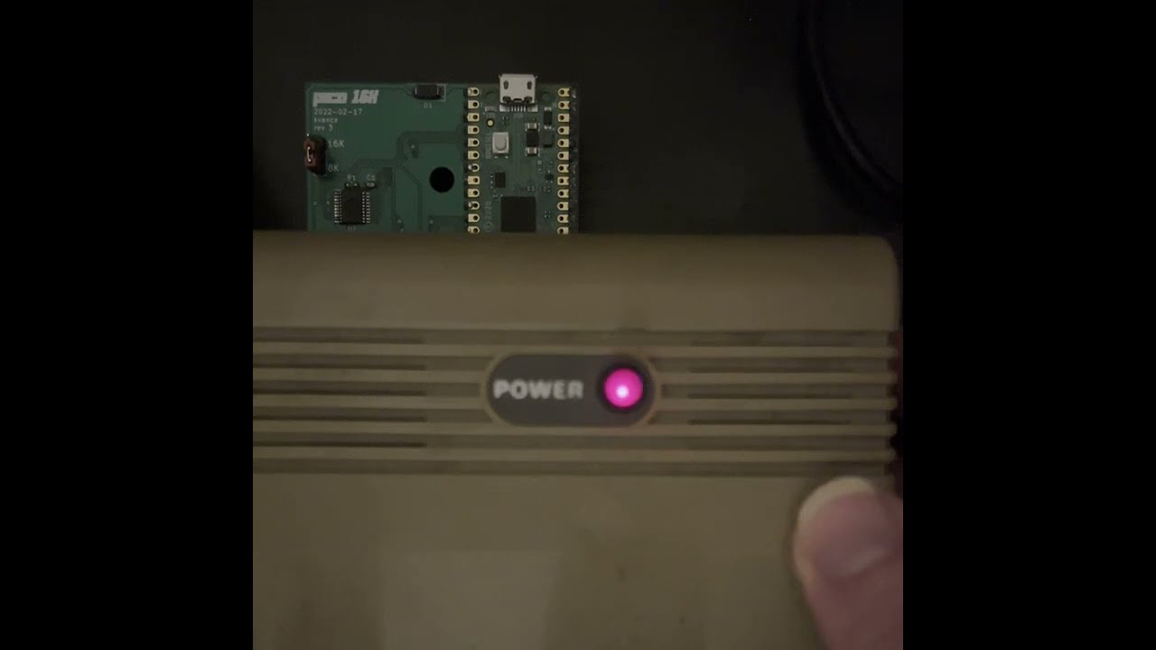 10 |
10 |