├── LICENSE
├── README.md
├── images
├── banner.png
├── image1.jpg
├── image2.jpg
├── image3.jpg
├── image4.jpg
├── image5.jpg
├── image6.jpg
├── image7.jpg
└── pci2nano.gif
├── pci2nano-cache.lib
├── pci2nano.kicad_pcb
├── pci2nano.net
├── pci2nano.pro
├── pci2nano.qpf
├── pci2nano.qsf
├── pci2nano.sch
└── pci2nano.v
/LICENSE:
--------------------------------------------------------------------------------
1 | Attribution-ShareAlike 4.0 International
2 |
3 | =======================================================================
4 |
5 | Creative Commons Corporation ("Creative Commons") is not a law firm and
6 | does not provide legal services or legal advice. Distribution of
7 | Creative Commons public licenses does not create a lawyer-client or
8 | other relationship. Creative Commons makes its licenses and related
9 | information available on an "as-is" basis. Creative Commons gives no
10 | warranties regarding its licenses, any material licensed under their
11 | terms and conditions, or any related information. Creative Commons
12 | disclaims all liability for damages resulting from their use to the
13 | fullest extent possible.
14 |
15 | Using Creative Commons Public Licenses
16 |
17 | Creative Commons public licenses provide a standard set of terms and
18 | conditions that creators and other rights holders may use to share
19 | original works of authorship and other material subject to copyright
20 | and certain other rights specified in the public license below. The
21 | following considerations are for informational purposes only, are not
22 | exhaustive, and do not form part of our licenses.
23 |
24 | Considerations for licensors: Our public licenses are
25 | intended for use by those authorized to give the public
26 | permission to use material in ways otherwise restricted by
27 | copyright and certain other rights. Our licenses are
28 | irrevocable. Licensors should read and understand the terms
29 | and conditions of the license they choose before applying it.
30 | Licensors should also secure all rights necessary before
31 | applying our licenses so that the public can reuse the
32 | material as expected. Licensors should clearly mark any
33 | material not subject to the license. This includes other CC-
34 | licensed material, or material used under an exception or
35 | limitation to copyright. More considerations for licensors:
36 | wiki.creativecommons.org/Considerations_for_licensors
37 |
38 | Considerations for the public: By using one of our public
39 | licenses, a licensor grants the public permission to use the
40 | licensed material under specified terms and conditions. If
41 | the licensor's permission is not necessary for any reason--for
42 | example, because of any applicable exception or limitation to
43 | copyright--then that use is not regulated by the license. Our
44 | licenses grant only permissions under copyright and certain
45 | other rights that a licensor has authority to grant. Use of
46 | the licensed material may still be restricted for other
47 | reasons, including because others have copyright or other
48 | rights in the material. A licensor may make special requests,
49 | such as asking that all changes be marked or described.
50 | Although not required by our licenses, you are encouraged to
51 | respect those requests where reasonable. More considerations
52 | for the public:
53 | wiki.creativecommons.org/Considerations_for_licensees
54 |
55 | =======================================================================
56 |
57 | Creative Commons Attribution-ShareAlike 4.0 International Public
58 | License
59 |
60 | By exercising the Licensed Rights (defined below), You accept and agree
61 | to be bound by the terms and conditions of this Creative Commons
62 | Attribution-ShareAlike 4.0 International Public License ("Public
63 | License"). To the extent this Public License may be interpreted as a
64 | contract, You are granted the Licensed Rights in consideration of Your
65 | acceptance of these terms and conditions, and the Licensor grants You
66 | such rights in consideration of benefits the Licensor receives from
67 | making the Licensed Material available under these terms and
68 | conditions.
69 |
70 |
71 | Section 1 -- Definitions.
72 |
73 | a. Adapted Material means material subject to Copyright and Similar
74 | Rights that is derived from or based upon the Licensed Material
75 | and in which the Licensed Material is translated, altered,
76 | arranged, transformed, or otherwise modified in a manner requiring
77 | permission under the Copyright and Similar Rights held by the
78 | Licensor. For purposes of this Public License, where the Licensed
79 | Material is a musical work, performance, or sound recording,
80 | Adapted Material is always produced where the Licensed Material is
81 | synched in timed relation with a moving image.
82 |
83 | b. Adapter's License means the license You apply to Your Copyright
84 | and Similar Rights in Your contributions to Adapted Material in
85 | accordance with the terms and conditions of this Public License.
86 |
87 | c. BY-SA Compatible License means a license listed at
88 | creativecommons.org/compatiblelicenses, approved by Creative
89 | Commons as essentially the equivalent of this Public License.
90 |
91 | d. Copyright and Similar Rights means copyright and/or similar rights
92 | closely related to copyright including, without limitation,
93 | performance, broadcast, sound recording, and Sui Generis Database
94 | Rights, without regard to how the rights are labeled or
95 | categorized. For purposes of this Public License, the rights
96 | specified in Section 2(b)(1)-(2) are not Copyright and Similar
97 | Rights.
98 |
99 | e. Effective Technological Measures means those measures that, in the
100 | absence of proper authority, may not be circumvented under laws
101 | fulfilling obligations under Article 11 of the WIPO Copyright
102 | Treaty adopted on December 20, 1996, and/or similar international
103 | agreements.
104 |
105 | f. Exceptions and Limitations means fair use, fair dealing, and/or
106 | any other exception or limitation to Copyright and Similar Rights
107 | that applies to Your use of the Licensed Material.
108 |
109 | g. License Elements means the license attributes listed in the name
110 | of a Creative Commons Public License. The License Elements of this
111 | Public License are Attribution and ShareAlike.
112 |
113 | h. Licensed Material means the artistic or literary work, database,
114 | or other material to which the Licensor applied this Public
115 | License.
116 |
117 | i. Licensed Rights means the rights granted to You subject to the
118 | terms and conditions of this Public License, which are limited to
119 | all Copyright and Similar Rights that apply to Your use of the
120 | Licensed Material and that the Licensor has authority to license.
121 |
122 | j. Licensor means the individual(s) or entity(ies) granting rights
123 | under this Public License.
124 |
125 | k. Share means to provide material to the public by any means or
126 | process that requires permission under the Licensed Rights, such
127 | as reproduction, public display, public performance, distribution,
128 | dissemination, communication, or importation, and to make material
129 | available to the public including in ways that members of the
130 | public may access the material from a place and at a time
131 | individually chosen by them.
132 |
133 | l. Sui Generis Database Rights means rights other than copyright
134 | resulting from Directive 96/9/EC of the European Parliament and of
135 | the Council of 11 March 1996 on the legal protection of databases,
136 | as amended and/or succeeded, as well as other essentially
137 | equivalent rights anywhere in the world.
138 |
139 | m. You means the individual or entity exercising the Licensed Rights
140 | under this Public License. Your has a corresponding meaning.
141 |
142 |
143 | Section 2 -- Scope.
144 |
145 | a. License grant.
146 |
147 | 1. Subject to the terms and conditions of this Public License,
148 | the Licensor hereby grants You a worldwide, royalty-free,
149 | non-sublicensable, non-exclusive, irrevocable license to
150 | exercise the Licensed Rights in the Licensed Material to:
151 |
152 | a. reproduce and Share the Licensed Material, in whole or
153 | in part; and
154 |
155 | b. produce, reproduce, and Share Adapted Material.
156 |
157 | 2. Exceptions and Limitations. For the avoidance of doubt, where
158 | Exceptions and Limitations apply to Your use, this Public
159 | License does not apply, and You do not need to comply with
160 | its terms and conditions.
161 |
162 | 3. Term. The term of this Public License is specified in Section
163 | 6(a).
164 |
165 | 4. Media and formats; technical modifications allowed. The
166 | Licensor authorizes You to exercise the Licensed Rights in
167 | all media and formats whether now known or hereafter created,
168 | and to make technical modifications necessary to do so. The
169 | Licensor waives and/or agrees not to assert any right or
170 | authority to forbid You from making technical modifications
171 | necessary to exercise the Licensed Rights, including
172 | technical modifications necessary to circumvent Effective
173 | Technological Measures. For purposes of this Public License,
174 | simply making modifications authorized by this Section 2(a)
175 | (4) never produces Adapted Material.
176 |
177 | 5. Downstream recipients.
178 |
179 | a. Offer from the Licensor -- Licensed Material. Every
180 | recipient of the Licensed Material automatically
181 | receives an offer from the Licensor to exercise the
182 | Licensed Rights under the terms and conditions of this
183 | Public License.
184 |
185 | b. Additional offer from the Licensor -- Adapted Material.
186 | Every recipient of Adapted Material from You
187 | automatically receives an offer from the Licensor to
188 | exercise the Licensed Rights in the Adapted Material
189 | under the conditions of the Adapter's License You apply.
190 |
191 | c. No downstream restrictions. You may not offer or impose
192 | any additional or different terms or conditions on, or
193 | apply any Effective Technological Measures to, the
194 | Licensed Material if doing so restricts exercise of the
195 | Licensed Rights by any recipient of the Licensed
196 | Material.
197 |
198 | 6. No endorsement. Nothing in this Public License constitutes or
199 | may be construed as permission to assert or imply that You
200 | are, or that Your use of the Licensed Material is, connected
201 | with, or sponsored, endorsed, or granted official status by,
202 | the Licensor or others designated to receive attribution as
203 | provided in Section 3(a)(1)(A)(i).
204 |
205 | b. Other rights.
206 |
207 | 1. Moral rights, such as the right of integrity, are not
208 | licensed under this Public License, nor are publicity,
209 | privacy, and/or other similar personality rights; however, to
210 | the extent possible, the Licensor waives and/or agrees not to
211 | assert any such rights held by the Licensor to the limited
212 | extent necessary to allow You to exercise the Licensed
213 | Rights, but not otherwise.
214 |
215 | 2. Patent and trademark rights are not licensed under this
216 | Public License.
217 |
218 | 3. To the extent possible, the Licensor waives any right to
219 | collect royalties from You for the exercise of the Licensed
220 | Rights, whether directly or through a collecting society
221 | under any voluntary or waivable statutory or compulsory
222 | licensing scheme. In all other cases the Licensor expressly
223 | reserves any right to collect such royalties.
224 |
225 |
226 | Section 3 -- License Conditions.
227 |
228 | Your exercise of the Licensed Rights is expressly made subject to the
229 | following conditions.
230 |
231 | a. Attribution.
232 |
233 | 1. If You Share the Licensed Material (including in modified
234 | form), You must:
235 |
236 | a. retain the following if it is supplied by the Licensor
237 | with the Licensed Material:
238 |
239 | i. identification of the creator(s) of the Licensed
240 | Material and any others designated to receive
241 | attribution, in any reasonable manner requested by
242 | the Licensor (including by pseudonym if
243 | designated);
244 |
245 | ii. a copyright notice;
246 |
247 | iii. a notice that refers to this Public License;
248 |
249 | iv. a notice that refers to the disclaimer of
250 | warranties;
251 |
252 | v. a URI or hyperlink to the Licensed Material to the
253 | extent reasonably practicable;
254 |
255 | b. indicate if You modified the Licensed Material and
256 | retain an indication of any previous modifications; and
257 |
258 | c. indicate the Licensed Material is licensed under this
259 | Public License, and include the text of, or the URI or
260 | hyperlink to, this Public License.
261 |
262 | 2. You may satisfy the conditions in Section 3(a)(1) in any
263 | reasonable manner based on the medium, means, and context in
264 | which You Share the Licensed Material. For example, it may be
265 | reasonable to satisfy the conditions by providing a URI or
266 | hyperlink to a resource that includes the required
267 | information.
268 |
269 | 3. If requested by the Licensor, You must remove any of the
270 | information required by Section 3(a)(1)(A) to the extent
271 | reasonably practicable.
272 |
273 | b. ShareAlike.
274 |
275 | In addition to the conditions in Section 3(a), if You Share
276 | Adapted Material You produce, the following conditions also apply.
277 |
278 | 1. The Adapter's License You apply must be a Creative Commons
279 | license with the same License Elements, this version or
280 | later, or a BY-SA Compatible License.
281 |
282 | 2. You must include the text of, or the URI or hyperlink to, the
283 | Adapter's License You apply. You may satisfy this condition
284 | in any reasonable manner based on the medium, means, and
285 | context in which You Share Adapted Material.
286 |
287 | 3. You may not offer or impose any additional or different terms
288 | or conditions on, or apply any Effective Technological
289 | Measures to, Adapted Material that restrict exercise of the
290 | rights granted under the Adapter's License You apply.
291 |
292 |
293 | Section 4 -- Sui Generis Database Rights.
294 |
295 | Where the Licensed Rights include Sui Generis Database Rights that
296 | apply to Your use of the Licensed Material:
297 |
298 | a. for the avoidance of doubt, Section 2(a)(1) grants You the right
299 | to extract, reuse, reproduce, and Share all or a substantial
300 | portion of the contents of the database;
301 |
302 | b. if You include all or a substantial portion of the database
303 | contents in a database in which You have Sui Generis Database
304 | Rights, then the database in which You have Sui Generis Database
305 | Rights (but not its individual contents) is Adapted Material,
306 |
307 | including for purposes of Section 3(b); and
308 | c. You must comply with the conditions in Section 3(a) if You Share
309 | all or a substantial portion of the contents of the database.
310 |
311 | For the avoidance of doubt, this Section 4 supplements and does not
312 | replace Your obligations under this Public License where the Licensed
313 | Rights include other Copyright and Similar Rights.
314 |
315 |
316 | Section 5 -- Disclaimer of Warranties and Limitation of Liability.
317 |
318 | a. UNLESS OTHERWISE SEPARATELY UNDERTAKEN BY THE LICENSOR, TO THE
319 | EXTENT POSSIBLE, THE LICENSOR OFFERS THE LICENSED MATERIAL AS-IS
320 | AND AS-AVAILABLE, AND MAKES NO REPRESENTATIONS OR WARRANTIES OF
321 | ANY KIND CONCERNING THE LICENSED MATERIAL, WHETHER EXPRESS,
322 | IMPLIED, STATUTORY, OR OTHER. THIS INCLUDES, WITHOUT LIMITATION,
323 | WARRANTIES OF TITLE, MERCHANTABILITY, FITNESS FOR A PARTICULAR
324 | PURPOSE, NON-INFRINGEMENT, ABSENCE OF LATENT OR OTHER DEFECTS,
325 | ACCURACY, OR THE PRESENCE OR ABSENCE OF ERRORS, WHETHER OR NOT
326 | KNOWN OR DISCOVERABLE. WHERE DISCLAIMERS OF WARRANTIES ARE NOT
327 | ALLOWED IN FULL OR IN PART, THIS DISCLAIMER MAY NOT APPLY TO YOU.
328 |
329 | b. TO THE EXTENT POSSIBLE, IN NO EVENT WILL THE LICENSOR BE LIABLE
330 | TO YOU ON ANY LEGAL THEORY (INCLUDING, WITHOUT LIMITATION,
331 | NEGLIGENCE) OR OTHERWISE FOR ANY DIRECT, SPECIAL, INDIRECT,
332 | INCIDENTAL, CONSEQUENTIAL, PUNITIVE, EXEMPLARY, OR OTHER LOSSES,
333 | COSTS, EXPENSES, OR DAMAGES ARISING OUT OF THIS PUBLIC LICENSE OR
334 | USE OF THE LICENSED MATERIAL, EVEN IF THE LICENSOR HAS BEEN
335 | ADVISED OF THE POSSIBILITY OF SUCH LOSSES, COSTS, EXPENSES, OR
336 | DAMAGES. WHERE A LIMITATION OF LIABILITY IS NOT ALLOWED IN FULL OR
337 | IN PART, THIS LIMITATION MAY NOT APPLY TO YOU.
338 |
339 | c. The disclaimer of warranties and limitation of liability provided
340 | above shall be interpreted in a manner that, to the extent
341 | possible, most closely approximates an absolute disclaimer and
342 | waiver of all liability.
343 |
344 |
345 | Section 6 -- Term and Termination.
346 |
347 | a. This Public License applies for the term of the Copyright and
348 | Similar Rights licensed here. However, if You fail to comply with
349 | this Public License, then Your rights under this Public License
350 | terminate automatically.
351 |
352 | b. Where Your right to use the Licensed Material has terminated under
353 | Section 6(a), it reinstates:
354 |
355 | 1. automatically as of the date the violation is cured, provided
356 | it is cured within 30 days of Your discovery of the
357 | violation; or
358 |
359 | 2. upon express reinstatement by the Licensor.
360 |
361 | For the avoidance of doubt, this Section 6(b) does not affect any
362 | right the Licensor may have to seek remedies for Your violations
363 | of this Public License.
364 |
365 | c. For the avoidance of doubt, the Licensor may also offer the
366 | Licensed Material under separate terms or conditions or stop
367 | distributing the Licensed Material at any time; however, doing so
368 | will not terminate this Public License.
369 |
370 | d. Sections 1, 5, 6, 7, and 8 survive termination of this Public
371 | License.
372 |
373 |
374 | Section 7 -- Other Terms and Conditions.
375 |
376 | a. The Licensor shall not be bound by any additional or different
377 | terms or conditions communicated by You unless expressly agreed.
378 |
379 | b. Any arrangements, understandings, or agreements regarding the
380 | Licensed Material not stated herein are separate from and
381 | independent of the terms and conditions of this Public License.
382 |
383 |
384 | Section 8 -- Interpretation.
385 |
386 | a. For the avoidance of doubt, this Public License does not, and
387 | shall not be interpreted to, reduce, limit, restrict, or impose
388 | conditions on any use of the Licensed Material that could lawfully
389 | be made without permission under this Public License.
390 |
391 | b. To the extent possible, if any provision of this Public License is
392 | deemed unenforceable, it shall be automatically reformed to the
393 | minimum extent necessary to make it enforceable. If the provision
394 | cannot be reformed, it shall be severed from this Public License
395 | without affecting the enforceability of the remaining terms and
396 | conditions.
397 |
398 | c. No term or condition of this Public License will be waived and no
399 | failure to comply consented to unless expressly agreed to by the
400 | Licensor.
401 |
402 | d. Nothing in this Public License constitutes or may be interpreted
403 | as a limitation upon, or waiver of, any privileges and immunities
404 | that apply to the Licensor or You, including from the legal
405 | processes of any jurisdiction or authority.
406 |
407 |
408 | =======================================================================
409 |
410 | Creative Commons is not a party to its public
411 | licenses. Notwithstanding, Creative Commons may elect to apply one of
412 | its public licenses to material it publishes and in those instances
413 | will be considered the “Licensor.” The text of the Creative Commons
414 | public licenses is dedicated to the public domain under the CC0 Public
415 | Domain Dedication. Except for the limited purpose of indicating that
416 | material is shared under a Creative Commons public license or as
417 | otherwise permitted by the Creative Commons policies published at
418 | creativecommons.org/policies, Creative Commons does not authorize the
419 | use of the trademark "Creative Commons" or any other trademark or logo
420 | of Creative Commons without its prior written consent including,
421 | without limitation, in connection with any unauthorized modifications
422 | to any of its public licenses or any other arrangements,
423 | understandings, or agreements concerning use of licensed material. For
424 | the avoidance of doubt, this paragraph does not form part of the
425 | public licenses.
426 |
427 | Creative Commons may be contacted at creativecommons.org.
428 |
--------------------------------------------------------------------------------
/README.md:
--------------------------------------------------------------------------------
1 | # PCI2Nano Reference Platform
2 |
3 | 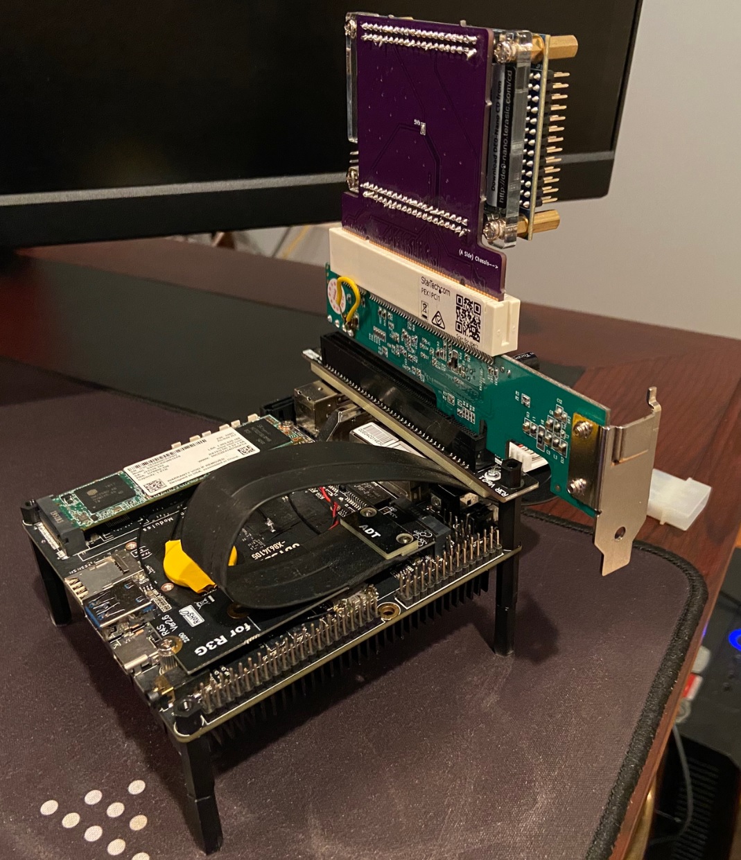 4 |
5 | Welcome to the PCI2Nano Reference Platform repo. In this repo you'll find an inexpensive suggested Reference Platform for designing and testing PCI functions on a DE0-Nano FPGA to an x86 host. I have personally built/connected/tested every single one of these components and can confirm they work for fast iterative PCI development.
6 |
7 | The design collateral that is included with this repo are the kicad design files for the PCI2Nano breakout board and a Quartus project that contains all the correct PCI pinout constraints for the PCI2Nano breakout board. This repo does not contain an actual PCI core written in verilog. For an example PCI core implementation with a UART check out the PCI2Nano-RTL repo here: https://github.com/defparam/PCI2Nano-RTL/
8 |
9 |
4 |
5 | Welcome to the PCI2Nano Reference Platform repo. In this repo you'll find an inexpensive suggested Reference Platform for designing and testing PCI functions on a DE0-Nano FPGA to an x86 host. I have personally built/connected/tested every single one of these components and can confirm they work for fast iterative PCI development.
6 |
7 | The design collateral that is included with this repo are the kicad design files for the PCI2Nano breakout board and a Quartus project that contains all the correct PCI pinout constraints for the PCI2Nano breakout board. This repo does not contain an actual PCI core written in verilog. For an example PCI core implementation with a UART check out the PCI2Nano-RTL repo here: https://github.com/defparam/PCI2Nano-RTL/
8 |
9 | 
This work is licensed under a Creative Commons Attribution-ShareAlike 4.0 International License.
10 |
11 | # Demo
12 | My l337-Communication Controller
13 |
14 | 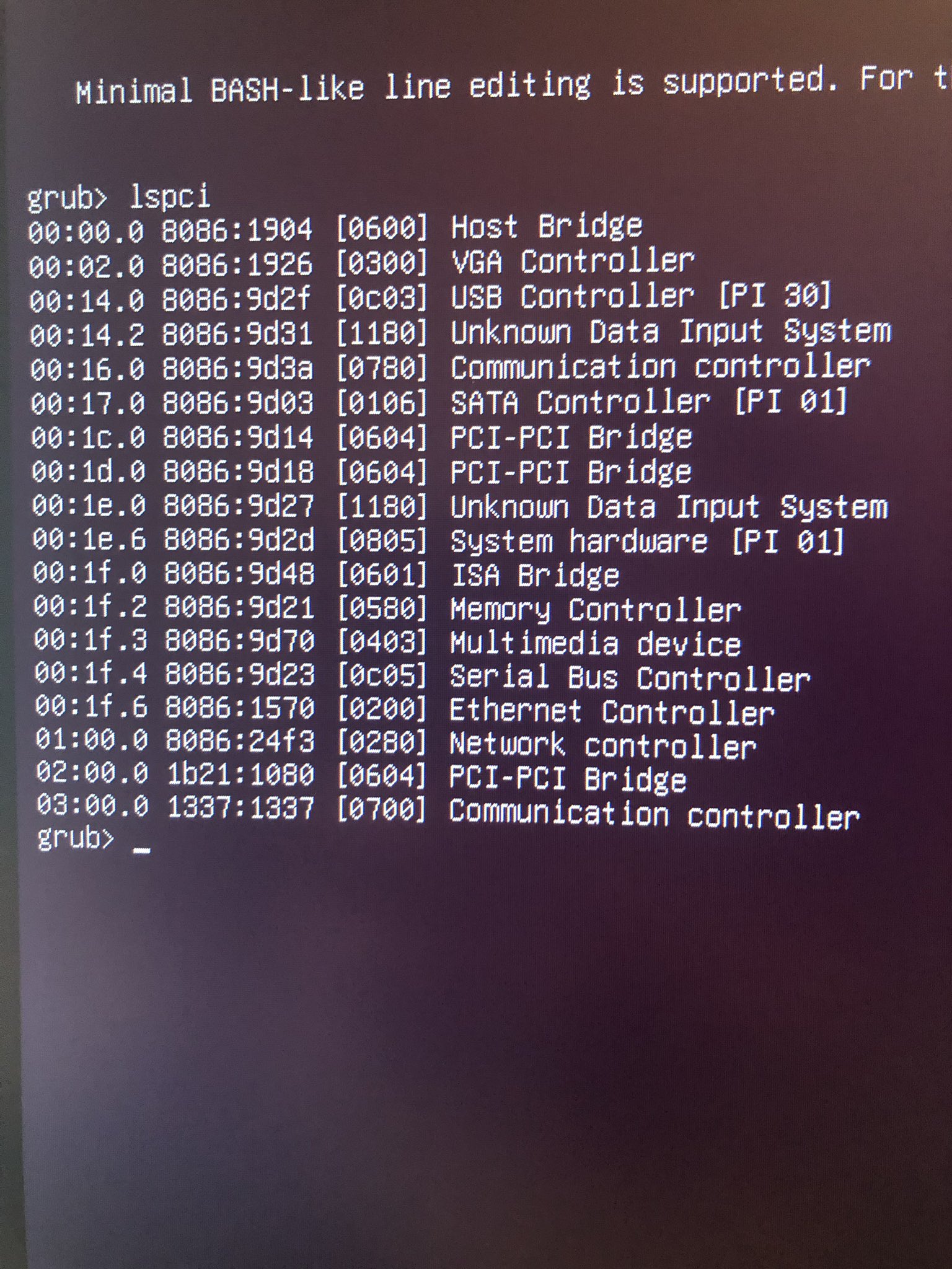 15 |
16 | # Reference Platform Parts List
17 | | Part | Description| Price |
18 | |--|--|--|
19 | | DE0-Nano | FPGA Board|~$100.00
20 | | Seeed Odyssey X86J4105 SBC | SIngle Board Computer | ~$185.00
21 | |PCI2Nano Breakout PCB|Coverts PCI to DE0-Nano GPIO | ~$45 (OSHPark for 3)
22 | |Startech PEX1PCI1| Converts PCIe to PCI | ~$40
23 | |M.2 Key M Extender PCIE x16 | Break out M.2 to PCIe x16 | ~$32
24 | 2x 100mil 40-pin IDC sockets| Soldered to the PCB| ~$1-$2
25 |
26 | # Directions
27 | 1) Mount the Extender cable into the Odyssey M.2 M Key slot. If you have standoffs you can affix the x16 connector of the extender to the SBC as shown in the picture above.
28 | 2) Mount the PEX1PCI1 onto the x16 connector. Supplying the molex power I believe is not required since it is used to power the 5V rails of a mounted PCI device, the PCI2Nano doesn't use this 5V rail (unless you bridge it to the Nano's 5V GPIO power pin via the board shunt). However it is best to power the nano through its USB cable
29 | 3) Connect the PCI2Nano breakout board to the DE0-Nano, make sure that the USB of the nano points in the correct direction as specified by the silkscreen
30 | 4) Connect the PCI side of the PCI2Nano onto the PEX1PCI1, make sure it is connected in the orientation as indicated by the silk screen. The arrow indicating the chassis side should be pointed to the externel side of the PEX1PCI1
31 |
32 | # PCB board
33 | There is a small amount of soldering involved with the PCB board to connect the 100mil IDC socket to the PCB board.
34 |
35 | # Parts
36 | The DE0-Nano:
37 |
38 |
15 |
16 | # Reference Platform Parts List
17 | | Part | Description| Price |
18 | |--|--|--|
19 | | DE0-Nano | FPGA Board|~$100.00
20 | | Seeed Odyssey X86J4105 SBC | SIngle Board Computer | ~$185.00
21 | |PCI2Nano Breakout PCB|Coverts PCI to DE0-Nano GPIO | ~$45 (OSHPark for 3)
22 | |Startech PEX1PCI1| Converts PCIe to PCI | ~$40
23 | |M.2 Key M Extender PCIE x16 | Break out M.2 to PCIe x16 | ~$32
24 | 2x 100mil 40-pin IDC sockets| Soldered to the PCB| ~$1-$2
25 |
26 | # Directions
27 | 1) Mount the Extender cable into the Odyssey M.2 M Key slot. If you have standoffs you can affix the x16 connector of the extender to the SBC as shown in the picture above.
28 | 2) Mount the PEX1PCI1 onto the x16 connector. Supplying the molex power I believe is not required since it is used to power the 5V rails of a mounted PCI device, the PCI2Nano doesn't use this 5V rail (unless you bridge it to the Nano's 5V GPIO power pin via the board shunt). However it is best to power the nano through its USB cable
29 | 3) Connect the PCI2Nano breakout board to the DE0-Nano, make sure that the USB of the nano points in the correct direction as specified by the silkscreen
30 | 4) Connect the PCI side of the PCI2Nano onto the PEX1PCI1, make sure it is connected in the orientation as indicated by the silk screen. The arrow indicating the chassis side should be pointed to the externel side of the PEX1PCI1
31 |
32 | # PCB board
33 | There is a small amount of soldering involved with the PCB board to connect the 100mil IDC socket to the PCB board.
34 |
35 | # Parts
36 | The DE0-Nano:
37 |
38 | 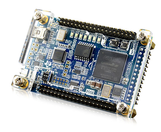 39 |
40 | The PCI2Nano PCB:
41 |
42 |
39 |
40 | The PCI2Nano PCB:
41 |
42 | 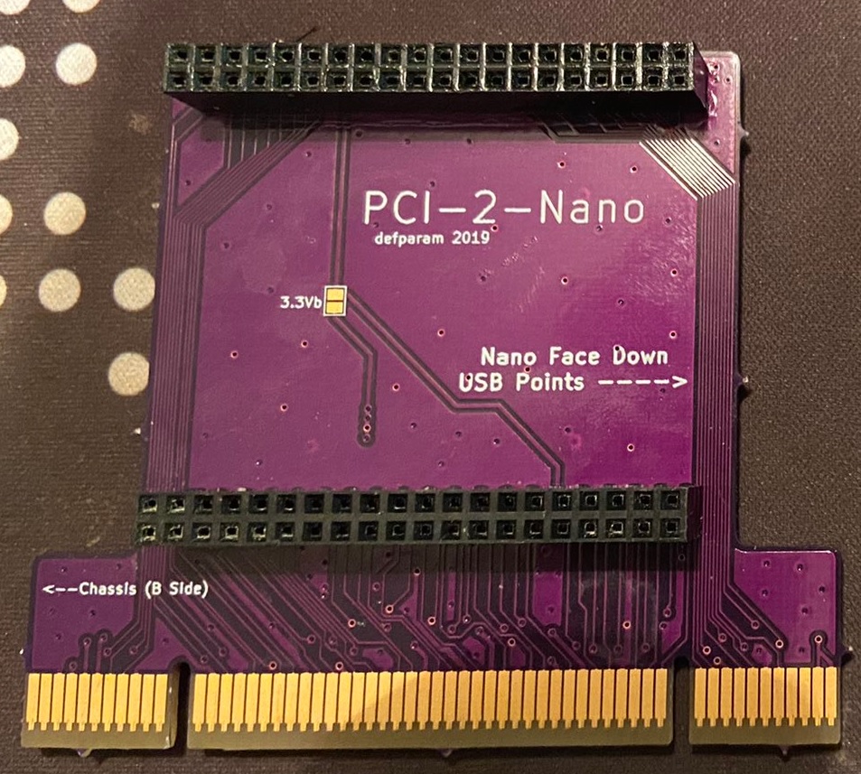 43 |
44 | The PEX1PCI1 PCIe-2-PCI Bridge:
45 |
46 |
43 |
44 | The PEX1PCI1 PCIe-2-PCI Bridge:
45 |
46 | 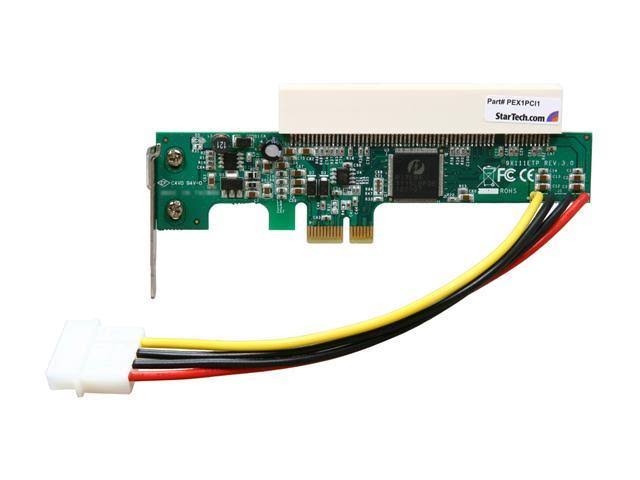 47 |
48 | The Seeed Odyssey X86J4105 SBC:
49 |
50 |
47 |
48 | The Seeed Odyssey X86J4105 SBC:
49 |
50 | 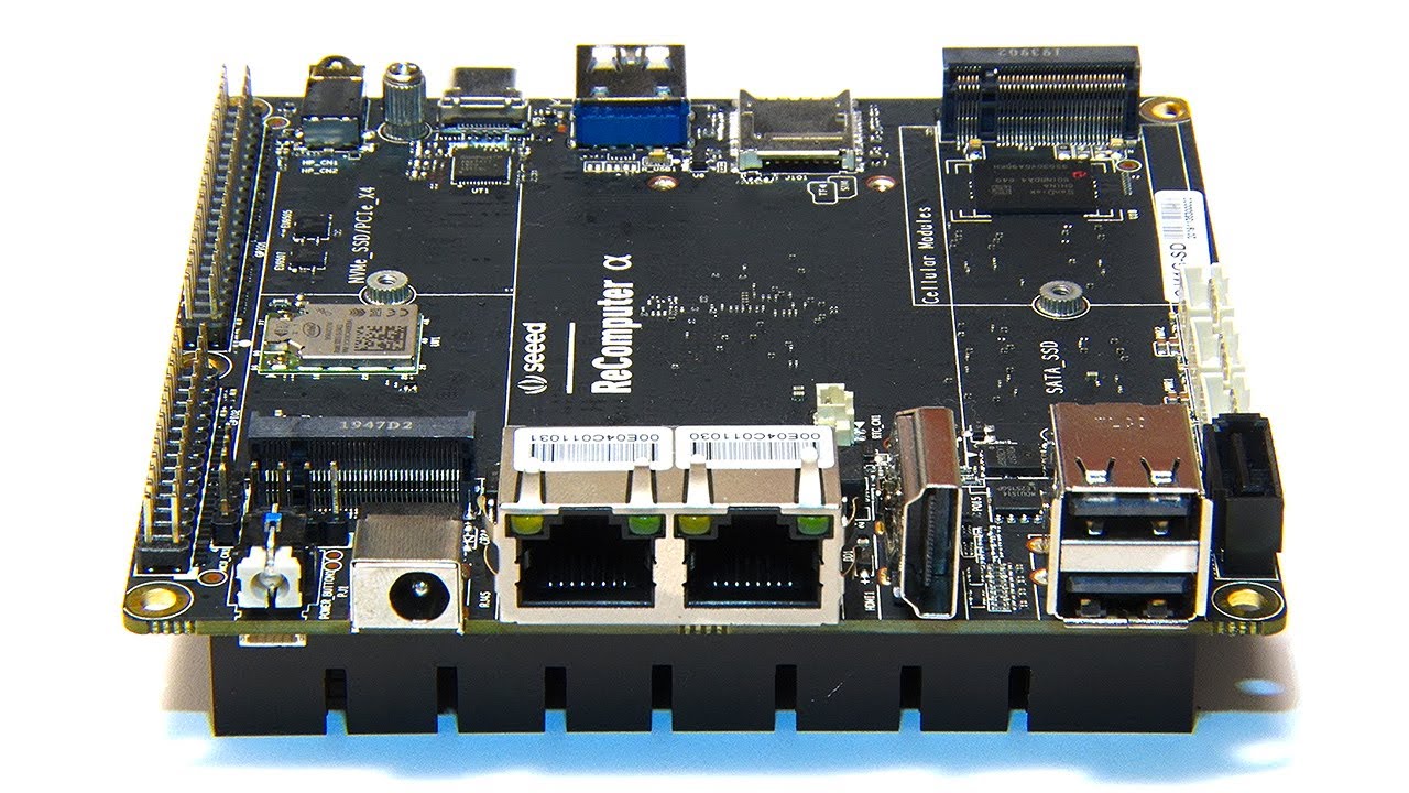 51 |
52 | The M.2 Key M Extender PCIE x16:
53 |
54 |
51 |
52 | The M.2 Key M Extender PCIE x16:
53 |
54 | 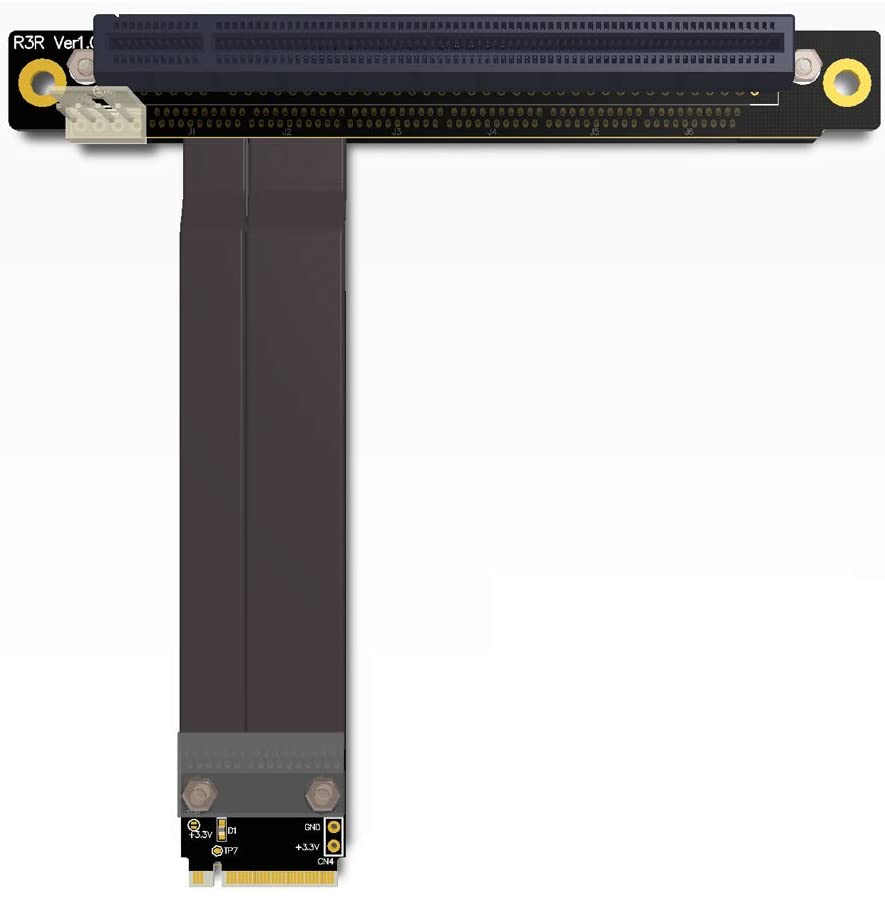 55 |
--------------------------------------------------------------------------------
/images/banner.png:
--------------------------------------------------------------------------------
https://raw.githubusercontent.com/defparam/PCI2Nano-PCB/c89a77f80c4dcbdea98dd997ebcd0e0f8f43258a/images/banner.png
--------------------------------------------------------------------------------
/images/image1.jpg:
--------------------------------------------------------------------------------
https://raw.githubusercontent.com/defparam/PCI2Nano-PCB/c89a77f80c4dcbdea98dd997ebcd0e0f8f43258a/images/image1.jpg
--------------------------------------------------------------------------------
/images/image2.jpg:
--------------------------------------------------------------------------------
https://raw.githubusercontent.com/defparam/PCI2Nano-PCB/c89a77f80c4dcbdea98dd997ebcd0e0f8f43258a/images/image2.jpg
--------------------------------------------------------------------------------
/images/image3.jpg:
--------------------------------------------------------------------------------
https://raw.githubusercontent.com/defparam/PCI2Nano-PCB/c89a77f80c4dcbdea98dd997ebcd0e0f8f43258a/images/image3.jpg
--------------------------------------------------------------------------------
/images/image4.jpg:
--------------------------------------------------------------------------------
https://raw.githubusercontent.com/defparam/PCI2Nano-PCB/c89a77f80c4dcbdea98dd997ebcd0e0f8f43258a/images/image4.jpg
--------------------------------------------------------------------------------
/images/image5.jpg:
--------------------------------------------------------------------------------
https://raw.githubusercontent.com/defparam/PCI2Nano-PCB/c89a77f80c4dcbdea98dd997ebcd0e0f8f43258a/images/image5.jpg
--------------------------------------------------------------------------------
/images/image6.jpg:
--------------------------------------------------------------------------------
https://raw.githubusercontent.com/defparam/PCI2Nano-PCB/c89a77f80c4dcbdea98dd997ebcd0e0f8f43258a/images/image6.jpg
--------------------------------------------------------------------------------
/images/image7.jpg:
--------------------------------------------------------------------------------
https://raw.githubusercontent.com/defparam/PCI2Nano-PCB/c89a77f80c4dcbdea98dd997ebcd0e0f8f43258a/images/image7.jpg
--------------------------------------------------------------------------------
/images/pci2nano.gif:
--------------------------------------------------------------------------------
https://raw.githubusercontent.com/defparam/PCI2Nano-PCB/c89a77f80c4dcbdea98dd997ebcd0e0f8f43258a/images/pci2nano.gif
--------------------------------------------------------------------------------
/pci2nano-cache.lib:
--------------------------------------------------------------------------------
1 | EESchema-LIBRARY Version 2.4
2 | #encoding utf-8
3 | #
4 | # Connector_Bus_PCI_32bit_Universal
5 | #
6 | DEF Connector_Bus_PCI_32bit_Universal J 0 20 Y Y 1 F N
7 | F0 "J" 0 3150 50 H V C CNN
8 | F1 "Connector_Bus_PCI_32bit_Universal" 0 -3250 50 H V C CNN
9 | F2 "" 0 -50 50 H I C CNN
10 | F3 "" 0 -50 50 H I C CNN
11 | DRAW
12 | S -750 3100 750 -3200 0 1 10 f
13 | X ~TRST# A1 900 3000 150 L 50 50 1 1 O
14 | X VIO A10 900 2100 150 L 50 50 1 1 W
15 | X RESERVED A11 900 2000 150 L 50 50 1 1 P
16 | X 3.3VAUX A14 900 1700 150 L 50 50 1 1 P
17 | X ~RST# A15 900 1600 150 L 50 50 1 1 O
18 | X VIO A16 900 1500 150 L 50 50 1 1 W
19 | X ~GNT# A17 900 1400 150 L 50 50 1 1 B
20 | X GND A18 900 1300 150 L 50 50 1 1 W
21 | X PME# A19 900 1200 150 L 50 50 1 1 P
22 | X +12V A2 900 2900 150 L 50 50 1 1 W
23 | X AD[30] A20 900 1100 150 L 50 50 1 1 B
24 | X +3.3V A21 900 1000 150 L 50 50 1 1 W
25 | X AD[28] A22 900 900 150 L 50 50 1 1 B
26 | X AD[26] A23 900 800 150 L 50 50 1 1 B
27 | X GND A24 900 700 150 L 50 50 1 1 W
28 | X AD[24] A25 900 600 150 L 50 50 1 1 B
29 | X IDSEL A26 900 500 150 L 50 50 1 1 O
30 | X +3.3V A27 900 400 150 L 50 50 1 1 W
31 | X AD[22] A28 900 300 150 L 50 50 1 1 B
32 | X AD[20] A29 900 200 150 L 50 50 1 1 B
33 | X TMS A3 900 2800 150 L 50 50 1 1 O
34 | X GND A30 900 100 150 L 50 50 1 1 W
35 | X AD[18] A31 900 0 150 L 50 50 1 1 B
36 | X AD[16] A32 900 -100 150 L 50 50 1 1 B
37 | X +3.3V A33 900 -200 150 L 50 50 1 1 W
38 | X ~FRAME# A34 900 -300 150 L 50 50 1 1 B
39 | X GND A35 900 -400 150 L 50 50 1 1 W
40 | X ~TRDY# A36 900 -500 150 L 50 50 1 1 B
41 | X GND A37 900 -600 150 L 50 50 1 1 W
42 | X ~STOP# A38 900 -700 150 L 50 50 1 1 B
43 | X +3.3V A39 900 -800 150 L 50 50 1 1 W
44 | X TDI A4 900 2700 150 L 50 50 1 1 O
45 | X RESERVED A40 900 -900 150 L 50 50 1 1 B
46 | X RESERVED A41 900 -1000 150 L 50 50 1 1 B
47 | X GND A42 900 -1100 150 L 50 50 1 1 W
48 | X PAR A43 900 -1200 150 L 50 50 1 1 B
49 | X AD[15] A44 900 -1300 150 L 50 50 1 1 B
50 | X +3.3V A45 900 -1400 150 L 50 50 1 1 W
51 | X AD[13] A46 900 -1500 150 L 50 50 1 1 B
52 | X AD[11] A47 900 -1600 150 L 50 50 1 1 B
53 | X GND A48 900 -1700 150 L 50 50 1 1 W
54 | X AD[09] A49 900 -1800 150 L 50 50 1 1 B
55 | X +5V A5 900 2600 150 L 50 50 1 1 W
56 | X ~C/BE#[0] A52 900 -2100 150 L 50 50 1 1 B
57 | X +3.3V A53 900 -2200 150 L 50 50 1 1 W
58 | X AD[06] A54 900 -2300 150 L 50 50 1 1 B
59 | X AD[04] A55 900 -2400 150 L 50 50 1 1 B
60 | X GND A56 900 -2500 150 L 50 50 1 1 W
61 | X AD[02] A57 900 -2600 150 L 50 50 1 1 B
62 | X AD[00] A58 900 -2700 150 L 50 50 1 1 B
63 | X VIO A59 900 -2800 150 L 50 50 1 1 W
64 | X ~INTA# A6 900 2500 150 L 50 50 1 1 I
65 | X ~REQ64# A60 900 -2900 150 L 50 50 1 1 B
66 | X +5V A61 900 -3000 150 L 50 50 1 1 W
67 | X +5V A62 900 -3100 150 L 50 50 1 1 W
68 | X ~INTC# A7 900 2400 150 L 50 50 1 1 I
69 | X +5V A8 900 2300 150 L 50 50 1 1 W
70 | X RESERVED A9 900 2200 150 L 50 50 1 1 P
71 | X -12V B1 -900 3000 150 R 50 50 1 1 W
72 | X RESERVED B10 -900 2100 150 R 50 50 1 1 P
73 | X ~PRSNT2# B11 -900 2000 150 R 50 50 1 1 I
74 | X RESERVED B14 -900 1700 150 R 50 50 1 1 P
75 | X GND B15 -900 1600 150 R 50 50 1 1 W
76 | X CLK B16 -900 1500 150 R 50 50 1 1 O
77 | X GND B17 -900 1400 150 R 50 50 1 1 W
78 | X ~REQ# B18 -900 1300 150 R 50 50 1 1 B
79 | X VIO B19 -900 1200 150 R 50 50 1 1 W
80 | X TCK B2 -900 2900 150 R 50 50 1 1 O
81 | X AD[31] B20 -900 1100 150 R 50 50 1 1 B
82 | X AD[29] B21 -900 1000 150 R 50 50 1 1 B
83 | X GND B22 -900 900 150 R 50 50 1 1 W
84 | X AD[27] B23 -900 800 150 R 50 50 1 1 B
85 | X AD[25] B24 -900 700 150 R 50 50 1 1 B
86 | X +3.3V B25 -900 600 150 R 50 50 1 1 W
87 | X C/BE#[3] B26 -900 500 150 R 50 50 1 1 B
88 | X AD[23] B27 -900 400 150 R 50 50 1 1 B
89 | X GND B28 -900 300 150 R 50 50 1 1 W
90 | X AD[21] B29 -900 200 150 R 50 50 1 1 B
91 | X GND B3 -900 2800 150 R 50 50 1 1 W
92 | X AD[19] B30 -900 100 150 R 50 50 1 1 B
93 | X +3.3V B31 -900 0 150 R 50 50 1 1 W
94 | X AD[17] B32 -900 -100 150 R 50 50 1 1 B
95 | X ~C/BE#[2] B33 -900 -200 150 R 50 50 1 1 B
96 | X GND B34 -900 -300 150 R 50 50 1 1 W
97 | X ~IRDY# B35 -900 -400 150 R 50 50 1 1 B
98 | X +3.3V B36 -900 -500 150 R 50 50 1 1 W
99 | X ~DEVSEL# B37 -900 -600 150 R 50 50 1 1 B
100 | X GND B38 -900 -700 150 R 50 50 1 1 W
101 | X ~LOCK# B39 -900 -800 150 R 50 50 1 1 B
102 | X TDO B4 -900 2700 150 R 50 50 1 1 I
103 | X ~PERR# B40 -900 -900 150 R 50 50 1 1 B
104 | X +3.3V B41 -900 -1000 150 R 50 50 1 1 W
105 | X ~SERR# B42 -900 -1100 150 R 50 50 1 1 I
106 | X +3.3V B43 -900 -1200 150 R 50 50 1 1 W
107 | X ~C/BE#[1] B44 -900 -1300 150 R 50 50 1 1 B
108 | X AD[14] B45 -900 -1400 150 R 50 50 1 1 B
109 | X GND B46 -900 -1500 150 R 50 50 1 1 W
110 | X AD[12] B47 -900 -1600 150 R 50 50 1 1 B
111 | X AD[10] B48 -900 -1700 150 R 50 50 1 1 B
112 | X M66EN B49 -900 -1800 150 R 50 50 1 1 W
113 | X +5V B5 -900 2600 150 R 50 50 1 1 W
114 | X AD[08] B52 -900 -2100 150 R 50 50 1 1 B
115 | X AD[07] B53 -900 -2200 150 R 50 50 1 1 B
116 | X +3.3V B54 -900 -2300 150 R 50 50 1 1 I
117 | X AD[05] B55 -900 -2400 150 R 50 50 1 1 B
118 | X AD[03] B56 -900 -2500 150 R 50 50 1 1 B
119 | X GND B57 -900 -2600 150 R 50 50 1 1 W
120 | X AD[01] B58 -900 -2700 150 R 50 50 1 1 B
121 | X VIO B59 -900 -2800 150 R 50 50 1 1 W
122 | X +5V B6 -900 2500 150 R 50 50 1 1 W
123 | X ~ACK64# B60 -900 -2900 150 R 50 50 1 1 B
124 | X +5V B61 -900 -3000 150 R 50 50 1 1 W
125 | X +5V B62 -900 -3100 150 R 50 50 1 1 W
126 | X ~INTB# B7 -900 2400 150 R 50 50 1 1 I
127 | X ~INTD# B8 -900 2300 150 R 50 50 1 1 I
128 | X ~PRSNT1# B9 -900 2200 150 R 50 50 1 1 I
129 | ENDDRAW
130 | ENDDEF
131 | #
132 | # Connector_Generic_Conn_02x20_Odd_Even
133 | #
134 | DEF Connector_Generic_Conn_02x20_Odd_Even J 0 40 Y N 1 F N
135 | F0 "J" 50 1000 50 H V C CNN
136 | F1 "Connector_Generic_Conn_02x20_Odd_Even" 50 -1100 50 H V C CNN
137 | F2 "" 0 0 50 H I C CNN
138 | F3 "" 0 0 50 H I C CNN
139 | $FPLIST
140 | Connector*:*_2x??_*
141 | $ENDFPLIST
142 | DRAW
143 | S -50 -995 0 -1005 1 1 6 N
144 | S -50 -895 0 -905 1 1 6 N
145 | S -50 -795 0 -805 1 1 6 N
146 | S -50 -695 0 -705 1 1 6 N
147 | S -50 -595 0 -605 1 1 6 N
148 | S -50 -495 0 -505 1 1 6 N
149 | S -50 -395 0 -405 1 1 6 N
150 | S -50 -295 0 -305 1 1 6 N
151 | S -50 -195 0 -205 1 1 6 N
152 | S -50 -95 0 -105 1 1 6 N
153 | S -50 5 0 -5 1 1 6 N
154 | S -50 105 0 95 1 1 6 N
155 | S -50 205 0 195 1 1 6 N
156 | S -50 305 0 295 1 1 6 N
157 | S -50 405 0 395 1 1 6 N
158 | S -50 505 0 495 1 1 6 N
159 | S -50 605 0 595 1 1 6 N
160 | S -50 705 0 695 1 1 6 N
161 | S -50 805 0 795 1 1 6 N
162 | S -50 905 0 895 1 1 6 N
163 | S -50 950 150 -1050 1 1 10 f
164 | S 150 -995 100 -1005 1 1 6 N
165 | S 150 -895 100 -905 1 1 6 N
166 | S 150 -795 100 -805 1 1 6 N
167 | S 150 -695 100 -705 1 1 6 N
168 | S 150 -595 100 -605 1 1 6 N
169 | S 150 -495 100 -505 1 1 6 N
170 | S 150 -395 100 -405 1 1 6 N
171 | S 150 -295 100 -305 1 1 6 N
172 | S 150 -195 100 -205 1 1 6 N
173 | S 150 -95 100 -105 1 1 6 N
174 | S 150 5 100 -5 1 1 6 N
175 | S 150 105 100 95 1 1 6 N
176 | S 150 205 100 195 1 1 6 N
177 | S 150 305 100 295 1 1 6 N
178 | S 150 405 100 395 1 1 6 N
179 | S 150 505 100 495 1 1 6 N
180 | S 150 605 100 595 1 1 6 N
181 | S 150 705 100 695 1 1 6 N
182 | S 150 805 100 795 1 1 6 N
183 | S 150 905 100 895 1 1 6 N
184 | X Pin_1 1 -200 900 150 R 50 50 1 1 P
185 | X Pin_10 10 300 500 150 L 50 50 1 1 P
186 | X Pin_11 11 -200 400 150 R 50 50 1 1 P
187 | X Pin_12 12 300 400 150 L 50 50 1 1 P
188 | X Pin_13 13 -200 300 150 R 50 50 1 1 P
189 | X Pin_14 14 300 300 150 L 50 50 1 1 P
190 | X Pin_15 15 -200 200 150 R 50 50 1 1 P
191 | X Pin_16 16 300 200 150 L 50 50 1 1 P
192 | X Pin_17 17 -200 100 150 R 50 50 1 1 P
193 | X Pin_18 18 300 100 150 L 50 50 1 1 P
194 | X Pin_19 19 -200 0 150 R 50 50 1 1 P
195 | X Pin_2 2 300 900 150 L 50 50 1 1 P
196 | X Pin_20 20 300 0 150 L 50 50 1 1 P
197 | X Pin_21 21 -200 -100 150 R 50 50 1 1 P
198 | X Pin_22 22 300 -100 150 L 50 50 1 1 P
199 | X Pin_23 23 -200 -200 150 R 50 50 1 1 P
200 | X Pin_24 24 300 -200 150 L 50 50 1 1 P
201 | X Pin_25 25 -200 -300 150 R 50 50 1 1 P
202 | X Pin_26 26 300 -300 150 L 50 50 1 1 P
203 | X Pin_27 27 -200 -400 150 R 50 50 1 1 P
204 | X Pin_28 28 300 -400 150 L 50 50 1 1 P
205 | X Pin_29 29 -200 -500 150 R 50 50 1 1 P
206 | X Pin_3 3 -200 800 150 R 50 50 1 1 P
207 | X Pin_30 30 300 -500 150 L 50 50 1 1 P
208 | X Pin_31 31 -200 -600 150 R 50 50 1 1 P
209 | X Pin_32 32 300 -600 150 L 50 50 1 1 P
210 | X Pin_33 33 -200 -700 150 R 50 50 1 1 P
211 | X Pin_34 34 300 -700 150 L 50 50 1 1 P
212 | X Pin_35 35 -200 -800 150 R 50 50 1 1 P
213 | X Pin_36 36 300 -800 150 L 50 50 1 1 P
214 | X Pin_37 37 -200 -900 150 R 50 50 1 1 P
215 | X Pin_38 38 300 -900 150 L 50 50 1 1 P
216 | X Pin_39 39 -200 -1000 150 R 50 50 1 1 P
217 | X Pin_4 4 300 800 150 L 50 50 1 1 P
218 | X Pin_40 40 300 -1000 150 L 50 50 1 1 P
219 | X Pin_5 5 -200 700 150 R 50 50 1 1 P
220 | X Pin_6 6 300 700 150 L 50 50 1 1 P
221 | X Pin_7 7 -200 600 150 R 50 50 1 1 P
222 | X Pin_8 8 300 600 150 L 50 50 1 1 P
223 | X Pin_9 9 -200 500 150 R 50 50 1 1 P
224 | ENDDRAW
225 | ENDDEF
226 | #
227 | # Jumper_SolderJumper_2_Bridged
228 | #
229 | DEF Jumper_SolderJumper_2_Bridged JP 0 0 Y N 1 F N
230 | F0 "JP" 0 80 50 H V C CNN
231 | F1 "Jumper_SolderJumper_2_Bridged" 0 -100 50 H V C CNN
232 | F2 "" 0 0 50 H I C CNN
233 | F3 "" 0 0 50 H I C CNN
234 | $FPLIST
235 | SolderJumper*Bridged*
236 | $ENDFPLIST
237 | DRAW
238 | A -10 0 40 901 -901 0 1 0 N -10 40 -10 -40
239 | A -10 0 40 901 -901 0 1 0 F -10 40 -10 -40
240 | A 10 0 40 -899 899 0 1 0 N 10 -40 10 40
241 | A 10 0 40 -899 899 0 1 0 F 10 -40 10 40
242 | S -20 20 20 -20 0 1 0 F
243 | P 2 0 1 0 -10 40 -10 -40 N
244 | P 2 0 1 0 10 40 10 -40 N
245 | X A 1 -150 0 100 R 50 50 1 1 P
246 | X B 2 150 0 100 L 50 50 1 1 P
247 | ENDDRAW
248 | ENDDEF
249 | #
250 | # power_+3.3V
251 | #
252 | DEF power_+3.3V #PWR 0 0 Y Y 1 F P
253 | F0 "#PWR" 0 -150 50 H I C CNN
254 | F1 "power_+3.3V" 0 140 50 H V C CNN
255 | F2 "" 0 0 50 H I C CNN
256 | F3 "" 0 0 50 H I C CNN
257 | ALIAS +3.3V
258 | DRAW
259 | P 2 0 1 0 -30 50 0 100 N
260 | P 2 0 1 0 0 0 0 100 N
261 | P 2 0 1 0 0 100 30 50 N
262 | X +3V3 1 0 0 0 U 50 50 1 1 W N
263 | ENDDRAW
264 | ENDDEF
265 | #
266 | # power_+3.3VA
267 | #
268 | DEF power_+3.3VA #PWR 0 0 Y Y 1 F P
269 | F0 "#PWR" 0 -150 50 H I C CNN
270 | F1 "power_+3.3VA" 0 140 50 H V C CNN
271 | F2 "" 0 0 50 H I C CNN
272 | F3 "" 0 0 50 H I C CNN
273 | DRAW
274 | P 2 0 1 0 -30 50 0 100 N
275 | P 2 0 1 0 0 0 0 100 N
276 | P 2 0 1 0 0 100 30 50 N
277 | X +3.3VA 1 0 0 0 U 50 50 1 1 W N
278 | ENDDRAW
279 | ENDDEF
280 | #
281 | # power_+5V
282 | #
283 | DEF power_+5V #PWR 0 0 Y Y 1 F P
284 | F0 "#PWR" 0 -150 50 H I C CNN
285 | F1 "power_+5V" 0 140 50 H V C CNN
286 | F2 "" 0 0 50 H I C CNN
287 | F3 "" 0 0 50 H I C CNN
288 | DRAW
289 | P 2 0 1 0 -30 50 0 100 N
290 | P 2 0 1 0 0 0 0 100 N
291 | P 2 0 1 0 0 100 30 50 N
292 | X +5V 1 0 0 0 U 50 50 1 1 W N
293 | ENDDRAW
294 | ENDDEF
295 | #
296 | # power_+5VP
297 | #
298 | DEF power_+5VP #PWR 0 0 Y Y 1 F P
299 | F0 "#PWR" 0 -150 50 H I C CNN
300 | F1 "power_+5VP" 0 140 50 H V C CNN
301 | F2 "" 0 0 50 H I C CNN
302 | F3 "" 0 0 50 H I C CNN
303 | DRAW
304 | P 2 0 1 0 -30 50 0 100 N
305 | P 2 0 1 0 0 0 0 100 N
306 | P 2 0 1 0 0 100 30 50 N
307 | X +5VP 1 0 0 0 U 50 50 1 1 W N
308 | ENDDRAW
309 | ENDDEF
310 | #
311 | # power_GND
312 | #
313 | DEF power_GND #PWR 0 0 Y Y 1 F P
314 | F0 "#PWR" 0 -250 50 H I C CNN
315 | F1 "power_GND" 0 -150 50 H V C CNN
316 | F2 "" 0 0 50 H I C CNN
317 | F3 "" 0 0 50 H I C CNN
318 | DRAW
319 | P 6 0 1 0 0 0 0 -50 50 -50 0 -100 -50 -50 0 -50 N
320 | X GND 1 0 0 0 D 50 50 1 1 W N
321 | ENDDRAW
322 | ENDDEF
323 | #
324 | #End Library
325 |
--------------------------------------------------------------------------------
/pci2nano.net:
--------------------------------------------------------------------------------
1 | (export (version D)
2 | (design
3 | (source D:\hardware\pcb\pci2nano\pci2nano.sch)
4 | (date "9/27/2019 9:53:51 AM")
5 | (tool "Eeschema (5.1.4)-1")
6 | (sheet (number 1) (name /) (tstamps /)
7 | (title_block
8 | (title)
9 | (company)
10 | (rev)
11 | (date)
12 | (source pci2nano.sch)
13 | (comment (number 1) (value ""))
14 | (comment (number 2) (value ""))
15 | (comment (number 3) (value ""))
16 | (comment (number 4) (value "")))))
17 | (components
18 | (comp (ref J2)
19 | (value Conn_02x20_Odd_Even)
20 | (footprint Connector_PinHeader_2.54mm:PinHeader_2x20_P2.54mm_Vertical)
21 | (datasheet ~)
22 | (libsource (lib Connector_Generic) (part Conn_02x20_Odd_Even) (description "Generic connector, double row, 02x20, odd/even pin numbering scheme (row 1 odd numbers, row 2 even numbers), script generated (kicad-library-utils/schlib/autogen/connector/)"))
23 | (sheetpath (names /) (tstamps /))
24 | (tstamp 5D8D1ED3))
25 | (comp (ref J3)
26 | (value Conn_02x20_Odd_Even)
27 | (footprint Connector_PinHeader_2.54mm:PinHeader_2x20_P2.54mm_Vertical)
28 | (datasheet ~)
29 | (libsource (lib Connector_Generic) (part Conn_02x20_Odd_Even) (description "Generic connector, double row, 02x20, odd/even pin numbering scheme (row 1 odd numbers, row 2 even numbers), script generated (kicad-library-utils/schlib/autogen/connector/)"))
30 | (sheetpath (names /) (tstamps /))
31 | (tstamp 5D8D490E))
32 | (comp (ref J1)
33 | (value Bus_PCI_32bit_Universal)
34 | (footprint Connector_PCBEdge:BUS_PCI_UNIVERSAL)
35 | (datasheet http://pinouts.ru/Slots/PCI_pinout.shtml)
36 | (libsource (lib Connector) (part Bus_PCI_32bit_Universal) (description "PCI bus connector for universal 5V/3.3V cards"))
37 | (sheetpath (names /) (tstamps /))
38 | (tstamp 5D8DE1B0))
39 | (comp (ref JP1)
40 | (value SolderJumper_2_Bridged)
41 | (datasheet ~)
42 | (libsource (lib Jumper) (part SolderJumper_2_Bridged) (description "Solder Jumper, 2-pole, closed/bridged"))
43 | (sheetpath (names /) (tstamps /))
44 | (tstamp 5D8F6E87))
45 | (comp (ref JP2)
46 | (value SolderJumper_2_Bridged)
47 | (datasheet ~)
48 | (libsource (lib Jumper) (part SolderJumper_2_Bridged) (description "Solder Jumper, 2-pole, closed/bridged"))
49 | (sheetpath (names /) (tstamps /))
50 | (tstamp 5D900D15)))
51 | (libparts
52 | (libpart (lib Connector) (part Bus_PCI_32bit_Universal)
53 | (description "PCI bus connector for universal 5V/3.3V cards")
54 | (docs http://pinouts.ru/Slots/PCI_pinout.shtml)
55 | (fields
56 | (field (name Reference) J)
57 | (field (name Value) Bus_PCI_32bit_Universal))
58 | (pins
59 | (pin (num A1) (name ~TRST#) (type output))
60 | (pin (num A2) (name +12V) (type power_in))
61 | (pin (num A3) (name TMS) (type output))
62 | (pin (num A4) (name TDI) (type output))
63 | (pin (num A5) (name +5V) (type power_in))
64 | (pin (num A6) (name ~INTA#) (type input))
65 | (pin (num A7) (name ~INTC#) (type input))
66 | (pin (num A8) (name +5V) (type power_in))
67 | (pin (num A9) (name RESERVED) (type passive))
68 | (pin (num A10) (name VIO) (type power_in))
69 | (pin (num A11) (name RESERVED) (type passive))
70 | (pin (num A14) (name 3.3VAUX) (type passive))
71 | (pin (num A15) (name ~RST#) (type output))
72 | (pin (num A16) (name VIO) (type power_in))
73 | (pin (num A17) (name ~GNT#) (type BiDi))
74 | (pin (num A18) (name GND) (type power_in))
75 | (pin (num A19) (name PME#) (type passive))
76 | (pin (num A20) (name AD[30]) (type BiDi))
77 | (pin (num A21) (name +3.3V) (type power_in))
78 | (pin (num A22) (name AD[28]) (type BiDi))
79 | (pin (num A23) (name AD[26]) (type BiDi))
80 | (pin (num A24) (name GND) (type power_in))
81 | (pin (num A25) (name AD[24]) (type BiDi))
82 | (pin (num A26) (name IDSEL) (type output))
83 | (pin (num A27) (name +3.3V) (type power_in))
84 | (pin (num A28) (name AD[22]) (type BiDi))
85 | (pin (num A29) (name AD[20]) (type BiDi))
86 | (pin (num A30) (name GND) (type power_in))
87 | (pin (num A31) (name AD[18]) (type BiDi))
88 | (pin (num A32) (name AD[16]) (type BiDi))
89 | (pin (num A33) (name +3.3V) (type power_in))
90 | (pin (num A34) (name ~FRAME#) (type BiDi))
91 | (pin (num A35) (name GND) (type power_in))
92 | (pin (num A36) (name ~TRDY#) (type BiDi))
93 | (pin (num A37) (name GND) (type power_in))
94 | (pin (num A38) (name ~STOP#) (type BiDi))
95 | (pin (num A39) (name +3.3V) (type power_in))
96 | (pin (num A40) (name RESERVED) (type BiDi))
97 | (pin (num A41) (name RESERVED) (type BiDi))
98 | (pin (num A42) (name GND) (type power_in))
99 | (pin (num A43) (name PAR) (type BiDi))
100 | (pin (num A44) (name AD[15]) (type BiDi))
101 | (pin (num A45) (name +3.3V) (type power_in))
102 | (pin (num A46) (name AD[13]) (type BiDi))
103 | (pin (num A47) (name AD[11]) (type BiDi))
104 | (pin (num A48) (name GND) (type power_in))
105 | (pin (num A49) (name AD[09]) (type BiDi))
106 | (pin (num A52) (name ~C/BE#[0]) (type BiDi))
107 | (pin (num A53) (name +3.3V) (type power_in))
108 | (pin (num A54) (name AD[06]) (type BiDi))
109 | (pin (num A55) (name AD[04]) (type BiDi))
110 | (pin (num A56) (name GND) (type power_in))
111 | (pin (num A57) (name AD[02]) (type BiDi))
112 | (pin (num A58) (name AD[00]) (type BiDi))
113 | (pin (num A59) (name VIO) (type power_in))
114 | (pin (num A60) (name ~REQ64#) (type BiDi))
115 | (pin (num A61) (name +5V) (type power_in))
116 | (pin (num A62) (name +5V) (type power_in))
117 | (pin (num B1) (name -12V) (type power_in))
118 | (pin (num B2) (name TCK) (type output))
119 | (pin (num B3) (name GND) (type power_in))
120 | (pin (num B4) (name TDO) (type input))
121 | (pin (num B5) (name +5V) (type power_in))
122 | (pin (num B6) (name +5V) (type power_in))
123 | (pin (num B7) (name ~INTB#) (type input))
124 | (pin (num B8) (name ~INTD#) (type input))
125 | (pin (num B9) (name ~PRSNT1#) (type input))
126 | (pin (num B10) (name RESERVED) (type passive))
127 | (pin (num B11) (name ~PRSNT2#) (type input))
128 | (pin (num B14) (name RESERVED) (type passive))
129 | (pin (num B15) (name GND) (type power_in))
130 | (pin (num B16) (name CLK) (type output))
131 | (pin (num B17) (name GND) (type power_in))
132 | (pin (num B18) (name ~REQ#) (type BiDi))
133 | (pin (num B19) (name VIO) (type power_in))
134 | (pin (num B20) (name AD[31]) (type BiDi))
135 | (pin (num B21) (name AD[29]) (type BiDi))
136 | (pin (num B22) (name GND) (type power_in))
137 | (pin (num B23) (name AD[27]) (type BiDi))
138 | (pin (num B24) (name AD[25]) (type BiDi))
139 | (pin (num B25) (name +3.3V) (type power_in))
140 | (pin (num B26) (name C/BE#[3]) (type BiDi))
141 | (pin (num B27) (name AD[23]) (type BiDi))
142 | (pin (num B28) (name GND) (type power_in))
143 | (pin (num B29) (name AD[21]) (type BiDi))
144 | (pin (num B30) (name AD[19]) (type BiDi))
145 | (pin (num B31) (name +3.3V) (type power_in))
146 | (pin (num B32) (name AD[17]) (type BiDi))
147 | (pin (num B33) (name ~C/BE#[2]) (type BiDi))
148 | (pin (num B34) (name GND) (type power_in))
149 | (pin (num B35) (name ~IRDY#) (type BiDi))
150 | (pin (num B36) (name +3.3V) (type power_in))
151 | (pin (num B37) (name ~DEVSEL#) (type BiDi))
152 | (pin (num B38) (name GND) (type power_in))
153 | (pin (num B39) (name ~LOCK#) (type BiDi))
154 | (pin (num B40) (name ~PERR#) (type BiDi))
155 | (pin (num B41) (name +3.3V) (type power_in))
156 | (pin (num B42) (name ~SERR#) (type input))
157 | (pin (num B43) (name +3.3V) (type power_in))
158 | (pin (num B44) (name ~C/BE#[1]) (type BiDi))
159 | (pin (num B45) (name AD[14]) (type BiDi))
160 | (pin (num B46) (name GND) (type power_in))
161 | (pin (num B47) (name AD[12]) (type BiDi))
162 | (pin (num B48) (name AD[10]) (type BiDi))
163 | (pin (num B49) (name M66EN) (type power_in))
164 | (pin (num B52) (name AD[08]) (type BiDi))
165 | (pin (num B53) (name AD[07]) (type BiDi))
166 | (pin (num B54) (name +3.3V) (type input))
167 | (pin (num B55) (name AD[05]) (type BiDi))
168 | (pin (num B56) (name AD[03]) (type BiDi))
169 | (pin (num B57) (name GND) (type power_in))
170 | (pin (num B58) (name AD[01]) (type BiDi))
171 | (pin (num B59) (name VIO) (type power_in))
172 | (pin (num B60) (name ~ACK64#) (type BiDi))
173 | (pin (num B61) (name +5V) (type power_in))
174 | (pin (num B62) (name +5V) (type power_in))))
175 | (libpart (lib Connector_Generic) (part Conn_02x20_Odd_Even)
176 | (description "Generic connector, double row, 02x20, odd/even pin numbering scheme (row 1 odd numbers, row 2 even numbers), script generated (kicad-library-utils/schlib/autogen/connector/)")
177 | (docs ~)
178 | (footprints
179 | (fp Connector*:*_2x??_*))
180 | (fields
181 | (field (name Reference) J)
182 | (field (name Value) Conn_02x20_Odd_Even))
183 | (pins
184 | (pin (num 1) (name Pin_1) (type passive))
185 | (pin (num 2) (name Pin_2) (type passive))
186 | (pin (num 3) (name Pin_3) (type passive))
187 | (pin (num 4) (name Pin_4) (type passive))
188 | (pin (num 5) (name Pin_5) (type passive))
189 | (pin (num 6) (name Pin_6) (type passive))
190 | (pin (num 7) (name Pin_7) (type passive))
191 | (pin (num 8) (name Pin_8) (type passive))
192 | (pin (num 9) (name Pin_9) (type passive))
193 | (pin (num 10) (name Pin_10) (type passive))
194 | (pin (num 11) (name Pin_11) (type passive))
195 | (pin (num 12) (name Pin_12) (type passive))
196 | (pin (num 13) (name Pin_13) (type passive))
197 | (pin (num 14) (name Pin_14) (type passive))
198 | (pin (num 15) (name Pin_15) (type passive))
199 | (pin (num 16) (name Pin_16) (type passive))
200 | (pin (num 17) (name Pin_17) (type passive))
201 | (pin (num 18) (name Pin_18) (type passive))
202 | (pin (num 19) (name Pin_19) (type passive))
203 | (pin (num 20) (name Pin_20) (type passive))
204 | (pin (num 21) (name Pin_21) (type passive))
205 | (pin (num 22) (name Pin_22) (type passive))
206 | (pin (num 23) (name Pin_23) (type passive))
207 | (pin (num 24) (name Pin_24) (type passive))
208 | (pin (num 25) (name Pin_25) (type passive))
209 | (pin (num 26) (name Pin_26) (type passive))
210 | (pin (num 27) (name Pin_27) (type passive))
211 | (pin (num 28) (name Pin_28) (type passive))
212 | (pin (num 29) (name Pin_29) (type passive))
213 | (pin (num 30) (name Pin_30) (type passive))
214 | (pin (num 31) (name Pin_31) (type passive))
215 | (pin (num 32) (name Pin_32) (type passive))
216 | (pin (num 33) (name Pin_33) (type passive))
217 | (pin (num 34) (name Pin_34) (type passive))
218 | (pin (num 35) (name Pin_35) (type passive))
219 | (pin (num 36) (name Pin_36) (type passive))
220 | (pin (num 37) (name Pin_37) (type passive))
221 | (pin (num 38) (name Pin_38) (type passive))
222 | (pin (num 39) (name Pin_39) (type passive))
223 | (pin (num 40) (name Pin_40) (type passive))))
224 | (libpart (lib Jumper) (part SolderJumper_2_Bridged)
225 | (description "Solder Jumper, 2-pole, closed/bridged")
226 | (docs ~)
227 | (footprints
228 | (fp SolderJumper*Bridged*))
229 | (fields
230 | (field (name Reference) JP)
231 | (field (name Value) SolderJumper_2_Bridged))
232 | (pins
233 | (pin (num 1) (name A) (type passive))
234 | (pin (num 2) (name B) (type passive)))))
235 | (libraries
236 | (library (logical Connector)
237 | (uri "D:\\Program Files\\KiCad\\share\\kicad\\library/Connector.lib"))
238 | (library (logical Connector_Generic)
239 | (uri "D:\\Program Files\\KiCad\\share\\kicad\\library/Connector_Generic.lib"))
240 | (library (logical Jumper)
241 | (uri "D:\\Program Files\\KiCad\\share\\kicad\\library/Jumper.lib")))
242 | (nets
243 | (net (code 1) (name "Net-(J1-PadA19)")
244 | (node (ref J1) (pin A19)))
245 | (net (code 2) (name "Net-(J1-PadA3)")
246 | (node (ref J1) (pin A3)))
247 | (net (code 3) (name "Net-(J1-PadA2)")
248 | (node (ref J1) (pin A2)))
249 | (net (code 4) (name "Net-(J1-PadA16)")
250 | (node (ref J1) (pin A16)))
251 | (net (code 5) (name "Net-(J1-PadA14)")
252 | (node (ref J1) (pin A14)))
253 | (net (code 6) (name "Net-(J1-PadA11)")
254 | (node (ref J1) (pin A11)))
255 | (net (code 7) (name "Net-(J1-PadA10)")
256 | (node (ref J1) (pin A10)))
257 | (net (code 8) (name "Net-(J1-PadA1)")
258 | (node (ref J1) (pin A1)))
259 | (net (code 9) (name IDSEL)
260 | (node (ref J1) (pin A26)))
261 | (net (code 10) (name PAR)
262 | (node (ref J1) (pin A43)))
263 | (net (code 11) (name STOP#)
264 | (node (ref J1) (pin A38)))
265 | (net (code 12) (name TRDY#)
266 | (node (ref J1) (pin A36)))
267 | (net (code 13) (name FRAME#)
268 | (node (ref J1) (pin A34)))
269 | (net (code 14) (name AD[00])
270 | (node (ref J1) (pin A58)))
271 | (net (code 15) (name "Net-(J1-PadA41)")
272 | (node (ref J1) (pin A41)))
273 | (net (code 16) (name "Net-(J1-PadA40)")
274 | (node (ref J1) (pin A40)))
275 | (net (code 17) (name AD[25])
276 | (node (ref J1) (pin B24)))
277 | (net (code 18) (name AD[14])
278 | (node (ref J1) (pin B45)))
279 | (net (code 19) (name SERR#)
280 | (node (ref J1) (pin B42)))
281 | (net (code 20) (name PERR#)
282 | (node (ref J1) (pin B40)))
283 | (net (code 21) (name LOCK#)
284 | (node (ref J1) (pin B39)))
285 | (net (code 22) (name DEVSEL#)
286 | (node (ref J1) (pin B37)))
287 | (net (code 23) (name IRDY#)
288 | (node (ref J1) (pin B35)))
289 | (net (code 24) (name C\BE#[1])
290 | (node (ref J1) (pin B44)))
291 | (net (code 25) (name C\BE#[2])
292 | (node (ref J1) (pin B33)))
293 | (net (code 26) (name AD[17])
294 | (node (ref J1) (pin B32)))
295 | (net (code 27) (name AD[19])
296 | (node (ref J1) (pin B30)))
297 | (net (code 28) (name AD[21])
298 | (node (ref J1) (pin B29)))
299 | (net (code 29) (name C\BE#[3])
300 | (node (ref J1) (pin B26)))
301 | (net (code 30) (name AD[23])
302 | (node (ref J1) (pin B27)))
303 | (net (code 31) (name AD[12])
304 | (node (ref J1) (pin B47)))
305 | (net (code 32) (name AD[27])
306 | (node (ref J1) (pin B23)))
307 | (net (code 33) (name AD[29])
308 | (node (ref J1) (pin B21)))
309 | (net (code 34) (name AD[31])
310 | (node (ref J1) (pin B20)))
311 | (net (code 35) (name REQ#)
312 | (node (ref J1) (pin B18)))
313 | (net (code 36) (name CLK)
314 | (node (ref J1) (pin B16)))
315 | (net (code 37) (name INTD#)
316 | (node (ref J1) (pin B8)))
317 | (net (code 38) (name INTB#)
318 | (node (ref J1) (pin B7)))
319 | (net (code 39) (name AD[28])
320 | (node (ref J1) (pin A22)))
321 | (net (code 40) (name AD[02])
322 | (node (ref J1) (pin A57)))
323 | (net (code 41) (name AD[04])
324 | (node (ref J1) (pin A55)))
325 | (net (code 42) (name AD[09])
326 | (node (ref J1) (pin A49)))
327 | (net (code 43) (name AD[06])
328 | (node (ref J1) (pin A54)))
329 | (net (code 44) (name AD[11])
330 | (node (ref J1) (pin A47)))
331 | (net (code 45) (name AD[13])
332 | (node (ref J1) (pin A46)))
333 | (net (code 46) (name AD[15])
334 | (node (ref J1) (pin A44)))
335 | (net (code 47) (name AD[16])
336 | (node (ref J1) (pin A32)))
337 | (net (code 48) (name AD[18])
338 | (node (ref J1) (pin A31)))
339 | (net (code 49) (name AD[20])
340 | (node (ref J1) (pin A29)))
341 | (net (code 50) (name AD[22])
342 | (node (ref J1) (pin A28)))
343 | (net (code 51) (name AD[24])
344 | (node (ref J1) (pin A25)))
345 | (net (code 52) (name AD[26])
346 | (node (ref J1) (pin A23)))
347 | (net (code 53) (name AD[30])
348 | (node (ref J1) (pin A20)))
349 | (net (code 54) (name GNT#)
350 | (node (ref J1) (pin A17)))
351 | (net (code 55) (name C\BE#[0])
352 | (node (ref J1) (pin A52)))
353 | (net (code 56) (name RST#)
354 | (node (ref J1) (pin A15)))
355 | (net (code 57) (name INTC#)
356 | (node (ref J1) (pin A7)))
357 | (net (code 58) (name INTA#)
358 | (node (ref J1) (pin A6)))
359 | (net (code 59) (name AD[01])
360 | (node (ref J1) (pin B58)))
361 | (net (code 60) (name AD[03])
362 | (node (ref J1) (pin B56)))
363 | (net (code 61) (name AD[05])
364 | (node (ref J1) (pin B55)))
365 | (net (code 62) (name AD[07])
366 | (node (ref J1) (pin B53)))
367 | (net (code 63) (name AD[08])
368 | (node (ref J1) (pin B52)))
369 | (net (code 64) (name AD[10])
370 | (node (ref J1) (pin B48)))
371 | (net (code 65) (name "Net-(J1-PadB19)")
372 | (node (ref J1) (pin B19)))
373 | (net (code 66) (name +5VP)
374 | (node (ref J2) (pin 11))
375 | (node (ref J3) (pin 11))
376 | (node (ref JP1) (pin 2)))
377 | (net (code 67) (name GND)
378 | (node (ref J3) (pin 12))
379 | (node (ref J2) (pin 12))
380 | (node (ref J2) (pin 30))
381 | (node (ref J3) (pin 30))
382 | (node (ref J1) (pin B3))
383 | (node (ref J1) (pin B38))
384 | (node (ref J1) (pin B46))
385 | (node (ref J1) (pin B49))
386 | (node (ref J1) (pin B28))
387 | (node (ref J1) (pin B17))
388 | (node (ref J1) (pin B22))
389 | (node (ref J1) (pin B15))
390 | (node (ref J1) (pin B57))
391 | (node (ref J1) (pin B9))
392 | (node (ref J1) (pin B34))
393 | (node (ref J1) (pin A35))
394 | (node (ref J1) (pin A37))
395 | (node (ref J1) (pin A42))
396 | (node (ref J1) (pin A48))
397 | (node (ref J1) (pin A56))
398 | (node (ref J1) (pin A18))
399 | (node (ref J1) (pin A24))
400 | (node (ref J1) (pin A30)))
401 | (net (code 68) (name "Net-(J1-PadB11)")
402 | (node (ref J1) (pin B11)))
403 | (net (code 69) (name "Net-(J1-PadB59)")
404 | (node (ref J1) (pin B59)))
405 | (net (code 70) (name "Net-(J1-PadA59)")
406 | (node (ref J1) (pin A59)))
407 | (net (code 71) (name "Net-(J1-PadB60)")
408 | (node (ref J1) (pin B60)))
409 | (net (code 72) (name +3.3VA)
410 | (node (ref JP2) (pin 2))
411 | (node (ref J2) (pin 29))
412 | (node (ref J3) (pin 29)))
413 | (net (code 73) (name +3V3)
414 | (node (ref JP2) (pin 1))
415 | (node (ref J1) (pin B54))
416 | (node (ref J1) (pin B25))
417 | (node (ref J1) (pin B43))
418 | (node (ref J1) (pin B41))
419 | (node (ref J1) (pin B31))
420 | (node (ref J1) (pin B36))
421 | (node (ref J1) (pin A27))
422 | (node (ref J1) (pin A21))
423 | (node (ref J1) (pin A53))
424 | (node (ref J1) (pin A45))
425 | (node (ref J1) (pin A39))
426 | (node (ref J1) (pin A33)))
427 | (net (code 74) (name +5V)
428 | (node (ref J1) (pin A62))
429 | (node (ref J1) (pin B61))
430 | (node (ref J1) (pin B62))
431 | (node (ref J1) (pin A5))
432 | (node (ref J1) (pin B5))
433 | (node (ref J1) (pin A61))
434 | (node (ref J1) (pin A8))
435 | (node (ref JP1) (pin 1))
436 | (node (ref J1) (pin B6)))
437 | (net (code 75) (name "Net-(J3-Pad3)")
438 | (node (ref J3) (pin 3)))
439 | (net (code 76) (name "Net-(J3-Pad1)")
440 | (node (ref J3) (pin 1)))
441 | (net (code 77) (name "Net-(J2-Pad3)")
442 | (node (ref J2) (pin 3)))
443 | (net (code 78) (name "Net-(J2-Pad1)")
444 | (node (ref J2) (pin 1)))
445 | (net (code 79) (name "Net-(J1-PadB2)")
446 | (node (ref J1) (pin B2)))
447 | (net (code 80) (name "Net-(J1-PadB14)")
448 | (node (ref J1) (pin B14)))
449 | (net (code 81) (name "Net-(J1-PadB10)")
450 | (node (ref J1) (pin B10)))
451 | (net (code 82) (name "Net-(J1-PadB1)")
452 | (node (ref J1) (pin B1)))
453 | (net (code 83) (name "Net-(J1-PadA9)")
454 | (node (ref J1) (pin A9)))
455 | (net (code 84) (name "Net-(J1-PadA60)")
456 | (node (ref J1) (pin A60)))
457 | (net (code 85) (name JTAG)
458 | (node (ref J1) (pin A4))
459 | (node (ref J1) (pin B4)))
460 | (net (code 86) (name "Net-(J3-Pad35)")
461 | (node (ref J3) (pin 35)))
462 | (net (code 87) (name "Net-(J3-Pad9)")
463 | (node (ref J3) (pin 9)))
464 | (net (code 88) (name "Net-(J3-Pad8)")
465 | (node (ref J3) (pin 8)))
466 | (net (code 89) (name "Net-(J3-Pad7)")
467 | (node (ref J3) (pin 7)))
468 | (net (code 90) (name "Net-(J3-Pad6)")
469 | (node (ref J3) (pin 6)))
470 | (net (code 91) (name "Net-(J3-Pad5)")
471 | (node (ref J3) (pin 5)))
472 | (net (code 92) (name "Net-(J3-Pad40)")
473 | (node (ref J3) (pin 40)))
474 | (net (code 93) (name "Net-(J3-Pad4)")
475 | (node (ref J3) (pin 4)))
476 | (net (code 94) (name "Net-(J3-Pad39)")
477 | (node (ref J3) (pin 39)))
478 | (net (code 95) (name "Net-(J3-Pad38)")
479 | (node (ref J3) (pin 38)))
480 | (net (code 96) (name "Net-(J3-Pad37)")
481 | (node (ref J3) (pin 37)))
482 | (net (code 97) (name "Net-(J3-Pad36)")
483 | (node (ref J3) (pin 36)))
484 | (net (code 98) (name "Net-(J3-Pad34)")
485 | (node (ref J3) (pin 34)))
486 | (net (code 99) (name "Net-(J3-Pad33)")
487 | (node (ref J3) (pin 33)))
488 | (net (code 100) (name "Net-(J3-Pad32)")
489 | (node (ref J3) (pin 32)))
490 | (net (code 101) (name "Net-(J3-Pad31)")
491 | (node (ref J3) (pin 31)))
492 | (net (code 102) (name "Net-(J3-Pad28)")
493 | (node (ref J3) (pin 28)))
494 | (net (code 103) (name "Net-(J3-Pad27)")
495 | (node (ref J3) (pin 27)))
496 | (net (code 104) (name "Net-(J3-Pad26)")
497 | (node (ref J3) (pin 26)))
498 | (net (code 105) (name "Net-(J3-Pad25)")
499 | (node (ref J3) (pin 25)))
500 | (net (code 106) (name "Net-(J3-Pad24)")
501 | (node (ref J3) (pin 24)))
502 | (net (code 107) (name "Net-(J3-Pad23)")
503 | (node (ref J3) (pin 23)))
504 | (net (code 108) (name "Net-(J3-Pad22)")
505 | (node (ref J3) (pin 22)))
506 | (net (code 109) (name "Net-(J2-Pad21)")
507 | (node (ref J2) (pin 21)))
508 | (net (code 110) (name "Net-(J2-Pad33)")
509 | (node (ref J2) (pin 33)))
510 | (net (code 111) (name "Net-(J2-Pad32)")
511 | (node (ref J2) (pin 32)))
512 | (net (code 112) (name "Net-(J2-Pad31)")
513 | (node (ref J2) (pin 31)))
514 | (net (code 113) (name "Net-(J2-Pad28)")
515 | (node (ref J2) (pin 28)))
516 | (net (code 114) (name "Net-(J2-Pad27)")
517 | (node (ref J2) (pin 27)))
518 | (net (code 115) (name "Net-(J2-Pad26)")
519 | (node (ref J2) (pin 26)))
520 | (net (code 116) (name "Net-(J2-Pad25)")
521 | (node (ref J2) (pin 25)))
522 | (net (code 117) (name "Net-(J2-Pad24)")
523 | (node (ref J2) (pin 24)))
524 | (net (code 118) (name "Net-(J2-Pad23)")
525 | (node (ref J2) (pin 23)))
526 | (net (code 119) (name "Net-(J2-Pad22)")
527 | (node (ref J2) (pin 22)))
528 | (net (code 120) (name "Net-(J2-Pad34)")
529 | (node (ref J2) (pin 34)))
530 | (net (code 121) (name "Net-(J2-Pad20)")
531 | (node (ref J2) (pin 20)))
532 | (net (code 122) (name "Net-(J2-Pad2)")
533 | (node (ref J2) (pin 2)))
534 | (net (code 123) (name "Net-(J2-Pad19)")
535 | (node (ref J2) (pin 19)))
536 | (net (code 124) (name "Net-(J2-Pad18)")
537 | (node (ref J2) (pin 18)))
538 | (net (code 125) (name "Net-(J2-Pad17)")
539 | (node (ref J2) (pin 17)))
540 | (net (code 126) (name "Net-(J2-Pad16)")
541 | (node (ref J2) (pin 16)))
542 | (net (code 127) (name "Net-(J2-Pad15)")
543 | (node (ref J2) (pin 15)))
544 | (net (code 128) (name "Net-(J2-Pad14)")
545 | (node (ref J2) (pin 14)))
546 | (net (code 129) (name "Net-(J2-Pad13)")
547 | (node (ref J2) (pin 13)))
548 | (net (code 130) (name "Net-(J2-Pad10)")
549 | (node (ref J2) (pin 10)))
550 | (net (code 131) (name "Net-(J3-Pad21)")
551 | (node (ref J3) (pin 21)))
552 | (net (code 132) (name "Net-(J3-Pad20)")
553 | (node (ref J3) (pin 20)))
554 | (net (code 133) (name "Net-(J3-Pad2)")
555 | (node (ref J3) (pin 2)))
556 | (net (code 134) (name "Net-(J3-Pad19)")
557 | (node (ref J3) (pin 19)))
558 | (net (code 135) (name "Net-(J3-Pad18)")
559 | (node (ref J3) (pin 18)))
560 | (net (code 136) (name "Net-(J3-Pad17)")
561 | (node (ref J3) (pin 17)))
562 | (net (code 137) (name "Net-(J3-Pad16)")
563 | (node (ref J3) (pin 16)))
564 | (net (code 138) (name "Net-(J3-Pad15)")
565 | (node (ref J3) (pin 15)))
566 | (net (code 139) (name "Net-(J3-Pad14)")
567 | (node (ref J3) (pin 14)))
568 | (net (code 140) (name "Net-(J3-Pad13)")
569 | (node (ref J3) (pin 13)))
570 | (net (code 141) (name "Net-(J3-Pad10)")
571 | (node (ref J3) (pin 10)))
572 | (net (code 142) (name "Net-(J2-Pad9)")
573 | (node (ref J2) (pin 9)))
574 | (net (code 143) (name "Net-(J2-Pad8)")
575 | (node (ref J2) (pin 8)))
576 | (net (code 144) (name "Net-(J2-Pad7)")
577 | (node (ref J2) (pin 7)))
578 | (net (code 145) (name "Net-(J2-Pad6)")
579 | (node (ref J2) (pin 6)))
580 | (net (code 146) (name "Net-(J2-Pad5)")
581 | (node (ref J2) (pin 5)))
582 | (net (code 147) (name "Net-(J2-Pad40)")
583 | (node (ref J2) (pin 40)))
584 | (net (code 148) (name "Net-(J2-Pad4)")
585 | (node (ref J2) (pin 4)))
586 | (net (code 149) (name "Net-(J2-Pad39)")
587 | (node (ref J2) (pin 39)))
588 | (net (code 150) (name "Net-(J2-Pad38)")
589 | (node (ref J2) (pin 38)))
590 | (net (code 151) (name "Net-(J2-Pad37)")
591 | (node (ref J2) (pin 37)))
592 | (net (code 152) (name "Net-(J2-Pad36)")
593 | (node (ref J2) (pin 36)))
594 | (net (code 153) (name "Net-(J2-Pad35)")
595 | (node (ref J2) (pin 35)))))
--------------------------------------------------------------------------------
/pci2nano.pro:
--------------------------------------------------------------------------------
1 | update=9/27/2019 10:22:09 AM
2 | version=1
3 | last_client=kicad
4 | [general]
5 | version=1
6 | RootSch=
7 | BoardNm=
8 | [cvpcb]
9 | version=1
10 | NetIExt=net
11 | [eeschema]
12 | version=1
13 | LibDir=
14 | [eeschema/libraries]
15 | [schematic_editor]
16 | version=1
17 | PageLayoutDescrFile=
18 | PlotDirectoryName=
19 | SubpartIdSeparator=0
20 | SubpartFirstId=65
21 | NetFmtName=Pcbnew
22 | SpiceAjustPassiveValues=0
23 | LabSize=50
24 | ERC_TestSimilarLabels=1
25 | [pcbnew]
26 | version=1
27 | PageLayoutDescrFile=
28 | LastNetListRead=pci2nano.net
29 | CopperLayerCount=2
30 | BoardThickness=1.6
31 | AllowMicroVias=0
32 | AllowBlindVias=0
33 | RequireCourtyardDefinitions=0
34 | ProhibitOverlappingCourtyards=1
35 | MinTrackWidth=0.1524
36 | MinViaDiameter=0.4
37 | MinViaDrill=0.254
38 | MinMicroViaDiameter=0.2
39 | MinMicroViaDrill=0.09999999999999999
40 | MinHoleToHole=0.25
41 | TrackWidth1=0.25
42 | TrackWidth2=0.16
43 | TrackWidth3=0.4
44 | ViaDiameter1=0.8
45 | ViaDrill1=0.4
46 | dPairWidth1=0.2
47 | dPairGap1=0.25
48 | dPairViaGap1=0.25
49 | SilkLineWidth=0.12
50 | SilkTextSizeV=1
51 | SilkTextSizeH=1
52 | SilkTextSizeThickness=0.15
53 | SilkTextItalic=0
54 | SilkTextUpright=1
55 | CopperLineWidth=0.2
56 | CopperTextSizeV=1.5
57 | CopperTextSizeH=1.5
58 | CopperTextThickness=0.3
59 | CopperTextItalic=0
60 | CopperTextUpright=1
61 | EdgeCutLineWidth=0.05
62 | CourtyardLineWidth=0.05
63 | OthersLineWidth=0.15
64 | OthersTextSizeV=1
65 | OthersTextSizeH=1
66 | OthersTextSizeThickness=0.15
67 | OthersTextItalic=0
68 | OthersTextUpright=1
69 | SolderMaskClearance=0.051
70 | SolderMaskMinWidth=0.25
71 | SolderPasteClearance=0
72 | SolderPasteRatio=-0
73 | [pcbnew/Layer.F.Cu]
74 | Name=F.Cu
75 | Type=0
76 | Enabled=1
77 | [pcbnew/Layer.In1.Cu]
78 | Name=In1.Cu
79 | Type=0
80 | Enabled=0
81 | [pcbnew/Layer.In2.Cu]
82 | Name=In2.Cu
83 | Type=0
84 | Enabled=0
85 | [pcbnew/Layer.In3.Cu]
86 | Name=In3.Cu
87 | Type=0
88 | Enabled=0
89 | [pcbnew/Layer.In4.Cu]
90 | Name=In4.Cu
91 | Type=0
92 | Enabled=0
93 | [pcbnew/Layer.In5.Cu]
94 | Name=In5.Cu
95 | Type=0
96 | Enabled=0
97 | [pcbnew/Layer.In6.Cu]
98 | Name=In6.Cu
99 | Type=0
100 | Enabled=0
101 | [pcbnew/Layer.In7.Cu]
102 | Name=In7.Cu
103 | Type=0
104 | Enabled=0
105 | [pcbnew/Layer.In8.Cu]
106 | Name=In8.Cu
107 | Type=0
108 | Enabled=0
109 | [pcbnew/Layer.In9.Cu]
110 | Name=In9.Cu
111 | Type=0
112 | Enabled=0
113 | [pcbnew/Layer.In10.Cu]
114 | Name=In10.Cu
115 | Type=0
116 | Enabled=0
117 | [pcbnew/Layer.In11.Cu]
118 | Name=In11.Cu
119 | Type=0
120 | Enabled=0
121 | [pcbnew/Layer.In12.Cu]
122 | Name=In12.Cu
123 | Type=0
124 | Enabled=0
125 | [pcbnew/Layer.In13.Cu]
126 | Name=In13.Cu
127 | Type=0
128 | Enabled=0
129 | [pcbnew/Layer.In14.Cu]
130 | Name=In14.Cu
131 | Type=0
132 | Enabled=0
133 | [pcbnew/Layer.In15.Cu]
134 | Name=In15.Cu
135 | Type=0
136 | Enabled=0
137 | [pcbnew/Layer.In16.Cu]
138 | Name=In16.Cu
139 | Type=0
140 | Enabled=0
141 | [pcbnew/Layer.In17.Cu]
142 | Name=In17.Cu
143 | Type=0
144 | Enabled=0
145 | [pcbnew/Layer.In18.Cu]
146 | Name=In18.Cu
147 | Type=0
148 | Enabled=0
149 | [pcbnew/Layer.In19.Cu]
150 | Name=In19.Cu
151 | Type=0
152 | Enabled=0
153 | [pcbnew/Layer.In20.Cu]
154 | Name=In20.Cu
155 | Type=0
156 | Enabled=0
157 | [pcbnew/Layer.In21.Cu]
158 | Name=In21.Cu
159 | Type=0
160 | Enabled=0
161 | [pcbnew/Layer.In22.Cu]
162 | Name=In22.Cu
163 | Type=0
164 | Enabled=0
165 | [pcbnew/Layer.In23.Cu]
166 | Name=In23.Cu
167 | Type=0
168 | Enabled=0
169 | [pcbnew/Layer.In24.Cu]
170 | Name=In24.Cu
171 | Type=0
172 | Enabled=0
173 | [pcbnew/Layer.In25.Cu]
174 | Name=In25.Cu
175 | Type=0
176 | Enabled=0
177 | [pcbnew/Layer.In26.Cu]
178 | Name=In26.Cu
179 | Type=0
180 | Enabled=0
181 | [pcbnew/Layer.In27.Cu]
182 | Name=In27.Cu
183 | Type=0
184 | Enabled=0
185 | [pcbnew/Layer.In28.Cu]
186 | Name=In28.Cu
187 | Type=0
188 | Enabled=0
189 | [pcbnew/Layer.In29.Cu]
190 | Name=In29.Cu
191 | Type=0
192 | Enabled=0
193 | [pcbnew/Layer.In30.Cu]
194 | Name=In30.Cu
195 | Type=0
196 | Enabled=0
197 | [pcbnew/Layer.B.Cu]
198 | Name=B.Cu
199 | Type=0
200 | Enabled=1
201 | [pcbnew/Layer.B.Adhes]
202 | Enabled=1
203 | [pcbnew/Layer.F.Adhes]
204 | Enabled=1
205 | [pcbnew/Layer.B.Paste]
206 | Enabled=1
207 | [pcbnew/Layer.F.Paste]
208 | Enabled=1
209 | [pcbnew/Layer.B.SilkS]
210 | Enabled=1
211 | [pcbnew/Layer.F.SilkS]
212 | Enabled=1
213 | [pcbnew/Layer.B.Mask]
214 | Enabled=1
215 | [pcbnew/Layer.F.Mask]
216 | Enabled=1
217 | [pcbnew/Layer.Dwgs.User]
218 | Enabled=1
219 | [pcbnew/Layer.Cmts.User]
220 | Enabled=1
221 | [pcbnew/Layer.Eco1.User]
222 | Enabled=1
223 | [pcbnew/Layer.Eco2.User]
224 | Enabled=1
225 | [pcbnew/Layer.Edge.Cuts]
226 | Enabled=1
227 | [pcbnew/Layer.Margin]
228 | Enabled=1
229 | [pcbnew/Layer.B.CrtYd]
230 | Enabled=1
231 | [pcbnew/Layer.F.CrtYd]
232 | Enabled=1
233 | [pcbnew/Layer.B.Fab]
234 | Enabled=1
235 | [pcbnew/Layer.F.Fab]
236 | Enabled=1
237 | [pcbnew/Layer.Rescue]
238 | Enabled=0
239 | [pcbnew/Netclasses]
240 | [pcbnew/Netclasses/Default]
241 | Name=Default
242 | Clearance=0.2
243 | TrackWidth=0.25
244 | ViaDiameter=0.8
245 | ViaDrill=0.4
246 | uViaDiameter=0.3
247 | uViaDrill=0.1
248 | dPairWidth=0.2
249 | dPairGap=0.25
250 | dPairViaGap=0.25
251 | [pcbnew/Netclasses/1]
252 | Name=Oshpark
253 | Clearance=0.1524
254 | TrackWidth=0.1524
255 | ViaDiameter=0.8
256 | ViaDrill=0.4
257 | uViaDiameter=0.3
258 | uViaDrill=0.1
259 | dPairWidth=0.2
260 | dPairGap=0.25
261 | dPairViaGap=0.25
262 |
--------------------------------------------------------------------------------
/pci2nano.qpf:
--------------------------------------------------------------------------------
1 | DATE = "17:42:43 October 12, 2019"
2 | QUARTUS_VERSION = "16.0.2"
3 |
4 | # Revisions
5 |
6 | PROJECT_REVISION = "pci2nano"
7 |
--------------------------------------------------------------------------------
/pci2nano.qsf:
--------------------------------------------------------------------------------
1 | #============================================================
2 | # PCI2NANO Shell Design by Evan Custodio (@defparam)
3 | #============================================================
4 |
5 | set_global_assignment -name FAMILY "Cyclone IV E"
6 | set_global_assignment -name DEVICE EP4CE22F17C6
7 | set_global_assignment -name TOP_LEVEL_ENTITY pci2nano
8 | set_global_assignment -name ORIGINAL_QUARTUS_VERSION 16.0.2
9 | set_global_assignment -name LAST_QUARTUS_VERSION 13.1
10 | set_global_assignment -name PROJECT_CREATION_TIME_DATE "17:42:43 OCTOBER 12,2019"
11 | set_global_assignment -name DEVICE_FILTER_PACKAGE FBGA
12 | set_global_assignment -name DEVICE_FILTER_PIN_COUNT 256
13 | set_global_assignment -name DEVICE_FILTER_SPEED_GRADE 6
14 | set_global_assignment -name CYCLONEII_RESERVE_NCEO_AFTER_CONFIGURATION "USE AS REGULAR IO"
15 | set_global_assignment -name RESERVE_FLASH_NCE_AFTER_CONFIGURATION "USE AS REGULAR IO"
16 | set_global_assignment -name RESERVE_DATA0_AFTER_CONFIGURATION "USE AS REGULAR IO"
17 | set_global_assignment -name RESERVE_DATA1_AFTER_CONFIGURATION "USE AS REGULAR IO"
18 | set_global_assignment -name RESERVE_DCLK_AFTER_CONFIGURATION "USE AS REGULAR IO"
19 |
20 | #============================================================
21 | # CLOCK
22 | #============================================================
23 | set_location_assignment PIN_R8 -to CLOCK_50
24 |
25 | #============================================================
26 | # LED
27 | #============================================================
28 | set_location_assignment PIN_A15 -to LED[0]
29 | set_location_assignment PIN_A13 -to LED[1]
30 | set_location_assignment PIN_B13 -to LED[2]
31 | set_location_assignment PIN_A11 -to LED[3]
32 | set_location_assignment PIN_D1 -to LED[4]
33 | set_location_assignment PIN_F3 -to LED[5]
34 | set_location_assignment PIN_B1 -to LED[6]
35 | set_location_assignment PIN_L3 -to LED[7]
36 |
37 | #============================================================
38 | # KEY
39 | #============================================================
40 | set_location_assignment PIN_J15 -to KEY[0]
41 | set_location_assignment PIN_E1 -to KEY[1]
42 |
43 | #============================================================
44 | # SW
45 | #============================================================
46 | set_location_assignment PIN_M1 -to SW[0]
47 | set_location_assignment PIN_T8 -to SW[1]
48 | set_location_assignment PIN_B9 -to SW[2]
49 | set_location_assignment PIN_M15 -to SW[3]
50 |
51 | #============================================================
52 | # SDRAM
53 | #============================================================
54 | set_location_assignment PIN_P2 -to DRAM_ADDR[0]
55 | set_location_assignment PIN_N5 -to DRAM_ADDR[1]
56 | set_location_assignment PIN_N6 -to DRAM_ADDR[2]
57 | set_location_assignment PIN_M8 -to DRAM_ADDR[3]
58 | set_location_assignment PIN_P8 -to DRAM_ADDR[4]
59 | set_location_assignment PIN_T7 -to DRAM_ADDR[5]
60 | set_location_assignment PIN_N8 -to DRAM_ADDR[6]
61 | set_location_assignment PIN_T6 -to DRAM_ADDR[7]
62 | set_location_assignment PIN_R1 -to DRAM_ADDR[8]
63 | set_location_assignment PIN_P1 -to DRAM_ADDR[9]
64 | set_location_assignment PIN_N2 -to DRAM_ADDR[10]
65 | set_location_assignment PIN_N1 -to DRAM_ADDR[11]
66 | set_location_assignment PIN_L4 -to DRAM_ADDR[12]
67 | set_location_assignment PIN_M7 -to DRAM_BA[0]
68 | set_location_assignment PIN_M6 -to DRAM_BA[1]
69 | set_location_assignment PIN_L1 -to DRAM_CAS_N
70 | set_location_assignment PIN_L7 -to DRAM_CKE
71 | set_location_assignment PIN_R4 -to DRAM_CLK
72 | set_location_assignment PIN_P6 -to DRAM_CS_N
73 | set_location_assignment PIN_G2 -to DRAM_DQ[0]
74 | set_location_assignment PIN_G1 -to DRAM_DQ[1]
75 | set_location_assignment PIN_L8 -to DRAM_DQ[2]
76 | set_location_assignment PIN_K5 -to DRAM_DQ[3]
77 | set_location_assignment PIN_K2 -to DRAM_DQ[4]
78 | set_location_assignment PIN_J2 -to DRAM_DQ[5]
79 | set_location_assignment PIN_J1 -to DRAM_DQ[6]
80 | set_location_assignment PIN_R7 -to DRAM_DQ[7]
81 | set_location_assignment PIN_T4 -to DRAM_DQ[8]
82 | set_location_assignment PIN_T2 -to DRAM_DQ[9]
83 | set_location_assignment PIN_T3 -to DRAM_DQ[10]
84 | set_location_assignment PIN_R3 -to DRAM_DQ[11]
85 | set_location_assignment PIN_R5 -to DRAM_DQ[12]
86 | set_location_assignment PIN_P3 -to DRAM_DQ[13]
87 | set_location_assignment PIN_N3 -to DRAM_DQ[14]
88 | set_location_assignment PIN_K1 -to DRAM_DQ[15]
89 | set_location_assignment PIN_R6 -to DRAM_DQM[0]
90 | set_location_assignment PIN_T5 -to DRAM_DQM[1]
91 | set_location_assignment PIN_L2 -to DRAM_RAS_N
92 | set_location_assignment PIN_C2 -to DRAM_WE_N
93 |
94 | #============================================================
95 | # EPCS
96 | #============================================================
97 | set_location_assignment PIN_C1 -to EPCS_ASDO
98 | set_location_assignment PIN_H2 -to EPCS_DATA0
99 | set_location_assignment PIN_H1 -to EPCS_DCLK
100 | set_location_assignment PIN_D2 -to EPCS_NCSO
101 |
102 | #============================================================
103 | # EEPROM
104 | #============================================================
105 | set_location_assignment PIN_F2 -to I2C_SCLK
106 | set_location_assignment PIN_F1 -to I2C_SDAT
107 |
108 | #============================================================
109 | # 2x13 GPIO Header
110 | #============================================================
111 | set_location_assignment PIN_A14 -to GPIO_2[0]
112 | set_location_assignment PIN_B16 -to GPIO_2[1]
113 | set_location_assignment PIN_C14 -to GPIO_2[2]
114 | set_location_assignment PIN_C16 -to GPIO_2[3]
115 | set_location_assignment PIN_C15 -to GPIO_2[4]
116 | set_location_assignment PIN_D16 -to GPIO_2[5]
117 | set_location_assignment PIN_D15 -to GPIO_2[6]
118 | set_location_assignment PIN_D14 -to GPIO_2[7]
119 | set_location_assignment PIN_F15 -to GPIO_2[8]
120 | set_location_assignment PIN_F16 -to GPIO_2[9]
121 | set_location_assignment PIN_F14 -to GPIO_2[10]
122 | set_location_assignment PIN_G16 -to GPIO_2[11]
123 | set_location_assignment PIN_G15 -to GPIO_2[12]
124 | set_location_assignment PIN_E15 -to GPIO_2_IN[0]
125 | set_location_assignment PIN_E16 -to GPIO_2_IN[1]
126 | set_location_assignment PIN_M16 -to GPIO_2_IN[2]
127 |
128 | #============================================================
129 | # GPIO map for PCI-specific signals
130 | #============================================================
131 |
132 | set_location_assignment PIN_A8 -to PCI_0_IN[0]
133 | set_location_assignment PIN_D3 -to AD[0]
134 | set_location_assignment PIN_B8 -to PCI_0_IN[1]
135 | set_location_assignment PIN_C3 -to AD[2]
136 | set_location_assignment PIN_A2 -to AD[1]
137 | set_location_assignment PIN_A3 -to AD[4]
138 | set_location_assignment PIN_B3 -to AD[3]
139 | set_location_assignment PIN_B4 -to AD[6]
140 | set_location_assignment PIN_A4 -to AD[5]
141 | set_location_assignment PIN_B5 -to CBEn[0]
142 |
143 |
144 | set_location_assignment PIN_A5 -to AD[7]
145 | set_location_assignment PIN_D5 -to PCI_1_[9]
146 | set_location_assignment PIN_B6 -to AD[8]
147 | set_location_assignment PIN_A6 -to PCI_1_[11]
148 | set_location_assignment PIN_B7 -to PCI_1_[12]
149 | set_location_assignment PIN_D6 -to PCI_1_[13]
150 | set_location_assignment PIN_A7 -to PCI_1_[14]
151 | set_location_assignment PIN_C6 -to PCI_1_[15]
152 | set_location_assignment PIN_C8 -to PCI_1_[16]
153 | set_location_assignment PIN_E6 -to PCI_1_[17]
154 | set_location_assignment PIN_E7 -to PCI_1_[18]
155 | set_location_assignment PIN_D8 -to PCI_1_[19]
156 | set_location_assignment PIN_E8 -to PCI_1_[20]
157 | set_location_assignment PIN_F8 -to PCI_1_[21]
158 | set_location_assignment PIN_F9 -to AD[29]
159 | set_location_assignment PIN_E9 -to PCI_1_[23]
160 |
161 | set_location_assignment PIN_C9 -to AD[31]
162 | set_location_assignment PIN_D9 -to AD[30]
163 | set_location_assignment PIN_E11 -to REQn
164 | set_location_assignment PIN_E10 -to GNTn
165 | set_location_assignment PIN_C11 -to PCI_CLK
166 | set_location_assignment PIN_B11 -to PCI_RSTn
167 | set_location_assignment PIN_A12 -to INTDn
168 | set_location_assignment PIN_D11 -to INTCn
169 | set_location_assignment PIN_D12 -to INTBn
170 | set_location_assignment PIN_B12 -to INTAn
171 |
172 | set_location_assignment PIN_T9 -to PCI_1_IN[0]
173 | set_location_assignment PIN_F13 -to AD[27]
174 | set_location_assignment PIN_R9 -to PCI_1_IN[1]
175 | set_location_assignment PIN_T15 -to AD[25]
176 | set_location_assignment PIN_T14 -to AD[28]
177 | set_location_assignment PIN_T13 -to CBEn[3]
178 | set_location_assignment PIN_R13 -to AD[26]
179 | set_location_assignment PIN_T12 -to AD[23]
180 | set_location_assignment PIN_R12 -to AD[24]
181 | set_location_assignment PIN_T11 -to AD[21]
182 |
183 | set_location_assignment PIN_T10 -to IDSEL
184 | set_location_assignment PIN_R11 -to AD[19]
185 | set_location_assignment PIN_P11 -to AD[22]
186 | set_location_assignment PIN_R10 -to AD[17]
187 | set_location_assignment PIN_N12 -to AD[20]
188 | set_location_assignment PIN_P9 -to CBEn[2]
189 | set_location_assignment PIN_N9 -to AD[18]
190 | set_location_assignment PIN_N11 -to IRDYn
191 | set_location_assignment PIN_L16 -to AD[16]
192 | set_location_assignment PIN_K16 -to DEVSELn
193 | set_location_assignment PIN_R16 -to FRAMEn
194 | set_location_assignment PIN_L15 -to LOCKn
195 | set_location_assignment PIN_P15 -to TRDYn
196 | set_location_assignment PIN_P16 -to PERRn
197 | set_location_assignment PIN_R14 -to STOPn
198 | set_location_assignment PIN_N16 -to SERRn
199 |
200 | set_location_assignment PIN_N15 -to PAR
201 | set_location_assignment PIN_P14 -to CBEn[1]
202 | set_location_assignment PIN_L14 -to AD[15]
203 | set_location_assignment PIN_N14 -to AD[14]
204 | set_location_assignment PIN_M10 -to AD[13]
205 | set_location_assignment PIN_L13 -to AD[12]
206 | set_location_assignment PIN_J16 -to AD[11]
207 | set_location_assignment PIN_K15 -to AD[10]
208 | set_location_assignment PIN_J13 -to AD[09]
209 | set_location_assignment PIN_J14 -to M66EN
210 |
211 | set_global_assignment -name MIN_CORE_JUNCTION_TEMP 0
212 | set_global_assignment -name MAX_CORE_JUNCTION_TEMP 85
213 | set_global_assignment -name POWER_PRESET_COOLING_SOLUTION "23 MM HEAT SINK WITH 200 LFPM AIRFLOW"
214 | set_global_assignment -name POWER_BOARD_THERMAL_MODEL "NONE (CONSERVATIVE)"
215 | set_global_assignment -name VERILOG_FILE pci2nano.v
216 | set_global_assignment -name PARTITION_NETLIST_TYPE SOURCE -section_id Top
217 | set_global_assignment -name PARTITION_FITTER_PRESERVATION_LEVEL PLACEMENT_AND_ROUTING -section_id Top
218 | set_global_assignment -name PARTITION_COLOR 16764057 -section_id Top
219 |
220 | set_instance_assignment -name WEAK_PULL_UP_RESISTOR OFF -to IRDYn
221 | set_instance_assignment -name WEAK_PULL_UP_RESISTOR OFF -to DEVSELn
222 | set_instance_assignment -name WEAK_PULL_UP_RESISTOR OFF -to FRAMEn
223 | set_instance_assignment -name WEAK_PULL_UP_RESISTOR OFF -to LOCKn
224 | set_instance_assignment -name WEAK_PULL_UP_RESISTOR OFF -to TRDYn
225 | set_instance_assignment -name WEAK_PULL_UP_RESISTOR OFF -to PERRn
226 | set_instance_assignment -name WEAK_PULL_UP_RESISTOR OFF -to STOPn
227 | set_instance_assignment -name WEAK_PULL_UP_RESISTOR OFF -to PAR
228 | set_instance_assignment -name WEAK_PULL_UP_RESISTOR OFF -to AD
229 | set_instance_assignment -name WEAK_PULL_UP_RESISTOR OFF -to CBEn
230 | set_instance_assignment -name WEAK_PULL_UP_RESISTOR OFF -to PCI_RSTn
231 | set_instance_assignment -name AUTO_OPEN_DRAIN_PINS OFF -to SERRn
232 | set_instance_assignment -name WEAK_PULL_UP_RESISTOR OFF -to SERRn
233 |
234 | set_instance_assignment -name PARTITION_HIERARCHY root_partition -to | -section_id Top
--------------------------------------------------------------------------------
/pci2nano.sch:
--------------------------------------------------------------------------------
1 | EESchema Schematic File Version 4
2 | LIBS:pci2nano-cache
3 | EELAYER 30 0
4 | EELAYER END
5 | $Descr A4 11693 8268
6 | encoding utf-8
7 | Sheet 1 1
8 | Title ""
9 | Date ""
10 | Rev ""
11 | Comp ""
12 | Comment1 ""
13 | Comment2 ""
14 | Comment3 ""
15 | Comment4 ""
16 | $EndDescr
17 | $Comp
18 | L Connector_Generic:Conn_02x20_Odd_Even J2
19 | U 1 1 5D8D1ED3
20 | P 7050 3650
21 | F 0 "J2" H 7100 4767 50 0000 C CNN
22 | F 1 "Conn_02x20_Odd_Even" H 7100 4676 50 0000 C CNN
23 | F 2 "Connector_PinHeader_2.54mm:PinHeader_2x20_P2.54mm_Vertical" H 7050 3650 50 0001 C CNN
24 | F 3 "~" H 7050 3650 50 0001 C CNN
25 | 1 7050 3650
26 | -1 0 0 -1
27 | $EndComp
28 | $Comp
29 | L Connector_Generic:Conn_02x20_Odd_Even J3
30 | U 1 1 5D8D490E
31 | P 9350 3750
32 | F 0 "J3" H 9400 4867 50 0000 C CNN
33 | F 1 "Conn_02x20_Odd_Even" H 9400 4776 50 0000 C CNN
34 | F 2 "Connector_PinHeader_2.54mm:PinHeader_2x20_P2.54mm_Vertical" V 9350 3750 50 0001 C CNN
35 | F 3 "~" H 9350 3750 50 0001 C CNN
36 | 1 9350 3750
37 | 1 0 0 1
38 | $EndComp
39 | NoConn ~ 2000 1000
40 | NoConn ~ 2000 1100
41 | NoConn ~ 3800 1000
42 | NoConn ~ 3800 1100
43 | NoConn ~ 3800 1200
44 | $Comp
45 | L power:+5V #PWR0101
46 | U 1 1 5D8DD01F
47 | P 2000 1400
48 | F 0 "#PWR0101" H 2000 1250 50 0001 C CNN
49 | F 1 "+5V" V 2015 1528 50 0000 L CNN
50 | F 2 "" H 2000 1400 50 0001 C CNN
51 | F 3 "" H 2000 1400 50 0001 C CNN
52 | 1 2000 1400
53 | 0 -1 -1 0
54 | $EndComp
55 | $Comp
56 | L power:+5V #PWR0102
57 | U 1 1 5D8DD977
58 | P 2000 1500
59 | F 0 "#PWR0102" H 2000 1350 50 0001 C CNN
60 | F 1 "+5V" V 2015 1628 50 0000 L CNN
61 | F 2 "" H 2000 1500 50 0001 C CNN
62 | F 3 "" H 2000 1500 50 0001 C CNN
63 | 1 2000 1500
64 | 0 -1 -1 0
65 | $EndComp
66 | $Comp
67 | L power:+5V #PWR0103
68 | U 1 1 5D8DFE35
69 | P 2000 7100
70 | F 0 "#PWR0103" H 2000 6950 50 0001 C CNN
71 | F 1 "+5V" V 2015 7228 50 0000 L CNN
72 | F 2 "" H 2000 7100 50 0001 C CNN
73 | F 3 "" H 2000 7100 50 0001 C CNN
74 | 1 2000 7100
75 | 0 -1 -1 0
76 | $EndComp
77 | $Comp
78 | L power:+5V #PWR0104
79 | U 1 1 5D8E1A06
80 | P 2000 7000
81 | F 0 "#PWR0104" H 2000 6850 50 0001 C CNN
82 | F 1 "+5V" V 2015 7128 50 0000 L CNN
83 | F 2 "" H 2000 7000 50 0001 C CNN
84 | F 3 "" H 2000 7000 50 0001 C CNN
85 | 1 2000 7000
86 | 0 -1 -1 0
87 | $EndComp
88 | $Comp
89 | L power:+5V #PWR0105
90 | U 1 1 5D8E1D5A
91 | P 3800 7100
92 | F 0 "#PWR0105" H 3800 6950 50 0001 C CNN
93 | F 1 "+5V" V 3815 7228 50 0000 L CNN
94 | F 2 "" H 3800 7100 50 0001 C CNN
95 | F 3 "" H 3800 7100 50 0001 C CNN
96 | 1 3800 7100
97 | 0 1 1 0
98 | $EndComp
99 | $Comp
100 | L power:+5V #PWR0106
101 | U 1 1 5D8E2B9E
102 | P 3800 7000
103 | F 0 "#PWR0106" H 3800 6850 50 0001 C CNN
104 | F 1 "+5V" V 3815 7128 50 0000 L CNN
105 | F 2 "" H 3800 7000 50 0001 C CNN
106 | F 3 "" H 3800 7000 50 0001 C CNN
107 | 1 3800 7000
108 | 0 1 1 0
109 | $EndComp
110 | $Comp
111 | L power:+5V #PWR0107
112 | U 1 1 5D8E2F94
113 | P 3800 1400
114 | F 0 "#PWR0107" H 3800 1250 50 0001 C CNN
115 | F 1 "+5V" V 3815 1528 50 0000 L CNN
116 | F 2 "" H 3800 1400 50 0001 C CNN
117 | F 3 "" H 3800 1400 50 0001 C CNN
118 | 1 3800 1400
119 | 0 1 1 0
120 | $EndComp
121 | $Comp
122 | L power:+5V #PWR0108
123 | U 1 1 5D8E4F3D
124 | P 3800 1700
125 | F 0 "#PWR0108" H 3800 1550 50 0001 C CNN
126 | F 1 "+5V" V 3815 1828 50 0000 L CNN
127 | F 2 "" H 3800 1700 50 0001 C CNN
128 | F 3 "" H 3800 1700 50 0001 C CNN
129 | 1 3800 1700
130 | 0 1 1 0
131 | $EndComp
132 | $Comp
133 | L power:+3.3V #PWR0110
134 | U 1 1 5D8E8C4A
135 | P 3800 3000
136 | F 0 "#PWR0110" H 3800 2850 50 0001 C CNN
137 | F 1 "+3.3V" V 3815 3128 50 0000 L CNN
138 | F 2 "" H 3800 3000 50 0001 C CNN
139 | F 3 "" H 3800 3000 50 0001 C CNN
140 | 1 3800 3000
141 | 0 1 1 0
142 | $EndComp
143 | $Comp
144 | L power:+3.3V #PWR0111
145 | U 1 1 5D8E93ED
146 | P 3800 3600
147 | F 0 "#PWR0111" H 3800 3450 50 0001 C CNN
148 | F 1 "+3.3V" V 3815 3728 50 0000 L CNN
149 | F 2 "" H 3800 3600 50 0001 C CNN
150 | F 3 "" H 3800 3600 50 0001 C CNN
151 | 1 3800 3600
152 | 0 1 1 0
153 | $EndComp
154 | $Comp
155 | L power:+3.3V #PWR0112
156 | U 1 1 5D8EC2CB
157 | P 2000 3400
158 | F 0 "#PWR0112" H 2000 3250 50 0001 C CNN
159 | F 1 "+3.3V" V 2015 3528 50 0000 L CNN
160 | F 2 "" H 2000 3400 50 0001 C CNN
161 | F 3 "" H 2000 3400 50 0001 C CNN
162 | 1 2000 3400
163 | 0 -1 -1 0
164 | $EndComp
165 | $Comp
166 | L power:+3.3V #PWR0113
167 | U 1 1 5D8ECB97
168 | P 2000 4000
169 | F 0 "#PWR0113" H 2000 3850 50 0001 C CNN
170 | F 1 "+3.3V" V 2015 4128 50 0000 L CNN
171 | F 2 "" H 2000 4000 50 0001 C CNN
172 | F 3 "" H 2000 4000 50 0001 C CNN
173 | 1 2000 4000
174 | 0 -1 -1 0
175 | $EndComp
176 | $Comp
177 | L power:+3.3V #PWR0114
178 | U 1 1 5D8ED0C7
179 | P 3800 4200
180 | F 0 "#PWR0114" H 3800 4050 50 0001 C CNN
181 | F 1 "+3.3V" V 3815 4328 50 0000 L CNN
182 | F 2 "" H 3800 4200 50 0001 C CNN
183 | F 3 "" H 3800 4200 50 0001 C CNN
184 | 1 3800 4200
185 | 0 1 1 0
186 | $EndComp
187 | $Comp
188 | L power:+3.3V #PWR0115
189 | U 1 1 5D8ED77C
190 | P 3800 4800
191 | F 0 "#PWR0115" H 3800 4650 50 0001 C CNN
192 | F 1 "+3.3V" V 3815 4928 50 0000 L CNN
193 | F 2 "" H 3800 4800 50 0001 C CNN
194 | F 3 "" H 3800 4800 50 0001 C CNN
195 | 1 3800 4800
196 | 0 1 1 0
197 | $EndComp
198 | $Comp
199 | L power:+3.3V #PWR0116
200 | U 1 1 5D8EDEB8
201 | P 3800 5400
202 | F 0 "#PWR0116" H 3800 5250 50 0001 C CNN
203 | F 1 "+3.3V" V 3815 5528 50 0000 L CNN
204 | F 2 "" H 3800 5400 50 0001 C CNN
205 | F 3 "" H 3800 5400 50 0001 C CNN
206 | 1 3800 5400
207 | 0 1 1 0
208 | $EndComp
209 | $Comp
210 | L power:+3.3V #PWR0117
211 | U 1 1 5D8EE674
212 | P 3800 6200
213 | F 0 "#PWR0117" H 3800 6050 50 0001 C CNN
214 | F 1 "+3.3V" V 3815 6328 50 0000 L CNN
215 | F 2 "" H 3800 6200 50 0001 C CNN
216 | F 3 "" H 3800 6200 50 0001 C CNN
217 | 1 3800 6200
218 | 0 1 1 0
219 | $EndComp
220 | $Comp
221 | L power:+3.3V #PWR0118
222 | U 1 1 5D8EF5C5
223 | P 2000 4500
224 | F 0 "#PWR0118" H 2000 4350 50 0001 C CNN
225 | F 1 "+3.3V" V 2015 4628 50 0000 L CNN
226 | F 2 "" H 2000 4500 50 0001 C CNN
227 | F 3 "" H 2000 4500 50 0001 C CNN
228 | 1 2000 4500
229 | 0 -1 -1 0
230 | $EndComp
231 | $Comp
232 | L power:+3.3V #PWR0119
233 | U 1 1 5D8EFC4E
234 | P 2000 5000
235 | F 0 "#PWR0119" H 2000 4850 50 0001 C CNN
236 | F 1 "+3.3V" V 2015 5128 50 0000 L CNN
237 | F 2 "" H 2000 5000 50 0001 C CNN
238 | F 3 "" H 2000 5000 50 0001 C CNN
239 | 1 2000 5000
240 | 0 -1 -1 0
241 | $EndComp
242 | $Comp
243 | L power:+3.3V #PWR0120
244 | U 1 1 5D8F0257
245 | P 2000 5200
246 | F 0 "#PWR0120" H 2000 5050 50 0001 C CNN
247 | F 1 "+3.3V" V 2015 5328 50 0000 L CNN
248 | F 2 "" H 2000 5200 50 0001 C CNN
249 | F 3 "" H 2000 5200 50 0001 C CNN
250 | 1 2000 5200
251 | 0 -1 -1 0
252 | $EndComp
253 | $Comp
254 | L power:+3.3V #PWR0121
255 | U 1 1 5D8F05BB
256 | P 2000 6300
257 | F 0 "#PWR0121" H 2000 6150 50 0001 C CNN
258 | F 1 "+3.3V" V 2015 6428 50 0000 L CNN
259 | F 2 "" H 2000 6300 50 0001 C CNN
260 | F 3 "" H 2000 6300 50 0001 C CNN
261 | 1 2000 6300
262 | 0 -1 -1 0
263 | $EndComp
264 | $Comp
265 | L power:GND #PWR0122
266 | U 1 1 5D8F1520
267 | P 2000 1200
268 | F 0 "#PWR0122" H 2000 950 50 0001 C CNN
269 | F 1 "GND" V 2005 1072 50 0000 R CNN
270 | F 2 "" H 2000 1200 50 0001 C CNN
271 | F 3 "" H 2000 1200 50 0001 C CNN
272 | 1 2000 1200
273 | 0 1 1 0
274 | $EndComp
275 | $Comp
276 | L power:GND #PWR0123
277 | U 1 1 5D8F3902
278 | P 2000 2400
279 | F 0 "#PWR0123" H 2000 2150 50 0001 C CNN
280 | F 1 "GND" V 2005 2272 50 0000 R CNN
281 | F 2 "" H 2000 2400 50 0001 C CNN
282 | F 3 "" H 2000 2400 50 0001 C CNN
283 | 1 2000 2400
284 | 0 1 1 0
285 | $EndComp
286 | $Comp
287 | L power:GND #PWR0124
288 | U 1 1 5D8F43F7
289 | P 2000 2600
290 | F 0 "#PWR0124" H 2000 2350 50 0001 C CNN
291 | F 1 "GND" V 2005 2472 50 0000 R CNN
292 | F 2 "" H 2000 2600 50 0001 C CNN
293 | F 3 "" H 2000 2600 50 0001 C CNN
294 | 1 2000 2600
295 | 0 1 1 0
296 | $EndComp
297 | $Comp
298 | L power:GND #PWR0125
299 | U 1 1 5D8F48DA
300 | P 2000 3100
301 | F 0 "#PWR0125" H 2000 2850 50 0001 C CNN
302 | F 1 "GND" V 2005 2972 50 0000 R CNN
303 | F 2 "" H 2000 3100 50 0001 C CNN
304 | F 3 "" H 2000 3100 50 0001 C CNN
305 | 1 2000 3100
306 | 0 1 1 0
307 | $EndComp
308 | $Comp
309 | L power:GND #PWR0126
310 | U 1 1 5D8F4F04
311 | P 2000 3700
312 | F 0 "#PWR0126" H 2000 3450 50 0001 C CNN
313 | F 1 "GND" V 2005 3572 50 0000 R CNN
314 | F 2 "" H 2000 3700 50 0001 C CNN
315 | F 3 "" H 2000 3700 50 0001 C CNN
316 | 1 2000 3700
317 | 0 1 1 0
318 | $EndComp
319 | $Comp
320 | L power:GND #PWR0127
321 | U 1 1 5D8F5640
322 | P 3800 2700
323 | F 0 "#PWR0127" H 3800 2450 50 0001 C CNN
324 | F 1 "GND" V 3805 2572 50 0000 R CNN
325 | F 2 "" H 3800 2700 50 0001 C CNN
326 | F 3 "" H 3800 2700 50 0001 C CNN
327 | 1 3800 2700
328 | 0 -1 -1 0
329 | $EndComp
330 | $Comp
331 | L power:GND #PWR0128
332 | U 1 1 5D8F61A7
333 | P 3800 3300
334 | F 0 "#PWR0128" H 3800 3050 50 0001 C CNN
335 | F 1 "GND" V 3805 3172 50 0000 R CNN
336 | F 2 "" H 3800 3300 50 0001 C CNN
337 | F 3 "" H 3800 3300 50 0001 C CNN
338 | 1 3800 3300
339 | 0 -1 -1 0
340 | $EndComp
341 | $Comp
342 | L power:GND #PWR0129
343 | U 1 1 5D8F6CAA
344 | P 3800 3900
345 | F 0 "#PWR0129" H 3800 3650 50 0001 C CNN
346 | F 1 "GND" V 3805 3772 50 0000 R CNN
347 | F 2 "" H 3800 3900 50 0001 C CNN
348 | F 3 "" H 3800 3900 50 0001 C CNN
349 | 1 3800 3900
350 | 0 -1 -1 0
351 | $EndComp
352 | $Comp
353 | L power:GND #PWR0130
354 | U 1 1 5D8F73D8
355 | P 3800 4400
356 | F 0 "#PWR0130" H 3800 4150 50 0001 C CNN
357 | F 1 "GND" V 3805 4272 50 0000 R CNN
358 | F 2 "" H 3800 4400 50 0001 C CNN
359 | F 3 "" H 3800 4400 50 0001 C CNN
360 | 1 3800 4400
361 | 0 -1 -1 0
362 | $EndComp
363 | $Comp
364 | L power:GND #PWR0131
365 | U 1 1 5D8F7AB3
366 | P 3800 4600
367 | F 0 "#PWR0131" H 3800 4350 50 0001 C CNN
368 | F 1 "GND" V 3805 4472 50 0000 R CNN
369 | F 2 "" H 3800 4600 50 0001 C CNN
370 | F 3 "" H 3800 4600 50 0001 C CNN
371 | 1 3800 4600
372 | 0 -1 -1 0
373 | $EndComp
374 | $Comp
375 | L power:GND #PWR0132
376 | U 1 1 5D8F7E00
377 | P 3800 5100
378 | F 0 "#PWR0132" H 3800 4850 50 0001 C CNN
379 | F 1 "GND" V 3805 4972 50 0000 R CNN
380 | F 2 "" H 3800 5100 50 0001 C CNN
381 | F 3 "" H 3800 5100 50 0001 C CNN
382 | 1 3800 5100
383 | 0 -1 -1 0
384 | $EndComp
385 | $Comp
386 | L power:GND #PWR0133
387 | U 1 1 5D8F842A
388 | P 3800 5700
389 | F 0 "#PWR0133" H 3800 5450 50 0001 C CNN
390 | F 1 "GND" V 3805 5572 50 0000 R CNN
391 | F 2 "" H 3800 5700 50 0001 C CNN
392 | F 3 "" H 3800 5700 50 0001 C CNN
393 | 1 3800 5700
394 | 0 -1 -1 0
395 | $EndComp
396 | $Comp
397 | L power:GND #PWR0134
398 | U 1 1 5D8F9650
399 | P 3800 6500
400 | F 0 "#PWR0134" H 3800 6250 50 0001 C CNN
401 | F 1 "GND" V 3805 6372 50 0000 R CNN
402 | F 2 "" H 3800 6500 50 0001 C CNN
403 | F 3 "" H 3800 6500 50 0001 C CNN
404 | 1 3800 6500
405 | 0 -1 -1 0
406 | $EndComp
407 | $Comp
408 | L power:GND #PWR0135
409 | U 1 1 5D8F9D6C
410 | P 2000 4300
411 | F 0 "#PWR0135" H 2000 4050 50 0001 C CNN
412 | F 1 "GND" V 2005 4172 50 0000 R CNN
413 | F 2 "" H 2000 4300 50 0001 C CNN
414 | F 3 "" H 2000 4300 50 0001 C CNN
415 | 1 2000 4300
416 | 0 1 1 0
417 | $EndComp
418 | $Comp
419 | L power:GND #PWR0136
420 | U 1 1 5D8FA3B0
421 | P 2000 4700
422 | F 0 "#PWR0136" H 2000 4450 50 0001 C CNN
423 | F 1 "GND" V 2005 4572 50 0000 R CNN
424 | F 2 "" H 2000 4700 50 0001 C CNN
425 | F 3 "" H 2000 4700 50 0001 C CNN
426 | 1 2000 4700
427 | 0 1 1 0
428 | $EndComp
429 | $Comp
430 | L power:GND #PWR0137
431 | U 1 1 5D8FA8C5
432 | P 2000 5500
433 | F 0 "#PWR0137" H 2000 5250 50 0001 C CNN
434 | F 1 "GND" V 2005 5372 50 0000 R CNN
435 | F 2 "" H 2000 5500 50 0001 C CNN
436 | F 3 "" H 2000 5500 50 0001 C CNN
437 | 1 2000 5500
438 | 0 1 1 0
439 | $EndComp
440 | $Comp
441 | L power:GND #PWR0139
442 | U 1 1 5D8FBD8A
443 | P 2000 6600
444 | F 0 "#PWR0139" H 2000 6350 50 0001 C CNN
445 | F 1 "GND" V 2005 6472 50 0000 R CNN
446 | F 2 "" H 2000 6600 50 0001 C CNN
447 | F 3 "" H 2000 6600 50 0001 C CNN
448 | 1 2000 6600
449 | 0 1 1 0
450 | $EndComp
451 | NoConn ~ 2000 1900
452 | NoConn ~ 3800 1800
453 | NoConn ~ 3800 2000
454 | NoConn ~ 3800 2300
455 | NoConn ~ 2000 2300
456 | NoConn ~ 3800 2800
457 | NoConn ~ 3800 4900
458 | NoConn ~ 3800 5000
459 | NoConn ~ 3800 6900
460 | NoConn ~ 2000 6900
461 | Text GLabel 3800 1500 2 50 Input ~ 0
462 | INTA#
463 | Text GLabel 3800 1600 2 50 Input ~ 0
464 | INTC#
465 | Text GLabel 2000 1600 0 50 Input ~ 0
466 | INTB#
467 | Text GLabel 2000 1700 0 50 Input ~ 0
468 | INTD#
469 | Text GLabel 3800 2400 2 50 Input ~ 0
470 | RST#
471 | Text GLabel 2000 2500 0 50 Input ~ 0
472 | CLK
473 | Text GLabel 2000 2700 0 50 Input ~ 0
474 | REQ#
475 | Text GLabel 2000 2900 0 50 Input ~ 0
476 | AD[31]
477 | Text GLabel 2000 3000 0 50 Input ~ 0
478 | AD[29]
479 | Text GLabel 2000 3200 0 50 Input ~ 0
480 | AD[27]
481 | Text GLabel 2000 3300 0 50 Input ~ 0
482 | AD[25]
483 | Text GLabel 2000 3600 0 50 Input ~ 0
484 | AD[23]
485 | Text GLabel 2000 3500 0 50 Input ~ 0
486 | C\BE#[3]
487 | Text GLabel 2000 3800 0 50 Input ~ 0
488 | AD[21]
489 | Text GLabel 2000 3900 0 50 Input ~ 0
490 | AD[19]
491 | Text GLabel 2000 4100 0 50 Input ~ 0
492 | AD[17]
493 | Text GLabel 2000 4200 0 50 Input ~ 0
494 | C\BE#[2]
495 | Text GLabel 2000 5300 0 50 Input ~ 0
496 | C\BE#[1]
497 | Text GLabel 3800 6100 2 50 Input ~ 0
498 | C\BE#[0]
499 | Text GLabel 2000 4400 0 50 Input ~ 0
500 | IRDY#
501 | Text GLabel 2000 4600 0 50 Input ~ 0
502 | DEVSEL#
503 | Text GLabel 2000 4800 0 50 Input ~ 0
504 | LOCK#
505 | Text GLabel 2000 4900 0 50 Input ~ 0
506 | PERR#
507 | Text GLabel 2000 5100 0 50 Input ~ 0
508 | SERR#
509 | Text GLabel 2000 5400 0 50 Input ~ 0
510 | AD[14]
511 | Text GLabel 2000 5600 0 50 Input ~ 0
512 | AD[12]
513 | Text GLabel 2000 5700 0 50 Input ~ 0
514 | AD[10]
515 | Text GLabel 2000 6100 0 50 Input ~ 0
516 | AD[08]
517 | Text GLabel 2000 6200 0 50 Input ~ 0
518 | AD[07]
519 | Text GLabel 2000 6400 0 50 Input ~ 0
520 | AD[05]
521 | Text GLabel 2000 6500 0 50 Input ~ 0
522 | AD[03]
523 | Text GLabel 2000 6700 0 50 Input ~ 0
524 | AD[01]
525 | Text GLabel 3800 2600 2 50 Input ~ 0
526 | GNT#
527 | Text GLabel 3800 2900 2 50 Input ~ 0
528 | AD[30]
529 | Text GLabel 3800 3100 2 50 Input ~ 0
530 | AD[28]
531 | Text GLabel 3800 3200 2 50 Input ~ 0
532 | AD[26]
533 | Text GLabel 3800 3400 2 50 Input ~ 0
534 | AD[24]
535 | Text GLabel 3800 3700 2 50 Input ~ 0
536 | AD[22]
537 | Text GLabel 3800 3800 2 50 Input ~ 0
538 | AD[20]
539 | Text GLabel 3800 4000 2 50 Input ~ 0
540 | AD[18]
541 | Text GLabel 3800 4100 2 50 Input ~ 0
542 | AD[16]
543 | Text GLabel 3800 5300 2 50 Input ~ 0
544 | AD[15]
545 | Text GLabel 3800 5500 2 50 Input ~ 0
546 | AD[13]
547 | Text GLabel 3800 5600 2 50 Input ~ 0
548 | AD[11]
549 | Text GLabel 3800 6300 2 50 Input ~ 0
550 | AD[06]
551 | Text GLabel 3800 5800 2 50 Input ~ 0
552 | AD[09]
553 | Text GLabel 3800 6400 2 50 Input ~ 0
554 | AD[04]
555 | Text GLabel 3800 6600 2 50 Input ~ 0
556 | AD[02]
557 | Text GLabel 3800 6700 2 50 Input ~ 0
558 | AD[00]
559 | Text GLabel 3800 4300 2 50 Input ~ 0
560 | FRAME#
561 | Text GLabel 3800 4500 2 50 Input ~ 0
562 | TRDY#
563 | Text GLabel 3800 4700 2 50 Input ~ 0
564 | STOP#
565 | Text GLabel 3800 5200 2 50 Input ~ 0
566 | PAR
567 | Text GLabel 3800 3500 2 50 Input ~ 0
568 | IDSEL
569 | Text GLabel 9150 2750 0 50 Input ~ 0
570 | INTB#
571 | Text GLabel 9150 2850 0 50 Input ~ 0
572 | INTD#
573 | Text GLabel 9150 2950 0 50 Input ~ 0
574 | CLK
575 | Text GLabel 9150 3050 0 50 Input ~ 0
576 | REQ#
577 | Text GLabel 9150 3150 0 50 Input ~ 0
578 | AD[31]
579 | Text GLabel 9150 3350 0 50 Input ~ 0
580 | AD[29]
581 | Text GLabel 6750 2750 0 50 Input ~ 0
582 | AD[27]
583 | Text GLabel 6750 2850 0 50 Input ~ 0
584 | AD[25]
585 | Text GLabel 6750 3050 0 50 Input ~ 0
586 | AD[23]
587 | Text GLabel 6750 2950 0 50 Input ~ 0
588 | C\BE#[3]
589 | Text GLabel 6750 3150 0 50 Input ~ 0
590 | AD[21]
591 | Text GLabel 6750 3350 0 50 Input ~ 0
592 | AD[19]
593 | Text GLabel 6750 3450 0 50 Input ~ 0
594 | AD[17]
595 | Text GLabel 6750 3550 0 50 Input ~ 0
596 | C\BE#[2]
597 | Text GLabel 6750 4250 0 50 Input ~ 0
598 | C\BE#[1]
599 | Text GLabel 6750 3650 0 50 Input ~ 0
600 | IRDY#
601 | Text GLabel 6750 3750 0 50 Input ~ 0
602 | DEVSEL#
603 | Text GLabel 6750 3850 0 50 Input ~ 0
604 | LOCK#
605 | Text GLabel 6750 3950 0 50 Input ~ 0
606 | PERR#
607 | Text GLabel 6750 4050 0 50 Input ~ 0
608 | SERR#
609 | Text GLabel 6750 4350 0 50 Input ~ 0
610 | AD[14]
611 | Text GLabel 6750 4450 0 50 Input ~ 0
612 | AD[12]
613 | Text GLabel 6750 4550 0 50 Input ~ 0
614 | AD[10]
615 | Text GLabel 9150 3950 0 50 Input ~ 0
616 | AD[08]
617 | Text GLabel 9150 4050 0 50 Input ~ 0
618 | AD[07]
619 | Text GLabel 9150 4250 0 50 Input ~ 0
620 | AD[05]
621 | Text GLabel 9150 4350 0 50 Input ~ 0
622 | AD[03]
623 | Text GLabel 9150 4450 0 50 Input ~ 0
624 | AD[01]
625 | Text GLabel 9650 2750 2 50 Input ~ 0
626 | INTA#
627 | Text GLabel 9650 2850 2 50 Input ~ 0
628 | INTC#
629 | Text GLabel 9650 2950 2 50 Input ~ 0
630 | RST#
631 | Text GLabel 9650 4250 2 50 Input ~ 0
632 | C\BE#[0]
633 | Text GLabel 9650 3050 2 50 Input ~ 0
634 | GNT#
635 | Text GLabel 9650 3150 2 50 Input ~ 0
636 | AD[30]
637 | Text GLabel 7250 2950 2 50 Input ~ 0
638 | AD[28]
639 | Text GLabel 7250 3050 2 50 Input ~ 0
640 | AD[26]
641 | Text GLabel 7250 3150 2 50 Input ~ 0
642 | AD[24]
643 | Text GLabel 7250 3450 2 50 Input ~ 0
644 | AD[22]
645 | Text GLabel 7250 3550 2 50 Input ~ 0
646 | AD[20]
647 | Text GLabel 7250 3650 2 50 Input ~ 0
648 | AD[18]
649 | Text GLabel 7250 3750 2 50 Input ~ 0
650 | AD[16]
651 | Text GLabel 7250 4350 2 50 Input ~ 0
652 | AD[15]
653 | Text GLabel 7250 4450 2 50 Input ~ 0
654 | AD[13]
655 | Text GLabel 7250 4550 2 50 Input ~ 0
656 | AD[11]
657 | Text GLabel 9650 4350 2 50 Input ~ 0
658 | AD[06]
659 | Text GLabel 7250 4650 2 50 Input ~ 0
660 | AD[09]
661 | Text GLabel 9650 4450 2 50 Input ~ 0
662 | AD[04]
663 | Text GLabel 9650 4550 2 50 Input ~ 0
664 | AD[02]
665 | Text GLabel 9650 4650 2 50 Input ~ 0
666 | AD[00]
667 | Text GLabel 7250 3850 2 50 Input ~ 0
668 | FRAME#
669 | Text GLabel 7250 3950 2 50 Input ~ 0
670 | TRDY#
671 | Text GLabel 7250 4050 2 50 Input ~ 0
672 | STOP#
673 | Text GLabel 7250 4250 2 50 Input ~ 0
674 | PAR
675 | Text GLabel 7250 3350 2 50 Input ~ 0
676 | IDSEL
677 | $Comp
678 | L Connector:Bus_PCI_32bit_Universal J1
679 | U 1 1 5D8DE1B0
680 | P 2900 4000
681 | F 0 "J1" H 2900 7267 50 0000 C CNN
682 | F 1 "Bus_PCI_32bit_Universal" H 2900 7176 50 0000 C CNN
683 | F 2 "Connector_PCBEdge:BUS_PCI_UNIVERSAL" H 2900 3950 50 0001 C CNN
684 | F 3 "http://pinouts.ru/Slots/PCI_pinout.shtml" H 2900 3950 50 0001 C CNN
685 | 1 2900 4000
686 | 1 0 0 -1
687 | $EndComp
688 | NoConn ~ 3800 2500
689 | NoConn ~ 2000 2800
690 | NoConn ~ 3800 6800
691 | NoConn ~ 2000 6800
692 | Text GLabel 3800 1300 2 50 Input ~ 0
693 | JTAG
694 | Text GLabel 2000 1300 0 50 Input ~ 0
695 | JTAG
696 | NoConn ~ 2000 2000
697 | $Comp
698 | L power:GND #PWR0140
699 | U 1 1 5D8E562A
700 | P 2000 1800
701 | F 0 "#PWR0140" H 2000 1550 50 0001 C CNN
702 | F 1 "GND" V 2005 1672 50 0000 R CNN
703 | F 2 "" H 2000 1800 50 0001 C CNN
704 | F 3 "" H 2000 1800 50 0001 C CNN
705 | 1 2000 1800
706 | 0 1 1 0
707 | $EndComp
708 | $Comp
709 | L power:GND #PWR0141
710 | U 1 1 5D8E2FA8
711 | P 6750 3250
712 | F 0 "#PWR0141" H 6750 3000 50 0001 C CNN
713 | F 1 "GND" V 6755 3122 50 0000 R CNN
714 | F 2 "" H 6750 3250 50 0001 C CNN
715 | F 3 "" H 6750 3250 50 0001 C CNN
716 | 1 6750 3250
717 | 0 1 1 0
718 | $EndComp
719 | $Comp
720 | L power:GND #PWR0142
721 | U 1 1 5D8E4255
722 | P 6750 4150
723 | F 0 "#PWR0142" H 6750 3900 50 0001 C CNN
724 | F 1 "GND" V 6755 4022 50 0000 R CNN
725 | F 2 "" H 6750 4150 50 0001 C CNN
726 | F 3 "" H 6750 4150 50 0001 C CNN
727 | 1 6750 4150
728 | 0 1 1 0
729 | $EndComp
730 | $Comp
731 | L power:+5VP #PWR0143
732 | U 1 1 5D8E4EC3
733 | P 7250 3250
734 | F 0 "#PWR0143" H 7250 3100 50 0001 C CNN
735 | F 1 "+5VP" V 7265 3378 50 0000 L CNN
736 | F 2 "" H 7250 3250 50 0001 C CNN
737 | F 3 "" H 7250 3250 50 0001 C CNN
738 | 1 7250 3250
739 | 0 1 1 0
740 | $EndComp
741 | $Comp
742 | L power:+3.3VA #PWR0144
743 | U 1 1 5D8E7068
744 | P 7250 4150
745 | F 0 "#PWR0144" H 7250 4000 50 0001 C CNN
746 | F 1 "+3.3VA" V 7265 4278 50 0000 L CNN
747 | F 2 "" H 7250 4150 50 0001 C CNN
748 | F 3 "" H 7250 4150 50 0001 C CNN
749 | 1 7250 4150
750 | 0 1 1 0
751 | $EndComp
752 | $Comp
753 | L power:+3.3VA #PWR0145
754 | U 1 1 5D8EE056
755 | P 9150 3250
756 | F 0 "#PWR0145" H 9150 3100 50 0001 C CNN
757 | F 1 "+3.3VA" V 9165 3377 50 0000 L CNN
758 | F 2 "" H 9150 3250 50 0001 C CNN
759 | F 3 "" H 9150 3250 50 0001 C CNN
760 | 1 9150 3250
761 | 0 -1 -1 0
762 | $EndComp
763 | $Comp
764 | L power:+5VP #PWR0146
765 | U 1 1 5D8EED24
766 | P 9150 4150
767 | F 0 "#PWR0146" H 9150 4000 50 0001 C CNN
768 | F 1 "+5VP" V 9165 4278 50 0000 L CNN
769 | F 2 "" H 9150 4150 50 0001 C CNN
770 | F 3 "" H 9150 4150 50 0001 C CNN
771 | 1 9150 4150
772 | 0 -1 -1 0
773 | $EndComp
774 | NoConn ~ 7250 2750
775 | NoConn ~ 7250 2850
776 | NoConn ~ 9150 4650
777 | NoConn ~ 9150 4550
778 | $Comp
779 | L power:GND #PWR0147
780 | U 1 1 5D8F3281
781 | P 9650 3250
782 | F 0 "#PWR0147" H 9650 3000 50 0001 C CNN
783 | F 1 "GND" V 9655 3122 50 0000 R CNN
784 | F 2 "" H 9650 3250 50 0001 C CNN
785 | F 3 "" H 9650 3250 50 0001 C CNN
786 | 1 9650 3250
787 | 0 -1 -1 0
788 | $EndComp
789 | $Comp
790 | L power:GND #PWR0148
791 | U 1 1 5D8F4BAA
792 | P 9650 4150
793 | F 0 "#PWR0148" H 9650 3900 50 0001 C CNN
794 | F 1 "GND" V 9655 4022 50 0000 R CNN
795 | F 2 "" H 9650 4150 50 0001 C CNN
796 | F 3 "" H 9650 4150 50 0001 C CNN
797 | 1 9650 4150
798 | 0 -1 -1 0
799 | $EndComp
800 | $Comp
801 | L Jumper:SolderJumper_2_Bridged JP1
802 | U 1 1 5D8F6E87
803 | P 1100 1050
804 | F 0 "JP1" H 1100 1255 50 0000 C CNN
805 | F 1 "SolderJumper_2_Bridged" H 1100 1164 50 0000 C CNN
806 | F 2 "Jumper:SolderJumper-2_P1.3mm_Open_Pad1.0x1.5mm" H 1100 1050 50 0001 C CNN
807 | F 3 "~" H 1100 1050 50 0001 C CNN
808 | 1 1100 1050
809 | 1 0 0 -1
810 | $EndComp
811 | $Comp
812 | L Jumper:SolderJumper_2_Bridged JP2
813 | U 1 1 5D900D15
814 | P 1100 1750
815 | F 0 "JP2" H 1100 1955 50 0000 C CNN
816 | F 1 "SolderJumper_2_Bridged" H 1100 1864 50 0000 C CNN
817 | F 2 "Jumper:SolderJumper-2_P1.3mm_Open_Pad1.0x1.5mm" H 1100 1750 50 0001 C CNN
818 | F 3 "~" H 1100 1750 50 0001 C CNN
819 | 1 1100 1750
820 | 1 0 0 -1
821 | $EndComp
822 | $Comp
823 | L power:+5V #PWR01
824 | U 1 1 5D903375
825 | P 950 1050
826 | F 0 "#PWR01" H 950 900 50 0001 C CNN
827 | F 1 "+5V" V 965 1178 50 0000 L CNN
828 | F 2 "" H 950 1050 50 0001 C CNN
829 | F 3 "" H 950 1050 50 0001 C CNN
830 | 1 950 1050
831 | 0 -1 -1 0
832 | $EndComp
833 | $Comp
834 | L power:+5VP #PWR03
835 | U 1 1 5D90507E
836 | P 1250 1050
837 | F 0 "#PWR03" H 1250 900 50 0001 C CNN
838 | F 1 "+5VP" V 1265 1178 50 0000 L CNN
839 | F 2 "" H 1250 1050 50 0001 C CNN
840 | F 3 "" H 1250 1050 50 0001 C CNN
841 | 1 1250 1050
842 | 0 1 1 0
843 | $EndComp
844 | NoConn ~ 3800 1900
845 | $Comp
846 | L power:+3.3V #PWR02
847 | U 1 1 5D90D565
848 | P 950 1750
849 | F 0 "#PWR02" H 950 1600 50 0001 C CNN
850 | F 1 "+3.3V" V 965 1878 50 0000 L CNN
851 | F 2 "" H 950 1750 50 0001 C CNN
852 | F 3 "" H 950 1750 50 0001 C CNN
853 | 1 950 1750
854 | 0 -1 -1 0
855 | $EndComp
856 | $Comp
857 | L power:+3.3VA #PWR04
858 | U 1 1 5D910AE1
859 | P 1250 1750
860 | F 0 "#PWR04" H 1250 1600 50 0001 C CNN
861 | F 1 "+3.3VA" V 1265 1878 50 0000 L CNN
862 | F 2 "" H 1250 1750 50 0001 C CNN
863 | F 3 "" H 1250 1750 50 0001 C CNN
864 | 1 1250 1750
865 | 0 1 1 0
866 | $EndComp
867 | Text GLabel 2000 5800 0 50 Input ~ 0
868 | M66EN
869 | Text GLabel 6750 4650 0 50 Input ~ 0
870 | M66EN
871 | $EndSCHEMATC
872 |
--------------------------------------------------------------------------------
/pci2nano.v:
--------------------------------------------------------------------------------
1 | module pci2nano(
2 | //////////// CLOCK //////////
3 | input CLOCK_50,
4 |
5 | //////////// LED //////////
6 | output reg [7:0] LED,
7 |
8 | //////////// KEY //////////
9 | input [1:0] KEY,
10 |
11 | //////////// SW //////////
12 | input [3:0] SW,
13 |
14 | //////////// SDRAM //////////
15 | output [12:0] DRAM_ADDR,
16 | output [1:0] DRAM_BA,
17 | output DRAM_CAS_N,
18 | output DRAM_CKE,
19 | output DRAM_CLK,
20 | output DRAM_CS_N,
21 | inout [15:0] DRAM_DQ,
22 | output [1:0] DRAM_DQM,
23 | output DRAM_RAS_N,
24 | output DRAM_WE_N,
25 |
26 | //////////// EPCS //////////
27 | output EPCS_ASDO,
28 | input EPCS_DATA0,
29 | output EPCS_DCLK,
30 | output EPCS_NCSO,
31 |
32 | //////////// EEPROM //////////
33 | output I2C_SCLK,
34 | inout I2C_SDAT,
35 |
36 | //////////// 2x13 GPIO Header //////////
37 | inout [12:0] GPIO_2,
38 | input [2:0] GPIO_2_IN,
39 |
40 | //////////// PCI ////////////
41 | inout [31:0] AD,
42 | inout [3:0] CBEn,
43 | input PCI_CLK, // 66 or 33 MHz
44 | input PCI_RSTn,
45 | inout REQn,
46 | input GNTn,
47 | output INTDn,
48 | output INTCn,
49 | output INTBn,
50 | output INTAn,
51 | inout IDSEL,
52 | inout IRDYn,
53 | inout DEVSELn,
54 | inout FRAMEn,
55 | inout LOCKn,
56 | inout TRDYn,
57 | inout PERRn,
58 | inout STOPn,
59 | inout SERRn,
60 | inout PAR,
61 | output M66EN
62 | );
63 |
64 |
65 |
66 | endmodule
--------------------------------------------------------------------------------
55 |
--------------------------------------------------------------------------------
/images/banner.png:
--------------------------------------------------------------------------------
https://raw.githubusercontent.com/defparam/PCI2Nano-PCB/c89a77f80c4dcbdea98dd997ebcd0e0f8f43258a/images/banner.png
--------------------------------------------------------------------------------
/images/image1.jpg:
--------------------------------------------------------------------------------
https://raw.githubusercontent.com/defparam/PCI2Nano-PCB/c89a77f80c4dcbdea98dd997ebcd0e0f8f43258a/images/image1.jpg
--------------------------------------------------------------------------------
/images/image2.jpg:
--------------------------------------------------------------------------------
https://raw.githubusercontent.com/defparam/PCI2Nano-PCB/c89a77f80c4dcbdea98dd997ebcd0e0f8f43258a/images/image2.jpg
--------------------------------------------------------------------------------
/images/image3.jpg:
--------------------------------------------------------------------------------
https://raw.githubusercontent.com/defparam/PCI2Nano-PCB/c89a77f80c4dcbdea98dd997ebcd0e0f8f43258a/images/image3.jpg
--------------------------------------------------------------------------------
/images/image4.jpg:
--------------------------------------------------------------------------------
https://raw.githubusercontent.com/defparam/PCI2Nano-PCB/c89a77f80c4dcbdea98dd997ebcd0e0f8f43258a/images/image4.jpg
--------------------------------------------------------------------------------
/images/image5.jpg:
--------------------------------------------------------------------------------
https://raw.githubusercontent.com/defparam/PCI2Nano-PCB/c89a77f80c4dcbdea98dd997ebcd0e0f8f43258a/images/image5.jpg
--------------------------------------------------------------------------------
/images/image6.jpg:
--------------------------------------------------------------------------------
https://raw.githubusercontent.com/defparam/PCI2Nano-PCB/c89a77f80c4dcbdea98dd997ebcd0e0f8f43258a/images/image6.jpg
--------------------------------------------------------------------------------
/images/image7.jpg:
--------------------------------------------------------------------------------
https://raw.githubusercontent.com/defparam/PCI2Nano-PCB/c89a77f80c4dcbdea98dd997ebcd0e0f8f43258a/images/image7.jpg
--------------------------------------------------------------------------------
/images/pci2nano.gif:
--------------------------------------------------------------------------------
https://raw.githubusercontent.com/defparam/PCI2Nano-PCB/c89a77f80c4dcbdea98dd997ebcd0e0f8f43258a/images/pci2nano.gif
--------------------------------------------------------------------------------
/pci2nano-cache.lib:
--------------------------------------------------------------------------------
1 | EESchema-LIBRARY Version 2.4
2 | #encoding utf-8
3 | #
4 | # Connector_Bus_PCI_32bit_Universal
5 | #
6 | DEF Connector_Bus_PCI_32bit_Universal J 0 20 Y Y 1 F N
7 | F0 "J" 0 3150 50 H V C CNN
8 | F1 "Connector_Bus_PCI_32bit_Universal" 0 -3250 50 H V C CNN
9 | F2 "" 0 -50 50 H I C CNN
10 | F3 "" 0 -50 50 H I C CNN
11 | DRAW
12 | S -750 3100 750 -3200 0 1 10 f
13 | X ~TRST# A1 900 3000 150 L 50 50 1 1 O
14 | X VIO A10 900 2100 150 L 50 50 1 1 W
15 | X RESERVED A11 900 2000 150 L 50 50 1 1 P
16 | X 3.3VAUX A14 900 1700 150 L 50 50 1 1 P
17 | X ~RST# A15 900 1600 150 L 50 50 1 1 O
18 | X VIO A16 900 1500 150 L 50 50 1 1 W
19 | X ~GNT# A17 900 1400 150 L 50 50 1 1 B
20 | X GND A18 900 1300 150 L 50 50 1 1 W
21 | X PME# A19 900 1200 150 L 50 50 1 1 P
22 | X +12V A2 900 2900 150 L 50 50 1 1 W
23 | X AD[30] A20 900 1100 150 L 50 50 1 1 B
24 | X +3.3V A21 900 1000 150 L 50 50 1 1 W
25 | X AD[28] A22 900 900 150 L 50 50 1 1 B
26 | X AD[26] A23 900 800 150 L 50 50 1 1 B
27 | X GND A24 900 700 150 L 50 50 1 1 W
28 | X AD[24] A25 900 600 150 L 50 50 1 1 B
29 | X IDSEL A26 900 500 150 L 50 50 1 1 O
30 | X +3.3V A27 900 400 150 L 50 50 1 1 W
31 | X AD[22] A28 900 300 150 L 50 50 1 1 B
32 | X AD[20] A29 900 200 150 L 50 50 1 1 B
33 | X TMS A3 900 2800 150 L 50 50 1 1 O
34 | X GND A30 900 100 150 L 50 50 1 1 W
35 | X AD[18] A31 900 0 150 L 50 50 1 1 B
36 | X AD[16] A32 900 -100 150 L 50 50 1 1 B
37 | X +3.3V A33 900 -200 150 L 50 50 1 1 W
38 | X ~FRAME# A34 900 -300 150 L 50 50 1 1 B
39 | X GND A35 900 -400 150 L 50 50 1 1 W
40 | X ~TRDY# A36 900 -500 150 L 50 50 1 1 B
41 | X GND A37 900 -600 150 L 50 50 1 1 W
42 | X ~STOP# A38 900 -700 150 L 50 50 1 1 B
43 | X +3.3V A39 900 -800 150 L 50 50 1 1 W
44 | X TDI A4 900 2700 150 L 50 50 1 1 O
45 | X RESERVED A40 900 -900 150 L 50 50 1 1 B
46 | X RESERVED A41 900 -1000 150 L 50 50 1 1 B
47 | X GND A42 900 -1100 150 L 50 50 1 1 W
48 | X PAR A43 900 -1200 150 L 50 50 1 1 B
49 | X AD[15] A44 900 -1300 150 L 50 50 1 1 B
50 | X +3.3V A45 900 -1400 150 L 50 50 1 1 W
51 | X AD[13] A46 900 -1500 150 L 50 50 1 1 B
52 | X AD[11] A47 900 -1600 150 L 50 50 1 1 B
53 | X GND A48 900 -1700 150 L 50 50 1 1 W
54 | X AD[09] A49 900 -1800 150 L 50 50 1 1 B
55 | X +5V A5 900 2600 150 L 50 50 1 1 W
56 | X ~C/BE#[0] A52 900 -2100 150 L 50 50 1 1 B
57 | X +3.3V A53 900 -2200 150 L 50 50 1 1 W
58 | X AD[06] A54 900 -2300 150 L 50 50 1 1 B
59 | X AD[04] A55 900 -2400 150 L 50 50 1 1 B
60 | X GND A56 900 -2500 150 L 50 50 1 1 W
61 | X AD[02] A57 900 -2600 150 L 50 50 1 1 B
62 | X AD[00] A58 900 -2700 150 L 50 50 1 1 B
63 | X VIO A59 900 -2800 150 L 50 50 1 1 W
64 | X ~INTA# A6 900 2500 150 L 50 50 1 1 I
65 | X ~REQ64# A60 900 -2900 150 L 50 50 1 1 B
66 | X +5V A61 900 -3000 150 L 50 50 1 1 W
67 | X +5V A62 900 -3100 150 L 50 50 1 1 W
68 | X ~INTC# A7 900 2400 150 L 50 50 1 1 I
69 | X +5V A8 900 2300 150 L 50 50 1 1 W
70 | X RESERVED A9 900 2200 150 L 50 50 1 1 P
71 | X -12V B1 -900 3000 150 R 50 50 1 1 W
72 | X RESERVED B10 -900 2100 150 R 50 50 1 1 P
73 | X ~PRSNT2# B11 -900 2000 150 R 50 50 1 1 I
74 | X RESERVED B14 -900 1700 150 R 50 50 1 1 P
75 | X GND B15 -900 1600 150 R 50 50 1 1 W
76 | X CLK B16 -900 1500 150 R 50 50 1 1 O
77 | X GND B17 -900 1400 150 R 50 50 1 1 W
78 | X ~REQ# B18 -900 1300 150 R 50 50 1 1 B
79 | X VIO B19 -900 1200 150 R 50 50 1 1 W
80 | X TCK B2 -900 2900 150 R 50 50 1 1 O
81 | X AD[31] B20 -900 1100 150 R 50 50 1 1 B
82 | X AD[29] B21 -900 1000 150 R 50 50 1 1 B
83 | X GND B22 -900 900 150 R 50 50 1 1 W
84 | X AD[27] B23 -900 800 150 R 50 50 1 1 B
85 | X AD[25] B24 -900 700 150 R 50 50 1 1 B
86 | X +3.3V B25 -900 600 150 R 50 50 1 1 W
87 | X C/BE#[3] B26 -900 500 150 R 50 50 1 1 B
88 | X AD[23] B27 -900 400 150 R 50 50 1 1 B
89 | X GND B28 -900 300 150 R 50 50 1 1 W
90 | X AD[21] B29 -900 200 150 R 50 50 1 1 B
91 | X GND B3 -900 2800 150 R 50 50 1 1 W
92 | X AD[19] B30 -900 100 150 R 50 50 1 1 B
93 | X +3.3V B31 -900 0 150 R 50 50 1 1 W
94 | X AD[17] B32 -900 -100 150 R 50 50 1 1 B
95 | X ~C/BE#[2] B33 -900 -200 150 R 50 50 1 1 B
96 | X GND B34 -900 -300 150 R 50 50 1 1 W
97 | X ~IRDY# B35 -900 -400 150 R 50 50 1 1 B
98 | X +3.3V B36 -900 -500 150 R 50 50 1 1 W
99 | X ~DEVSEL# B37 -900 -600 150 R 50 50 1 1 B
100 | X GND B38 -900 -700 150 R 50 50 1 1 W
101 | X ~LOCK# B39 -900 -800 150 R 50 50 1 1 B
102 | X TDO B4 -900 2700 150 R 50 50 1 1 I
103 | X ~PERR# B40 -900 -900 150 R 50 50 1 1 B
104 | X +3.3V B41 -900 -1000 150 R 50 50 1 1 W
105 | X ~SERR# B42 -900 -1100 150 R 50 50 1 1 I
106 | X +3.3V B43 -900 -1200 150 R 50 50 1 1 W
107 | X ~C/BE#[1] B44 -900 -1300 150 R 50 50 1 1 B
108 | X AD[14] B45 -900 -1400 150 R 50 50 1 1 B
109 | X GND B46 -900 -1500 150 R 50 50 1 1 W
110 | X AD[12] B47 -900 -1600 150 R 50 50 1 1 B
111 | X AD[10] B48 -900 -1700 150 R 50 50 1 1 B
112 | X M66EN B49 -900 -1800 150 R 50 50 1 1 W
113 | X +5V B5 -900 2600 150 R 50 50 1 1 W
114 | X AD[08] B52 -900 -2100 150 R 50 50 1 1 B
115 | X AD[07] B53 -900 -2200 150 R 50 50 1 1 B
116 | X +3.3V B54 -900 -2300 150 R 50 50 1 1 I
117 | X AD[05] B55 -900 -2400 150 R 50 50 1 1 B
118 | X AD[03] B56 -900 -2500 150 R 50 50 1 1 B
119 | X GND B57 -900 -2600 150 R 50 50 1 1 W
120 | X AD[01] B58 -900 -2700 150 R 50 50 1 1 B
121 | X VIO B59 -900 -2800 150 R 50 50 1 1 W
122 | X +5V B6 -900 2500 150 R 50 50 1 1 W
123 | X ~ACK64# B60 -900 -2900 150 R 50 50 1 1 B
124 | X +5V B61 -900 -3000 150 R 50 50 1 1 W
125 | X +5V B62 -900 -3100 150 R 50 50 1 1 W
126 | X ~INTB# B7 -900 2400 150 R 50 50 1 1 I
127 | X ~INTD# B8 -900 2300 150 R 50 50 1 1 I
128 | X ~PRSNT1# B9 -900 2200 150 R 50 50 1 1 I
129 | ENDDRAW
130 | ENDDEF
131 | #
132 | # Connector_Generic_Conn_02x20_Odd_Even
133 | #
134 | DEF Connector_Generic_Conn_02x20_Odd_Even J 0 40 Y N 1 F N
135 | F0 "J" 50 1000 50 H V C CNN
136 | F1 "Connector_Generic_Conn_02x20_Odd_Even" 50 -1100 50 H V C CNN
137 | F2 "" 0 0 50 H I C CNN
138 | F3 "" 0 0 50 H I C CNN
139 | $FPLIST
140 | Connector*:*_2x??_*
141 | $ENDFPLIST
142 | DRAW
143 | S -50 -995 0 -1005 1 1 6 N
144 | S -50 -895 0 -905 1 1 6 N
145 | S -50 -795 0 -805 1 1 6 N
146 | S -50 -695 0 -705 1 1 6 N
147 | S -50 -595 0 -605 1 1 6 N
148 | S -50 -495 0 -505 1 1 6 N
149 | S -50 -395 0 -405 1 1 6 N
150 | S -50 -295 0 -305 1 1 6 N
151 | S -50 -195 0 -205 1 1 6 N
152 | S -50 -95 0 -105 1 1 6 N
153 | S -50 5 0 -5 1 1 6 N
154 | S -50 105 0 95 1 1 6 N
155 | S -50 205 0 195 1 1 6 N
156 | S -50 305 0 295 1 1 6 N
157 | S -50 405 0 395 1 1 6 N
158 | S -50 505 0 495 1 1 6 N
159 | S -50 605 0 595 1 1 6 N
160 | S -50 705 0 695 1 1 6 N
161 | S -50 805 0 795 1 1 6 N
162 | S -50 905 0 895 1 1 6 N
163 | S -50 950 150 -1050 1 1 10 f
164 | S 150 -995 100 -1005 1 1 6 N
165 | S 150 -895 100 -905 1 1 6 N
166 | S 150 -795 100 -805 1 1 6 N
167 | S 150 -695 100 -705 1 1 6 N
168 | S 150 -595 100 -605 1 1 6 N
169 | S 150 -495 100 -505 1 1 6 N
170 | S 150 -395 100 -405 1 1 6 N
171 | S 150 -295 100 -305 1 1 6 N
172 | S 150 -195 100 -205 1 1 6 N
173 | S 150 -95 100 -105 1 1 6 N
174 | S 150 5 100 -5 1 1 6 N
175 | S 150 105 100 95 1 1 6 N
176 | S 150 205 100 195 1 1 6 N
177 | S 150 305 100 295 1 1 6 N
178 | S 150 405 100 395 1 1 6 N
179 | S 150 505 100 495 1 1 6 N
180 | S 150 605 100 595 1 1 6 N
181 | S 150 705 100 695 1 1 6 N
182 | S 150 805 100 795 1 1 6 N
183 | S 150 905 100 895 1 1 6 N
184 | X Pin_1 1 -200 900 150 R 50 50 1 1 P
185 | X Pin_10 10 300 500 150 L 50 50 1 1 P
186 | X Pin_11 11 -200 400 150 R 50 50 1 1 P
187 | X Pin_12 12 300 400 150 L 50 50 1 1 P
188 | X Pin_13 13 -200 300 150 R 50 50 1 1 P
189 | X Pin_14 14 300 300 150 L 50 50 1 1 P
190 | X Pin_15 15 -200 200 150 R 50 50 1 1 P
191 | X Pin_16 16 300 200 150 L 50 50 1 1 P
192 | X Pin_17 17 -200 100 150 R 50 50 1 1 P
193 | X Pin_18 18 300 100 150 L 50 50 1 1 P
194 | X Pin_19 19 -200 0 150 R 50 50 1 1 P
195 | X Pin_2 2 300 900 150 L 50 50 1 1 P
196 | X Pin_20 20 300 0 150 L 50 50 1 1 P
197 | X Pin_21 21 -200 -100 150 R 50 50 1 1 P
198 | X Pin_22 22 300 -100 150 L 50 50 1 1 P
199 | X Pin_23 23 -200 -200 150 R 50 50 1 1 P
200 | X Pin_24 24 300 -200 150 L 50 50 1 1 P
201 | X Pin_25 25 -200 -300 150 R 50 50 1 1 P
202 | X Pin_26 26 300 -300 150 L 50 50 1 1 P
203 | X Pin_27 27 -200 -400 150 R 50 50 1 1 P
204 | X Pin_28 28 300 -400 150 L 50 50 1 1 P
205 | X Pin_29 29 -200 -500 150 R 50 50 1 1 P
206 | X Pin_3 3 -200 800 150 R 50 50 1 1 P
207 | X Pin_30 30 300 -500 150 L 50 50 1 1 P
208 | X Pin_31 31 -200 -600 150 R 50 50 1 1 P
209 | X Pin_32 32 300 -600 150 L 50 50 1 1 P
210 | X Pin_33 33 -200 -700 150 R 50 50 1 1 P
211 | X Pin_34 34 300 -700 150 L 50 50 1 1 P
212 | X Pin_35 35 -200 -800 150 R 50 50 1 1 P
213 | X Pin_36 36 300 -800 150 L 50 50 1 1 P
214 | X Pin_37 37 -200 -900 150 R 50 50 1 1 P
215 | X Pin_38 38 300 -900 150 L 50 50 1 1 P
216 | X Pin_39 39 -200 -1000 150 R 50 50 1 1 P
217 | X Pin_4 4 300 800 150 L 50 50 1 1 P
218 | X Pin_40 40 300 -1000 150 L 50 50 1 1 P
219 | X Pin_5 5 -200 700 150 R 50 50 1 1 P
220 | X Pin_6 6 300 700 150 L 50 50 1 1 P
221 | X Pin_7 7 -200 600 150 R 50 50 1 1 P
222 | X Pin_8 8 300 600 150 L 50 50 1 1 P
223 | X Pin_9 9 -200 500 150 R 50 50 1 1 P
224 | ENDDRAW
225 | ENDDEF
226 | #
227 | # Jumper_SolderJumper_2_Bridged
228 | #
229 | DEF Jumper_SolderJumper_2_Bridged JP 0 0 Y N 1 F N
230 | F0 "JP" 0 80 50 H V C CNN
231 | F1 "Jumper_SolderJumper_2_Bridged" 0 -100 50 H V C CNN
232 | F2 "" 0 0 50 H I C CNN
233 | F3 "" 0 0 50 H I C CNN
234 | $FPLIST
235 | SolderJumper*Bridged*
236 | $ENDFPLIST
237 | DRAW
238 | A -10 0 40 901 -901 0 1 0 N -10 40 -10 -40
239 | A -10 0 40 901 -901 0 1 0 F -10 40 -10 -40
240 | A 10 0 40 -899 899 0 1 0 N 10 -40 10 40
241 | A 10 0 40 -899 899 0 1 0 F 10 -40 10 40
242 | S -20 20 20 -20 0 1 0 F
243 | P 2 0 1 0 -10 40 -10 -40 N
244 | P 2 0 1 0 10 40 10 -40 N
245 | X A 1 -150 0 100 R 50 50 1 1 P
246 | X B 2 150 0 100 L 50 50 1 1 P
247 | ENDDRAW
248 | ENDDEF
249 | #
250 | # power_+3.3V
251 | #
252 | DEF power_+3.3V #PWR 0 0 Y Y 1 F P
253 | F0 "#PWR" 0 -150 50 H I C CNN
254 | F1 "power_+3.3V" 0 140 50 H V C CNN
255 | F2 "" 0 0 50 H I C CNN
256 | F3 "" 0 0 50 H I C CNN
257 | ALIAS +3.3V
258 | DRAW
259 | P 2 0 1 0 -30 50 0 100 N
260 | P 2 0 1 0 0 0 0 100 N
261 | P 2 0 1 0 0 100 30 50 N
262 | X +3V3 1 0 0 0 U 50 50 1 1 W N
263 | ENDDRAW
264 | ENDDEF
265 | #
266 | # power_+3.3VA
267 | #
268 | DEF power_+3.3VA #PWR 0 0 Y Y 1 F P
269 | F0 "#PWR" 0 -150 50 H I C CNN
270 | F1 "power_+3.3VA" 0 140 50 H V C CNN
271 | F2 "" 0 0 50 H I C CNN
272 | F3 "" 0 0 50 H I C CNN
273 | DRAW
274 | P 2 0 1 0 -30 50 0 100 N
275 | P 2 0 1 0 0 0 0 100 N
276 | P 2 0 1 0 0 100 30 50 N
277 | X +3.3VA 1 0 0 0 U 50 50 1 1 W N
278 | ENDDRAW
279 | ENDDEF
280 | #
281 | # power_+5V
282 | #
283 | DEF power_+5V #PWR 0 0 Y Y 1 F P
284 | F0 "#PWR" 0 -150 50 H I C CNN
285 | F1 "power_+5V" 0 140 50 H V C CNN
286 | F2 "" 0 0 50 H I C CNN
287 | F3 "" 0 0 50 H I C CNN
288 | DRAW
289 | P 2 0 1 0 -30 50 0 100 N
290 | P 2 0 1 0 0 0 0 100 N
291 | P 2 0 1 0 0 100 30 50 N
292 | X +5V 1 0 0 0 U 50 50 1 1 W N
293 | ENDDRAW
294 | ENDDEF
295 | #
296 | # power_+5VP
297 | #
298 | DEF power_+5VP #PWR 0 0 Y Y 1 F P
299 | F0 "#PWR" 0 -150 50 H I C CNN
300 | F1 "power_+5VP" 0 140 50 H V C CNN
301 | F2 "" 0 0 50 H I C CNN
302 | F3 "" 0 0 50 H I C CNN
303 | DRAW
304 | P 2 0 1 0 -30 50 0 100 N
305 | P 2 0 1 0 0 0 0 100 N
306 | P 2 0 1 0 0 100 30 50 N
307 | X +5VP 1 0 0 0 U 50 50 1 1 W N
308 | ENDDRAW
309 | ENDDEF
310 | #
311 | # power_GND
312 | #
313 | DEF power_GND #PWR 0 0 Y Y 1 F P
314 | F0 "#PWR" 0 -250 50 H I C CNN
315 | F1 "power_GND" 0 -150 50 H V C CNN
316 | F2 "" 0 0 50 H I C CNN
317 | F3 "" 0 0 50 H I C CNN
318 | DRAW
319 | P 6 0 1 0 0 0 0 -50 50 -50 0 -100 -50 -50 0 -50 N
320 | X GND 1 0 0 0 D 50 50 1 1 W N
321 | ENDDRAW
322 | ENDDEF
323 | #
324 | #End Library
325 |
--------------------------------------------------------------------------------
/pci2nano.net:
--------------------------------------------------------------------------------
1 | (export (version D)
2 | (design
3 | (source D:\hardware\pcb\pci2nano\pci2nano.sch)
4 | (date "9/27/2019 9:53:51 AM")
5 | (tool "Eeschema (5.1.4)-1")
6 | (sheet (number 1) (name /) (tstamps /)
7 | (title_block
8 | (title)
9 | (company)
10 | (rev)
11 | (date)
12 | (source pci2nano.sch)
13 | (comment (number 1) (value ""))
14 | (comment (number 2) (value ""))
15 | (comment (number 3) (value ""))
16 | (comment (number 4) (value "")))))
17 | (components
18 | (comp (ref J2)
19 | (value Conn_02x20_Odd_Even)
20 | (footprint Connector_PinHeader_2.54mm:PinHeader_2x20_P2.54mm_Vertical)
21 | (datasheet ~)
22 | (libsource (lib Connector_Generic) (part Conn_02x20_Odd_Even) (description "Generic connector, double row, 02x20, odd/even pin numbering scheme (row 1 odd numbers, row 2 even numbers), script generated (kicad-library-utils/schlib/autogen/connector/)"))
23 | (sheetpath (names /) (tstamps /))
24 | (tstamp 5D8D1ED3))
25 | (comp (ref J3)
26 | (value Conn_02x20_Odd_Even)
27 | (footprint Connector_PinHeader_2.54mm:PinHeader_2x20_P2.54mm_Vertical)
28 | (datasheet ~)
29 | (libsource (lib Connector_Generic) (part Conn_02x20_Odd_Even) (description "Generic connector, double row, 02x20, odd/even pin numbering scheme (row 1 odd numbers, row 2 even numbers), script generated (kicad-library-utils/schlib/autogen/connector/)"))
30 | (sheetpath (names /) (tstamps /))
31 | (tstamp 5D8D490E))
32 | (comp (ref J1)
33 | (value Bus_PCI_32bit_Universal)
34 | (footprint Connector_PCBEdge:BUS_PCI_UNIVERSAL)
35 | (datasheet http://pinouts.ru/Slots/PCI_pinout.shtml)
36 | (libsource (lib Connector) (part Bus_PCI_32bit_Universal) (description "PCI bus connector for universal 5V/3.3V cards"))
37 | (sheetpath (names /) (tstamps /))
38 | (tstamp 5D8DE1B0))
39 | (comp (ref JP1)
40 | (value SolderJumper_2_Bridged)
41 | (datasheet ~)
42 | (libsource (lib Jumper) (part SolderJumper_2_Bridged) (description "Solder Jumper, 2-pole, closed/bridged"))
43 | (sheetpath (names /) (tstamps /))
44 | (tstamp 5D8F6E87))
45 | (comp (ref JP2)
46 | (value SolderJumper_2_Bridged)
47 | (datasheet ~)
48 | (libsource (lib Jumper) (part SolderJumper_2_Bridged) (description "Solder Jumper, 2-pole, closed/bridged"))
49 | (sheetpath (names /) (tstamps /))
50 | (tstamp 5D900D15)))
51 | (libparts
52 | (libpart (lib Connector) (part Bus_PCI_32bit_Universal)
53 | (description "PCI bus connector for universal 5V/3.3V cards")
54 | (docs http://pinouts.ru/Slots/PCI_pinout.shtml)
55 | (fields
56 | (field (name Reference) J)
57 | (field (name Value) Bus_PCI_32bit_Universal))
58 | (pins
59 | (pin (num A1) (name ~TRST#) (type output))
60 | (pin (num A2) (name +12V) (type power_in))
61 | (pin (num A3) (name TMS) (type output))
62 | (pin (num A4) (name TDI) (type output))
63 | (pin (num A5) (name +5V) (type power_in))
64 | (pin (num A6) (name ~INTA#) (type input))
65 | (pin (num A7) (name ~INTC#) (type input))
66 | (pin (num A8) (name +5V) (type power_in))
67 | (pin (num A9) (name RESERVED) (type passive))
68 | (pin (num A10) (name VIO) (type power_in))
69 | (pin (num A11) (name RESERVED) (type passive))
70 | (pin (num A14) (name 3.3VAUX) (type passive))
71 | (pin (num A15) (name ~RST#) (type output))
72 | (pin (num A16) (name VIO) (type power_in))
73 | (pin (num A17) (name ~GNT#) (type BiDi))
74 | (pin (num A18) (name GND) (type power_in))
75 | (pin (num A19) (name PME#) (type passive))
76 | (pin (num A20) (name AD[30]) (type BiDi))
77 | (pin (num A21) (name +3.3V) (type power_in))
78 | (pin (num A22) (name AD[28]) (type BiDi))
79 | (pin (num A23) (name AD[26]) (type BiDi))
80 | (pin (num A24) (name GND) (type power_in))
81 | (pin (num A25) (name AD[24]) (type BiDi))
82 | (pin (num A26) (name IDSEL) (type output))
83 | (pin (num A27) (name +3.3V) (type power_in))
84 | (pin (num A28) (name AD[22]) (type BiDi))
85 | (pin (num A29) (name AD[20]) (type BiDi))
86 | (pin (num A30) (name GND) (type power_in))
87 | (pin (num A31) (name AD[18]) (type BiDi))
88 | (pin (num A32) (name AD[16]) (type BiDi))
89 | (pin (num A33) (name +3.3V) (type power_in))
90 | (pin (num A34) (name ~FRAME#) (type BiDi))
91 | (pin (num A35) (name GND) (type power_in))
92 | (pin (num A36) (name ~TRDY#) (type BiDi))
93 | (pin (num A37) (name GND) (type power_in))
94 | (pin (num A38) (name ~STOP#) (type BiDi))
95 | (pin (num A39) (name +3.3V) (type power_in))
96 | (pin (num A40) (name RESERVED) (type BiDi))
97 | (pin (num A41) (name RESERVED) (type BiDi))
98 | (pin (num A42) (name GND) (type power_in))
99 | (pin (num A43) (name PAR) (type BiDi))
100 | (pin (num A44) (name AD[15]) (type BiDi))
101 | (pin (num A45) (name +3.3V) (type power_in))
102 | (pin (num A46) (name AD[13]) (type BiDi))
103 | (pin (num A47) (name AD[11]) (type BiDi))
104 | (pin (num A48) (name GND) (type power_in))
105 | (pin (num A49) (name AD[09]) (type BiDi))
106 | (pin (num A52) (name ~C/BE#[0]) (type BiDi))
107 | (pin (num A53) (name +3.3V) (type power_in))
108 | (pin (num A54) (name AD[06]) (type BiDi))
109 | (pin (num A55) (name AD[04]) (type BiDi))
110 | (pin (num A56) (name GND) (type power_in))
111 | (pin (num A57) (name AD[02]) (type BiDi))
112 | (pin (num A58) (name AD[00]) (type BiDi))
113 | (pin (num A59) (name VIO) (type power_in))
114 | (pin (num A60) (name ~REQ64#) (type BiDi))
115 | (pin (num A61) (name +5V) (type power_in))
116 | (pin (num A62) (name +5V) (type power_in))
117 | (pin (num B1) (name -12V) (type power_in))
118 | (pin (num B2) (name TCK) (type output))
119 | (pin (num B3) (name GND) (type power_in))
120 | (pin (num B4) (name TDO) (type input))
121 | (pin (num B5) (name +5V) (type power_in))
122 | (pin (num B6) (name +5V) (type power_in))
123 | (pin (num B7) (name ~INTB#) (type input))
124 | (pin (num B8) (name ~INTD#) (type input))
125 | (pin (num B9) (name ~PRSNT1#) (type input))
126 | (pin (num B10) (name RESERVED) (type passive))
127 | (pin (num B11) (name ~PRSNT2#) (type input))
128 | (pin (num B14) (name RESERVED) (type passive))
129 | (pin (num B15) (name GND) (type power_in))
130 | (pin (num B16) (name CLK) (type output))
131 | (pin (num B17) (name GND) (type power_in))
132 | (pin (num B18) (name ~REQ#) (type BiDi))
133 | (pin (num B19) (name VIO) (type power_in))
134 | (pin (num B20) (name AD[31]) (type BiDi))
135 | (pin (num B21) (name AD[29]) (type BiDi))
136 | (pin (num B22) (name GND) (type power_in))
137 | (pin (num B23) (name AD[27]) (type BiDi))
138 | (pin (num B24) (name AD[25]) (type BiDi))
139 | (pin (num B25) (name +3.3V) (type power_in))
140 | (pin (num B26) (name C/BE#[3]) (type BiDi))
141 | (pin (num B27) (name AD[23]) (type BiDi))
142 | (pin (num B28) (name GND) (type power_in))
143 | (pin (num B29) (name AD[21]) (type BiDi))
144 | (pin (num B30) (name AD[19]) (type BiDi))
145 | (pin (num B31) (name +3.3V) (type power_in))
146 | (pin (num B32) (name AD[17]) (type BiDi))
147 | (pin (num B33) (name ~C/BE#[2]) (type BiDi))
148 | (pin (num B34) (name GND) (type power_in))
149 | (pin (num B35) (name ~IRDY#) (type BiDi))
150 | (pin (num B36) (name +3.3V) (type power_in))
151 | (pin (num B37) (name ~DEVSEL#) (type BiDi))
152 | (pin (num B38) (name GND) (type power_in))
153 | (pin (num B39) (name ~LOCK#) (type BiDi))
154 | (pin (num B40) (name ~PERR#) (type BiDi))
155 | (pin (num B41) (name +3.3V) (type power_in))
156 | (pin (num B42) (name ~SERR#) (type input))
157 | (pin (num B43) (name +3.3V) (type power_in))
158 | (pin (num B44) (name ~C/BE#[1]) (type BiDi))
159 | (pin (num B45) (name AD[14]) (type BiDi))
160 | (pin (num B46) (name GND) (type power_in))
161 | (pin (num B47) (name AD[12]) (type BiDi))
162 | (pin (num B48) (name AD[10]) (type BiDi))
163 | (pin (num B49) (name M66EN) (type power_in))
164 | (pin (num B52) (name AD[08]) (type BiDi))
165 | (pin (num B53) (name AD[07]) (type BiDi))
166 | (pin (num B54) (name +3.3V) (type input))
167 | (pin (num B55) (name AD[05]) (type BiDi))
168 | (pin (num B56) (name AD[03]) (type BiDi))
169 | (pin (num B57) (name GND) (type power_in))
170 | (pin (num B58) (name AD[01]) (type BiDi))
171 | (pin (num B59) (name VIO) (type power_in))
172 | (pin (num B60) (name ~ACK64#) (type BiDi))
173 | (pin (num B61) (name +5V) (type power_in))
174 | (pin (num B62) (name +5V) (type power_in))))
175 | (libpart (lib Connector_Generic) (part Conn_02x20_Odd_Even)
176 | (description "Generic connector, double row, 02x20, odd/even pin numbering scheme (row 1 odd numbers, row 2 even numbers), script generated (kicad-library-utils/schlib/autogen/connector/)")
177 | (docs ~)
178 | (footprints
179 | (fp Connector*:*_2x??_*))
180 | (fields
181 | (field (name Reference) J)
182 | (field (name Value) Conn_02x20_Odd_Even))
183 | (pins
184 | (pin (num 1) (name Pin_1) (type passive))
185 | (pin (num 2) (name Pin_2) (type passive))
186 | (pin (num 3) (name Pin_3) (type passive))
187 | (pin (num 4) (name Pin_4) (type passive))
188 | (pin (num 5) (name Pin_5) (type passive))
189 | (pin (num 6) (name Pin_6) (type passive))
190 | (pin (num 7) (name Pin_7) (type passive))
191 | (pin (num 8) (name Pin_8) (type passive))
192 | (pin (num 9) (name Pin_9) (type passive))
193 | (pin (num 10) (name Pin_10) (type passive))
194 | (pin (num 11) (name Pin_11) (type passive))
195 | (pin (num 12) (name Pin_12) (type passive))
196 | (pin (num 13) (name Pin_13) (type passive))
197 | (pin (num 14) (name Pin_14) (type passive))
198 | (pin (num 15) (name Pin_15) (type passive))
199 | (pin (num 16) (name Pin_16) (type passive))
200 | (pin (num 17) (name Pin_17) (type passive))
201 | (pin (num 18) (name Pin_18) (type passive))
202 | (pin (num 19) (name Pin_19) (type passive))
203 | (pin (num 20) (name Pin_20) (type passive))
204 | (pin (num 21) (name Pin_21) (type passive))
205 | (pin (num 22) (name Pin_22) (type passive))
206 | (pin (num 23) (name Pin_23) (type passive))
207 | (pin (num 24) (name Pin_24) (type passive))
208 | (pin (num 25) (name Pin_25) (type passive))
209 | (pin (num 26) (name Pin_26) (type passive))
210 | (pin (num 27) (name Pin_27) (type passive))
211 | (pin (num 28) (name Pin_28) (type passive))
212 | (pin (num 29) (name Pin_29) (type passive))
213 | (pin (num 30) (name Pin_30) (type passive))
214 | (pin (num 31) (name Pin_31) (type passive))
215 | (pin (num 32) (name Pin_32) (type passive))
216 | (pin (num 33) (name Pin_33) (type passive))
217 | (pin (num 34) (name Pin_34) (type passive))
218 | (pin (num 35) (name Pin_35) (type passive))
219 | (pin (num 36) (name Pin_36) (type passive))
220 | (pin (num 37) (name Pin_37) (type passive))
221 | (pin (num 38) (name Pin_38) (type passive))
222 | (pin (num 39) (name Pin_39) (type passive))
223 | (pin (num 40) (name Pin_40) (type passive))))
224 | (libpart (lib Jumper) (part SolderJumper_2_Bridged)
225 | (description "Solder Jumper, 2-pole, closed/bridged")
226 | (docs ~)
227 | (footprints
228 | (fp SolderJumper*Bridged*))
229 | (fields
230 | (field (name Reference) JP)
231 | (field (name Value) SolderJumper_2_Bridged))
232 | (pins
233 | (pin (num 1) (name A) (type passive))
234 | (pin (num 2) (name B) (type passive)))))
235 | (libraries
236 | (library (logical Connector)
237 | (uri "D:\\Program Files\\KiCad\\share\\kicad\\library/Connector.lib"))
238 | (library (logical Connector_Generic)
239 | (uri "D:\\Program Files\\KiCad\\share\\kicad\\library/Connector_Generic.lib"))
240 | (library (logical Jumper)
241 | (uri "D:\\Program Files\\KiCad\\share\\kicad\\library/Jumper.lib")))
242 | (nets
243 | (net (code 1) (name "Net-(J1-PadA19)")
244 | (node (ref J1) (pin A19)))
245 | (net (code 2) (name "Net-(J1-PadA3)")
246 | (node (ref J1) (pin A3)))
247 | (net (code 3) (name "Net-(J1-PadA2)")
248 | (node (ref J1) (pin A2)))
249 | (net (code 4) (name "Net-(J1-PadA16)")
250 | (node (ref J1) (pin A16)))
251 | (net (code 5) (name "Net-(J1-PadA14)")
252 | (node (ref J1) (pin A14)))
253 | (net (code 6) (name "Net-(J1-PadA11)")
254 | (node (ref J1) (pin A11)))
255 | (net (code 7) (name "Net-(J1-PadA10)")
256 | (node (ref J1) (pin A10)))
257 | (net (code 8) (name "Net-(J1-PadA1)")
258 | (node (ref J1) (pin A1)))
259 | (net (code 9) (name IDSEL)
260 | (node (ref J1) (pin A26)))
261 | (net (code 10) (name PAR)
262 | (node (ref J1) (pin A43)))
263 | (net (code 11) (name STOP#)
264 | (node (ref J1) (pin A38)))
265 | (net (code 12) (name TRDY#)
266 | (node (ref J1) (pin A36)))
267 | (net (code 13) (name FRAME#)
268 | (node (ref J1) (pin A34)))
269 | (net (code 14) (name AD[00])
270 | (node (ref J1) (pin A58)))
271 | (net (code 15) (name "Net-(J1-PadA41)")
272 | (node (ref J1) (pin A41)))
273 | (net (code 16) (name "Net-(J1-PadA40)")
274 | (node (ref J1) (pin A40)))
275 | (net (code 17) (name AD[25])
276 | (node (ref J1) (pin B24)))
277 | (net (code 18) (name AD[14])
278 | (node (ref J1) (pin B45)))
279 | (net (code 19) (name SERR#)
280 | (node (ref J1) (pin B42)))
281 | (net (code 20) (name PERR#)
282 | (node (ref J1) (pin B40)))
283 | (net (code 21) (name LOCK#)
284 | (node (ref J1) (pin B39)))
285 | (net (code 22) (name DEVSEL#)
286 | (node (ref J1) (pin B37)))
287 | (net (code 23) (name IRDY#)
288 | (node (ref J1) (pin B35)))
289 | (net (code 24) (name C\BE#[1])
290 | (node (ref J1) (pin B44)))
291 | (net (code 25) (name C\BE#[2])
292 | (node (ref J1) (pin B33)))
293 | (net (code 26) (name AD[17])
294 | (node (ref J1) (pin B32)))
295 | (net (code 27) (name AD[19])
296 | (node (ref J1) (pin B30)))
297 | (net (code 28) (name AD[21])
298 | (node (ref J1) (pin B29)))
299 | (net (code 29) (name C\BE#[3])
300 | (node (ref J1) (pin B26)))
301 | (net (code 30) (name AD[23])
302 | (node (ref J1) (pin B27)))
303 | (net (code 31) (name AD[12])
304 | (node (ref J1) (pin B47)))
305 | (net (code 32) (name AD[27])
306 | (node (ref J1) (pin B23)))
307 | (net (code 33) (name AD[29])
308 | (node (ref J1) (pin B21)))
309 | (net (code 34) (name AD[31])
310 | (node (ref J1) (pin B20)))
311 | (net (code 35) (name REQ#)
312 | (node (ref J1) (pin B18)))
313 | (net (code 36) (name CLK)
314 | (node (ref J1) (pin B16)))
315 | (net (code 37) (name INTD#)
316 | (node (ref J1) (pin B8)))
317 | (net (code 38) (name INTB#)
318 | (node (ref J1) (pin B7)))
319 | (net (code 39) (name AD[28])
320 | (node (ref J1) (pin A22)))
321 | (net (code 40) (name AD[02])
322 | (node (ref J1) (pin A57)))
323 | (net (code 41) (name AD[04])
324 | (node (ref J1) (pin A55)))
325 | (net (code 42) (name AD[09])
326 | (node (ref J1) (pin A49)))
327 | (net (code 43) (name AD[06])
328 | (node (ref J1) (pin A54)))
329 | (net (code 44) (name AD[11])
330 | (node (ref J1) (pin A47)))
331 | (net (code 45) (name AD[13])
332 | (node (ref J1) (pin A46)))
333 | (net (code 46) (name AD[15])
334 | (node (ref J1) (pin A44)))
335 | (net (code 47) (name AD[16])
336 | (node (ref J1) (pin A32)))
337 | (net (code 48) (name AD[18])
338 | (node (ref J1) (pin A31)))
339 | (net (code 49) (name AD[20])
340 | (node (ref J1) (pin A29)))
341 | (net (code 50) (name AD[22])
342 | (node (ref J1) (pin A28)))
343 | (net (code 51) (name AD[24])
344 | (node (ref J1) (pin A25)))
345 | (net (code 52) (name AD[26])
346 | (node (ref J1) (pin A23)))
347 | (net (code 53) (name AD[30])
348 | (node (ref J1) (pin A20)))
349 | (net (code 54) (name GNT#)
350 | (node (ref J1) (pin A17)))
351 | (net (code 55) (name C\BE#[0])
352 | (node (ref J1) (pin A52)))
353 | (net (code 56) (name RST#)
354 | (node (ref J1) (pin A15)))
355 | (net (code 57) (name INTC#)
356 | (node (ref J1) (pin A7)))
357 | (net (code 58) (name INTA#)
358 | (node (ref J1) (pin A6)))
359 | (net (code 59) (name AD[01])
360 | (node (ref J1) (pin B58)))
361 | (net (code 60) (name AD[03])
362 | (node (ref J1) (pin B56)))
363 | (net (code 61) (name AD[05])
364 | (node (ref J1) (pin B55)))
365 | (net (code 62) (name AD[07])
366 | (node (ref J1) (pin B53)))
367 | (net (code 63) (name AD[08])
368 | (node (ref J1) (pin B52)))
369 | (net (code 64) (name AD[10])
370 | (node (ref J1) (pin B48)))
371 | (net (code 65) (name "Net-(J1-PadB19)")
372 | (node (ref J1) (pin B19)))
373 | (net (code 66) (name +5VP)
374 | (node (ref J2) (pin 11))
375 | (node (ref J3) (pin 11))
376 | (node (ref JP1) (pin 2)))
377 | (net (code 67) (name GND)
378 | (node (ref J3) (pin 12))
379 | (node (ref J2) (pin 12))
380 | (node (ref J2) (pin 30))
381 | (node (ref J3) (pin 30))
382 | (node (ref J1) (pin B3))
383 | (node (ref J1) (pin B38))
384 | (node (ref J1) (pin B46))
385 | (node (ref J1) (pin B49))
386 | (node (ref J1) (pin B28))
387 | (node (ref J1) (pin B17))
388 | (node (ref J1) (pin B22))
389 | (node (ref J1) (pin B15))
390 | (node (ref J1) (pin B57))
391 | (node (ref J1) (pin B9))
392 | (node (ref J1) (pin B34))
393 | (node (ref J1) (pin A35))
394 | (node (ref J1) (pin A37))
395 | (node (ref J1) (pin A42))
396 | (node (ref J1) (pin A48))
397 | (node (ref J1) (pin A56))
398 | (node (ref J1) (pin A18))
399 | (node (ref J1) (pin A24))
400 | (node (ref J1) (pin A30)))
401 | (net (code 68) (name "Net-(J1-PadB11)")
402 | (node (ref J1) (pin B11)))
403 | (net (code 69) (name "Net-(J1-PadB59)")
404 | (node (ref J1) (pin B59)))
405 | (net (code 70) (name "Net-(J1-PadA59)")
406 | (node (ref J1) (pin A59)))
407 | (net (code 71) (name "Net-(J1-PadB60)")
408 | (node (ref J1) (pin B60)))
409 | (net (code 72) (name +3.3VA)
410 | (node (ref JP2) (pin 2))
411 | (node (ref J2) (pin 29))
412 | (node (ref J3) (pin 29)))
413 | (net (code 73) (name +3V3)
414 | (node (ref JP2) (pin 1))
415 | (node (ref J1) (pin B54))
416 | (node (ref J1) (pin B25))
417 | (node (ref J1) (pin B43))
418 | (node (ref J1) (pin B41))
419 | (node (ref J1) (pin B31))
420 | (node (ref J1) (pin B36))
421 | (node (ref J1) (pin A27))
422 | (node (ref J1) (pin A21))
423 | (node (ref J1) (pin A53))
424 | (node (ref J1) (pin A45))
425 | (node (ref J1) (pin A39))
426 | (node (ref J1) (pin A33)))
427 | (net (code 74) (name +5V)
428 | (node (ref J1) (pin A62))
429 | (node (ref J1) (pin B61))
430 | (node (ref J1) (pin B62))
431 | (node (ref J1) (pin A5))
432 | (node (ref J1) (pin B5))
433 | (node (ref J1) (pin A61))
434 | (node (ref J1) (pin A8))
435 | (node (ref JP1) (pin 1))
436 | (node (ref J1) (pin B6)))
437 | (net (code 75) (name "Net-(J3-Pad3)")
438 | (node (ref J3) (pin 3)))
439 | (net (code 76) (name "Net-(J3-Pad1)")
440 | (node (ref J3) (pin 1)))
441 | (net (code 77) (name "Net-(J2-Pad3)")
442 | (node (ref J2) (pin 3)))
443 | (net (code 78) (name "Net-(J2-Pad1)")
444 | (node (ref J2) (pin 1)))
445 | (net (code 79) (name "Net-(J1-PadB2)")
446 | (node (ref J1) (pin B2)))
447 | (net (code 80) (name "Net-(J1-PadB14)")
448 | (node (ref J1) (pin B14)))
449 | (net (code 81) (name "Net-(J1-PadB10)")
450 | (node (ref J1) (pin B10)))
451 | (net (code 82) (name "Net-(J1-PadB1)")
452 | (node (ref J1) (pin B1)))
453 | (net (code 83) (name "Net-(J1-PadA9)")
454 | (node (ref J1) (pin A9)))
455 | (net (code 84) (name "Net-(J1-PadA60)")
456 | (node (ref J1) (pin A60)))
457 | (net (code 85) (name JTAG)
458 | (node (ref J1) (pin A4))
459 | (node (ref J1) (pin B4)))
460 | (net (code 86) (name "Net-(J3-Pad35)")
461 | (node (ref J3) (pin 35)))
462 | (net (code 87) (name "Net-(J3-Pad9)")
463 | (node (ref J3) (pin 9)))
464 | (net (code 88) (name "Net-(J3-Pad8)")
465 | (node (ref J3) (pin 8)))
466 | (net (code 89) (name "Net-(J3-Pad7)")
467 | (node (ref J3) (pin 7)))
468 | (net (code 90) (name "Net-(J3-Pad6)")
469 | (node (ref J3) (pin 6)))
470 | (net (code 91) (name "Net-(J3-Pad5)")
471 | (node (ref J3) (pin 5)))
472 | (net (code 92) (name "Net-(J3-Pad40)")
473 | (node (ref J3) (pin 40)))
474 | (net (code 93) (name "Net-(J3-Pad4)")
475 | (node (ref J3) (pin 4)))
476 | (net (code 94) (name "Net-(J3-Pad39)")
477 | (node (ref J3) (pin 39)))
478 | (net (code 95) (name "Net-(J3-Pad38)")
479 | (node (ref J3) (pin 38)))
480 | (net (code 96) (name "Net-(J3-Pad37)")
481 | (node (ref J3) (pin 37)))
482 | (net (code 97) (name "Net-(J3-Pad36)")
483 | (node (ref J3) (pin 36)))
484 | (net (code 98) (name "Net-(J3-Pad34)")
485 | (node (ref J3) (pin 34)))
486 | (net (code 99) (name "Net-(J3-Pad33)")
487 | (node (ref J3) (pin 33)))
488 | (net (code 100) (name "Net-(J3-Pad32)")
489 | (node (ref J3) (pin 32)))
490 | (net (code 101) (name "Net-(J3-Pad31)")
491 | (node (ref J3) (pin 31)))
492 | (net (code 102) (name "Net-(J3-Pad28)")
493 | (node (ref J3) (pin 28)))
494 | (net (code 103) (name "Net-(J3-Pad27)")
495 | (node (ref J3) (pin 27)))
496 | (net (code 104) (name "Net-(J3-Pad26)")
497 | (node (ref J3) (pin 26)))
498 | (net (code 105) (name "Net-(J3-Pad25)")
499 | (node (ref J3) (pin 25)))
500 | (net (code 106) (name "Net-(J3-Pad24)")
501 | (node (ref J3) (pin 24)))
502 | (net (code 107) (name "Net-(J3-Pad23)")
503 | (node (ref J3) (pin 23)))
504 | (net (code 108) (name "Net-(J3-Pad22)")
505 | (node (ref J3) (pin 22)))
506 | (net (code 109) (name "Net-(J2-Pad21)")
507 | (node (ref J2) (pin 21)))
508 | (net (code 110) (name "Net-(J2-Pad33)")
509 | (node (ref J2) (pin 33)))
510 | (net (code 111) (name "Net-(J2-Pad32)")
511 | (node (ref J2) (pin 32)))
512 | (net (code 112) (name "Net-(J2-Pad31)")
513 | (node (ref J2) (pin 31)))
514 | (net (code 113) (name "Net-(J2-Pad28)")
515 | (node (ref J2) (pin 28)))
516 | (net (code 114) (name "Net-(J2-Pad27)")
517 | (node (ref J2) (pin 27)))
518 | (net (code 115) (name "Net-(J2-Pad26)")
519 | (node (ref J2) (pin 26)))
520 | (net (code 116) (name "Net-(J2-Pad25)")
521 | (node (ref J2) (pin 25)))
522 | (net (code 117) (name "Net-(J2-Pad24)")
523 | (node (ref J2) (pin 24)))
524 | (net (code 118) (name "Net-(J2-Pad23)")
525 | (node (ref J2) (pin 23)))
526 | (net (code 119) (name "Net-(J2-Pad22)")
527 | (node (ref J2) (pin 22)))
528 | (net (code 120) (name "Net-(J2-Pad34)")
529 | (node (ref J2) (pin 34)))
530 | (net (code 121) (name "Net-(J2-Pad20)")
531 | (node (ref J2) (pin 20)))
532 | (net (code 122) (name "Net-(J2-Pad2)")
533 | (node (ref J2) (pin 2)))
534 | (net (code 123) (name "Net-(J2-Pad19)")
535 | (node (ref J2) (pin 19)))
536 | (net (code 124) (name "Net-(J2-Pad18)")
537 | (node (ref J2) (pin 18)))
538 | (net (code 125) (name "Net-(J2-Pad17)")
539 | (node (ref J2) (pin 17)))
540 | (net (code 126) (name "Net-(J2-Pad16)")
541 | (node (ref J2) (pin 16)))
542 | (net (code 127) (name "Net-(J2-Pad15)")
543 | (node (ref J2) (pin 15)))
544 | (net (code 128) (name "Net-(J2-Pad14)")
545 | (node (ref J2) (pin 14)))
546 | (net (code 129) (name "Net-(J2-Pad13)")
547 | (node (ref J2) (pin 13)))
548 | (net (code 130) (name "Net-(J2-Pad10)")
549 | (node (ref J2) (pin 10)))
550 | (net (code 131) (name "Net-(J3-Pad21)")
551 | (node (ref J3) (pin 21)))
552 | (net (code 132) (name "Net-(J3-Pad20)")
553 | (node (ref J3) (pin 20)))
554 | (net (code 133) (name "Net-(J3-Pad2)")
555 | (node (ref J3) (pin 2)))
556 | (net (code 134) (name "Net-(J3-Pad19)")
557 | (node (ref J3) (pin 19)))
558 | (net (code 135) (name "Net-(J3-Pad18)")
559 | (node (ref J3) (pin 18)))
560 | (net (code 136) (name "Net-(J3-Pad17)")
561 | (node (ref J3) (pin 17)))
562 | (net (code 137) (name "Net-(J3-Pad16)")
563 | (node (ref J3) (pin 16)))
564 | (net (code 138) (name "Net-(J3-Pad15)")
565 | (node (ref J3) (pin 15)))
566 | (net (code 139) (name "Net-(J3-Pad14)")
567 | (node (ref J3) (pin 14)))
568 | (net (code 140) (name "Net-(J3-Pad13)")
569 | (node (ref J3) (pin 13)))
570 | (net (code 141) (name "Net-(J3-Pad10)")
571 | (node (ref J3) (pin 10)))
572 | (net (code 142) (name "Net-(J2-Pad9)")
573 | (node (ref J2) (pin 9)))
574 | (net (code 143) (name "Net-(J2-Pad8)")
575 | (node (ref J2) (pin 8)))
576 | (net (code 144) (name "Net-(J2-Pad7)")
577 | (node (ref J2) (pin 7)))
578 | (net (code 145) (name "Net-(J2-Pad6)")
579 | (node (ref J2) (pin 6)))
580 | (net (code 146) (name "Net-(J2-Pad5)")
581 | (node (ref J2) (pin 5)))
582 | (net (code 147) (name "Net-(J2-Pad40)")
583 | (node (ref J2) (pin 40)))
584 | (net (code 148) (name "Net-(J2-Pad4)")
585 | (node (ref J2) (pin 4)))
586 | (net (code 149) (name "Net-(J2-Pad39)")
587 | (node (ref J2) (pin 39)))
588 | (net (code 150) (name "Net-(J2-Pad38)")
589 | (node (ref J2) (pin 38)))
590 | (net (code 151) (name "Net-(J2-Pad37)")
591 | (node (ref J2) (pin 37)))
592 | (net (code 152) (name "Net-(J2-Pad36)")
593 | (node (ref J2) (pin 36)))
594 | (net (code 153) (name "Net-(J2-Pad35)")
595 | (node (ref J2) (pin 35)))))
--------------------------------------------------------------------------------
/pci2nano.pro:
--------------------------------------------------------------------------------
1 | update=9/27/2019 10:22:09 AM
2 | version=1
3 | last_client=kicad
4 | [general]
5 | version=1
6 | RootSch=
7 | BoardNm=
8 | [cvpcb]
9 | version=1
10 | NetIExt=net
11 | [eeschema]
12 | version=1
13 | LibDir=
14 | [eeschema/libraries]
15 | [schematic_editor]
16 | version=1
17 | PageLayoutDescrFile=
18 | PlotDirectoryName=
19 | SubpartIdSeparator=0
20 | SubpartFirstId=65
21 | NetFmtName=Pcbnew
22 | SpiceAjustPassiveValues=0
23 | LabSize=50
24 | ERC_TestSimilarLabels=1
25 | [pcbnew]
26 | version=1
27 | PageLayoutDescrFile=
28 | LastNetListRead=pci2nano.net
29 | CopperLayerCount=2
30 | BoardThickness=1.6
31 | AllowMicroVias=0
32 | AllowBlindVias=0
33 | RequireCourtyardDefinitions=0
34 | ProhibitOverlappingCourtyards=1
35 | MinTrackWidth=0.1524
36 | MinViaDiameter=0.4
37 | MinViaDrill=0.254
38 | MinMicroViaDiameter=0.2
39 | MinMicroViaDrill=0.09999999999999999
40 | MinHoleToHole=0.25
41 | TrackWidth1=0.25
42 | TrackWidth2=0.16
43 | TrackWidth3=0.4
44 | ViaDiameter1=0.8
45 | ViaDrill1=0.4
46 | dPairWidth1=0.2
47 | dPairGap1=0.25
48 | dPairViaGap1=0.25
49 | SilkLineWidth=0.12
50 | SilkTextSizeV=1
51 | SilkTextSizeH=1
52 | SilkTextSizeThickness=0.15
53 | SilkTextItalic=0
54 | SilkTextUpright=1
55 | CopperLineWidth=0.2
56 | CopperTextSizeV=1.5
57 | CopperTextSizeH=1.5
58 | CopperTextThickness=0.3
59 | CopperTextItalic=0
60 | CopperTextUpright=1
61 | EdgeCutLineWidth=0.05
62 | CourtyardLineWidth=0.05
63 | OthersLineWidth=0.15
64 | OthersTextSizeV=1
65 | OthersTextSizeH=1
66 | OthersTextSizeThickness=0.15
67 | OthersTextItalic=0
68 | OthersTextUpright=1
69 | SolderMaskClearance=0.051
70 | SolderMaskMinWidth=0.25
71 | SolderPasteClearance=0
72 | SolderPasteRatio=-0
73 | [pcbnew/Layer.F.Cu]
74 | Name=F.Cu
75 | Type=0
76 | Enabled=1
77 | [pcbnew/Layer.In1.Cu]
78 | Name=In1.Cu
79 | Type=0
80 | Enabled=0
81 | [pcbnew/Layer.In2.Cu]
82 | Name=In2.Cu
83 | Type=0
84 | Enabled=0
85 | [pcbnew/Layer.In3.Cu]
86 | Name=In3.Cu
87 | Type=0
88 | Enabled=0
89 | [pcbnew/Layer.In4.Cu]
90 | Name=In4.Cu
91 | Type=0
92 | Enabled=0
93 | [pcbnew/Layer.In5.Cu]
94 | Name=In5.Cu
95 | Type=0
96 | Enabled=0
97 | [pcbnew/Layer.In6.Cu]
98 | Name=In6.Cu
99 | Type=0
100 | Enabled=0
101 | [pcbnew/Layer.In7.Cu]
102 | Name=In7.Cu
103 | Type=0
104 | Enabled=0
105 | [pcbnew/Layer.In8.Cu]
106 | Name=In8.Cu
107 | Type=0
108 | Enabled=0
109 | [pcbnew/Layer.In9.Cu]
110 | Name=In9.Cu
111 | Type=0
112 | Enabled=0
113 | [pcbnew/Layer.In10.Cu]
114 | Name=In10.Cu
115 | Type=0
116 | Enabled=0
117 | [pcbnew/Layer.In11.Cu]
118 | Name=In11.Cu
119 | Type=0
120 | Enabled=0
121 | [pcbnew/Layer.In12.Cu]
122 | Name=In12.Cu
123 | Type=0
124 | Enabled=0
125 | [pcbnew/Layer.In13.Cu]
126 | Name=In13.Cu
127 | Type=0
128 | Enabled=0
129 | [pcbnew/Layer.In14.Cu]
130 | Name=In14.Cu
131 | Type=0
132 | Enabled=0
133 | [pcbnew/Layer.In15.Cu]
134 | Name=In15.Cu
135 | Type=0
136 | Enabled=0
137 | [pcbnew/Layer.In16.Cu]
138 | Name=In16.Cu
139 | Type=0
140 | Enabled=0
141 | [pcbnew/Layer.In17.Cu]
142 | Name=In17.Cu
143 | Type=0
144 | Enabled=0
145 | [pcbnew/Layer.In18.Cu]
146 | Name=In18.Cu
147 | Type=0
148 | Enabled=0
149 | [pcbnew/Layer.In19.Cu]
150 | Name=In19.Cu
151 | Type=0
152 | Enabled=0
153 | [pcbnew/Layer.In20.Cu]
154 | Name=In20.Cu
155 | Type=0
156 | Enabled=0
157 | [pcbnew/Layer.In21.Cu]
158 | Name=In21.Cu
159 | Type=0
160 | Enabled=0
161 | [pcbnew/Layer.In22.Cu]
162 | Name=In22.Cu
163 | Type=0
164 | Enabled=0
165 | [pcbnew/Layer.In23.Cu]
166 | Name=In23.Cu
167 | Type=0
168 | Enabled=0
169 | [pcbnew/Layer.In24.Cu]
170 | Name=In24.Cu
171 | Type=0
172 | Enabled=0
173 | [pcbnew/Layer.In25.Cu]
174 | Name=In25.Cu
175 | Type=0
176 | Enabled=0
177 | [pcbnew/Layer.In26.Cu]
178 | Name=In26.Cu
179 | Type=0
180 | Enabled=0
181 | [pcbnew/Layer.In27.Cu]
182 | Name=In27.Cu
183 | Type=0
184 | Enabled=0
185 | [pcbnew/Layer.In28.Cu]
186 | Name=In28.Cu
187 | Type=0
188 | Enabled=0
189 | [pcbnew/Layer.In29.Cu]
190 | Name=In29.Cu
191 | Type=0
192 | Enabled=0
193 | [pcbnew/Layer.In30.Cu]
194 | Name=In30.Cu
195 | Type=0
196 | Enabled=0
197 | [pcbnew/Layer.B.Cu]
198 | Name=B.Cu
199 | Type=0
200 | Enabled=1
201 | [pcbnew/Layer.B.Adhes]
202 | Enabled=1
203 | [pcbnew/Layer.F.Adhes]
204 | Enabled=1
205 | [pcbnew/Layer.B.Paste]
206 | Enabled=1
207 | [pcbnew/Layer.F.Paste]
208 | Enabled=1
209 | [pcbnew/Layer.B.SilkS]
210 | Enabled=1
211 | [pcbnew/Layer.F.SilkS]
212 | Enabled=1
213 | [pcbnew/Layer.B.Mask]
214 | Enabled=1
215 | [pcbnew/Layer.F.Mask]
216 | Enabled=1
217 | [pcbnew/Layer.Dwgs.User]
218 | Enabled=1
219 | [pcbnew/Layer.Cmts.User]
220 | Enabled=1
221 | [pcbnew/Layer.Eco1.User]
222 | Enabled=1
223 | [pcbnew/Layer.Eco2.User]
224 | Enabled=1
225 | [pcbnew/Layer.Edge.Cuts]
226 | Enabled=1
227 | [pcbnew/Layer.Margin]
228 | Enabled=1
229 | [pcbnew/Layer.B.CrtYd]
230 | Enabled=1
231 | [pcbnew/Layer.F.CrtYd]
232 | Enabled=1
233 | [pcbnew/Layer.B.Fab]
234 | Enabled=1
235 | [pcbnew/Layer.F.Fab]
236 | Enabled=1
237 | [pcbnew/Layer.Rescue]
238 | Enabled=0
239 | [pcbnew/Netclasses]
240 | [pcbnew/Netclasses/Default]
241 | Name=Default
242 | Clearance=0.2
243 | TrackWidth=0.25
244 | ViaDiameter=0.8
245 | ViaDrill=0.4
246 | uViaDiameter=0.3
247 | uViaDrill=0.1
248 | dPairWidth=0.2
249 | dPairGap=0.25
250 | dPairViaGap=0.25
251 | [pcbnew/Netclasses/1]
252 | Name=Oshpark
253 | Clearance=0.1524
254 | TrackWidth=0.1524
255 | ViaDiameter=0.8
256 | ViaDrill=0.4
257 | uViaDiameter=0.3
258 | uViaDrill=0.1
259 | dPairWidth=0.2
260 | dPairGap=0.25
261 | dPairViaGap=0.25
262 |
--------------------------------------------------------------------------------
/pci2nano.qpf:
--------------------------------------------------------------------------------
1 | DATE = "17:42:43 October 12, 2019"
2 | QUARTUS_VERSION = "16.0.2"
3 |
4 | # Revisions
5 |
6 | PROJECT_REVISION = "pci2nano"
7 |
--------------------------------------------------------------------------------
/pci2nano.qsf:
--------------------------------------------------------------------------------
1 | #============================================================
2 | # PCI2NANO Shell Design by Evan Custodio (@defparam)
3 | #============================================================
4 |
5 | set_global_assignment -name FAMILY "Cyclone IV E"
6 | set_global_assignment -name DEVICE EP4CE22F17C6
7 | set_global_assignment -name TOP_LEVEL_ENTITY pci2nano
8 | set_global_assignment -name ORIGINAL_QUARTUS_VERSION 16.0.2
9 | set_global_assignment -name LAST_QUARTUS_VERSION 13.1
10 | set_global_assignment -name PROJECT_CREATION_TIME_DATE "17:42:43 OCTOBER 12,2019"
11 | set_global_assignment -name DEVICE_FILTER_PACKAGE FBGA
12 | set_global_assignment -name DEVICE_FILTER_PIN_COUNT 256
13 | set_global_assignment -name DEVICE_FILTER_SPEED_GRADE 6
14 | set_global_assignment -name CYCLONEII_RESERVE_NCEO_AFTER_CONFIGURATION "USE AS REGULAR IO"
15 | set_global_assignment -name RESERVE_FLASH_NCE_AFTER_CONFIGURATION "USE AS REGULAR IO"
16 | set_global_assignment -name RESERVE_DATA0_AFTER_CONFIGURATION "USE AS REGULAR IO"
17 | set_global_assignment -name RESERVE_DATA1_AFTER_CONFIGURATION "USE AS REGULAR IO"
18 | set_global_assignment -name RESERVE_DCLK_AFTER_CONFIGURATION "USE AS REGULAR IO"
19 |
20 | #============================================================
21 | # CLOCK
22 | #============================================================
23 | set_location_assignment PIN_R8 -to CLOCK_50
24 |
25 | #============================================================
26 | # LED
27 | #============================================================
28 | set_location_assignment PIN_A15 -to LED[0]
29 | set_location_assignment PIN_A13 -to LED[1]
30 | set_location_assignment PIN_B13 -to LED[2]
31 | set_location_assignment PIN_A11 -to LED[3]
32 | set_location_assignment PIN_D1 -to LED[4]
33 | set_location_assignment PIN_F3 -to LED[5]
34 | set_location_assignment PIN_B1 -to LED[6]
35 | set_location_assignment PIN_L3 -to LED[7]
36 |
37 | #============================================================
38 | # KEY
39 | #============================================================
40 | set_location_assignment PIN_J15 -to KEY[0]
41 | set_location_assignment PIN_E1 -to KEY[1]
42 |
43 | #============================================================
44 | # SW
45 | #============================================================
46 | set_location_assignment PIN_M1 -to SW[0]
47 | set_location_assignment PIN_T8 -to SW[1]
48 | set_location_assignment PIN_B9 -to SW[2]
49 | set_location_assignment PIN_M15 -to SW[3]
50 |
51 | #============================================================
52 | # SDRAM
53 | #============================================================
54 | set_location_assignment PIN_P2 -to DRAM_ADDR[0]
55 | set_location_assignment PIN_N5 -to DRAM_ADDR[1]
56 | set_location_assignment PIN_N6 -to DRAM_ADDR[2]
57 | set_location_assignment PIN_M8 -to DRAM_ADDR[3]
58 | set_location_assignment PIN_P8 -to DRAM_ADDR[4]
59 | set_location_assignment PIN_T7 -to DRAM_ADDR[5]
60 | set_location_assignment PIN_N8 -to DRAM_ADDR[6]
61 | set_location_assignment PIN_T6 -to DRAM_ADDR[7]
62 | set_location_assignment PIN_R1 -to DRAM_ADDR[8]
63 | set_location_assignment PIN_P1 -to DRAM_ADDR[9]
64 | set_location_assignment PIN_N2 -to DRAM_ADDR[10]
65 | set_location_assignment PIN_N1 -to DRAM_ADDR[11]
66 | set_location_assignment PIN_L4 -to DRAM_ADDR[12]
67 | set_location_assignment PIN_M7 -to DRAM_BA[0]
68 | set_location_assignment PIN_M6 -to DRAM_BA[1]
69 | set_location_assignment PIN_L1 -to DRAM_CAS_N
70 | set_location_assignment PIN_L7 -to DRAM_CKE
71 | set_location_assignment PIN_R4 -to DRAM_CLK
72 | set_location_assignment PIN_P6 -to DRAM_CS_N
73 | set_location_assignment PIN_G2 -to DRAM_DQ[0]
74 | set_location_assignment PIN_G1 -to DRAM_DQ[1]
75 | set_location_assignment PIN_L8 -to DRAM_DQ[2]
76 | set_location_assignment PIN_K5 -to DRAM_DQ[3]
77 | set_location_assignment PIN_K2 -to DRAM_DQ[4]
78 | set_location_assignment PIN_J2 -to DRAM_DQ[5]
79 | set_location_assignment PIN_J1 -to DRAM_DQ[6]
80 | set_location_assignment PIN_R7 -to DRAM_DQ[7]
81 | set_location_assignment PIN_T4 -to DRAM_DQ[8]
82 | set_location_assignment PIN_T2 -to DRAM_DQ[9]
83 | set_location_assignment PIN_T3 -to DRAM_DQ[10]
84 | set_location_assignment PIN_R3 -to DRAM_DQ[11]
85 | set_location_assignment PIN_R5 -to DRAM_DQ[12]
86 | set_location_assignment PIN_P3 -to DRAM_DQ[13]
87 | set_location_assignment PIN_N3 -to DRAM_DQ[14]
88 | set_location_assignment PIN_K1 -to DRAM_DQ[15]
89 | set_location_assignment PIN_R6 -to DRAM_DQM[0]
90 | set_location_assignment PIN_T5 -to DRAM_DQM[1]
91 | set_location_assignment PIN_L2 -to DRAM_RAS_N
92 | set_location_assignment PIN_C2 -to DRAM_WE_N
93 |
94 | #============================================================
95 | # EPCS
96 | #============================================================
97 | set_location_assignment PIN_C1 -to EPCS_ASDO
98 | set_location_assignment PIN_H2 -to EPCS_DATA0
99 | set_location_assignment PIN_H1 -to EPCS_DCLK
100 | set_location_assignment PIN_D2 -to EPCS_NCSO
101 |
102 | #============================================================
103 | # EEPROM
104 | #============================================================
105 | set_location_assignment PIN_F2 -to I2C_SCLK
106 | set_location_assignment PIN_F1 -to I2C_SDAT
107 |
108 | #============================================================
109 | # 2x13 GPIO Header
110 | #============================================================
111 | set_location_assignment PIN_A14 -to GPIO_2[0]
112 | set_location_assignment PIN_B16 -to GPIO_2[1]
113 | set_location_assignment PIN_C14 -to GPIO_2[2]
114 | set_location_assignment PIN_C16 -to GPIO_2[3]
115 | set_location_assignment PIN_C15 -to GPIO_2[4]
116 | set_location_assignment PIN_D16 -to GPIO_2[5]
117 | set_location_assignment PIN_D15 -to GPIO_2[6]
118 | set_location_assignment PIN_D14 -to GPIO_2[7]
119 | set_location_assignment PIN_F15 -to GPIO_2[8]
120 | set_location_assignment PIN_F16 -to GPIO_2[9]
121 | set_location_assignment PIN_F14 -to GPIO_2[10]
122 | set_location_assignment PIN_G16 -to GPIO_2[11]
123 | set_location_assignment PIN_G15 -to GPIO_2[12]
124 | set_location_assignment PIN_E15 -to GPIO_2_IN[0]
125 | set_location_assignment PIN_E16 -to GPIO_2_IN[1]
126 | set_location_assignment PIN_M16 -to GPIO_2_IN[2]
127 |
128 | #============================================================
129 | # GPIO map for PCI-specific signals
130 | #============================================================
131 |
132 | set_location_assignment PIN_A8 -to PCI_0_IN[0]
133 | set_location_assignment PIN_D3 -to AD[0]
134 | set_location_assignment PIN_B8 -to PCI_0_IN[1]
135 | set_location_assignment PIN_C3 -to AD[2]
136 | set_location_assignment PIN_A2 -to AD[1]
137 | set_location_assignment PIN_A3 -to AD[4]
138 | set_location_assignment PIN_B3 -to AD[3]
139 | set_location_assignment PIN_B4 -to AD[6]
140 | set_location_assignment PIN_A4 -to AD[5]
141 | set_location_assignment PIN_B5 -to CBEn[0]
142 |
143 |
144 | set_location_assignment PIN_A5 -to AD[7]
145 | set_location_assignment PIN_D5 -to PCI_1_[9]
146 | set_location_assignment PIN_B6 -to AD[8]
147 | set_location_assignment PIN_A6 -to PCI_1_[11]
148 | set_location_assignment PIN_B7 -to PCI_1_[12]
149 | set_location_assignment PIN_D6 -to PCI_1_[13]
150 | set_location_assignment PIN_A7 -to PCI_1_[14]
151 | set_location_assignment PIN_C6 -to PCI_1_[15]
152 | set_location_assignment PIN_C8 -to PCI_1_[16]
153 | set_location_assignment PIN_E6 -to PCI_1_[17]
154 | set_location_assignment PIN_E7 -to PCI_1_[18]
155 | set_location_assignment PIN_D8 -to PCI_1_[19]
156 | set_location_assignment PIN_E8 -to PCI_1_[20]
157 | set_location_assignment PIN_F8 -to PCI_1_[21]
158 | set_location_assignment PIN_F9 -to AD[29]
159 | set_location_assignment PIN_E9 -to PCI_1_[23]
160 |
161 | set_location_assignment PIN_C9 -to AD[31]
162 | set_location_assignment PIN_D9 -to AD[30]
163 | set_location_assignment PIN_E11 -to REQn
164 | set_location_assignment PIN_E10 -to GNTn
165 | set_location_assignment PIN_C11 -to PCI_CLK
166 | set_location_assignment PIN_B11 -to PCI_RSTn
167 | set_location_assignment PIN_A12 -to INTDn
168 | set_location_assignment PIN_D11 -to INTCn
169 | set_location_assignment PIN_D12 -to INTBn
170 | set_location_assignment PIN_B12 -to INTAn
171 |
172 | set_location_assignment PIN_T9 -to PCI_1_IN[0]
173 | set_location_assignment PIN_F13 -to AD[27]
174 | set_location_assignment PIN_R9 -to PCI_1_IN[1]
175 | set_location_assignment PIN_T15 -to AD[25]
176 | set_location_assignment PIN_T14 -to AD[28]
177 | set_location_assignment PIN_T13 -to CBEn[3]
178 | set_location_assignment PIN_R13 -to AD[26]
179 | set_location_assignment PIN_T12 -to AD[23]
180 | set_location_assignment PIN_R12 -to AD[24]
181 | set_location_assignment PIN_T11 -to AD[21]
182 |
183 | set_location_assignment PIN_T10 -to IDSEL
184 | set_location_assignment PIN_R11 -to AD[19]
185 | set_location_assignment PIN_P11 -to AD[22]
186 | set_location_assignment PIN_R10 -to AD[17]
187 | set_location_assignment PIN_N12 -to AD[20]
188 | set_location_assignment PIN_P9 -to CBEn[2]
189 | set_location_assignment PIN_N9 -to AD[18]
190 | set_location_assignment PIN_N11 -to IRDYn
191 | set_location_assignment PIN_L16 -to AD[16]
192 | set_location_assignment PIN_K16 -to DEVSELn
193 | set_location_assignment PIN_R16 -to FRAMEn
194 | set_location_assignment PIN_L15 -to LOCKn
195 | set_location_assignment PIN_P15 -to TRDYn
196 | set_location_assignment PIN_P16 -to PERRn
197 | set_location_assignment PIN_R14 -to STOPn
198 | set_location_assignment PIN_N16 -to SERRn
199 |
200 | set_location_assignment PIN_N15 -to PAR
201 | set_location_assignment PIN_P14 -to CBEn[1]
202 | set_location_assignment PIN_L14 -to AD[15]
203 | set_location_assignment PIN_N14 -to AD[14]
204 | set_location_assignment PIN_M10 -to AD[13]
205 | set_location_assignment PIN_L13 -to AD[12]
206 | set_location_assignment PIN_J16 -to AD[11]
207 | set_location_assignment PIN_K15 -to AD[10]
208 | set_location_assignment PIN_J13 -to AD[09]
209 | set_location_assignment PIN_J14 -to M66EN
210 |
211 | set_global_assignment -name MIN_CORE_JUNCTION_TEMP 0
212 | set_global_assignment -name MAX_CORE_JUNCTION_TEMP 85
213 | set_global_assignment -name POWER_PRESET_COOLING_SOLUTION "23 MM HEAT SINK WITH 200 LFPM AIRFLOW"
214 | set_global_assignment -name POWER_BOARD_THERMAL_MODEL "NONE (CONSERVATIVE)"
215 | set_global_assignment -name VERILOG_FILE pci2nano.v
216 | set_global_assignment -name PARTITION_NETLIST_TYPE SOURCE -section_id Top
217 | set_global_assignment -name PARTITION_FITTER_PRESERVATION_LEVEL PLACEMENT_AND_ROUTING -section_id Top
218 | set_global_assignment -name PARTITION_COLOR 16764057 -section_id Top
219 |
220 | set_instance_assignment -name WEAK_PULL_UP_RESISTOR OFF -to IRDYn
221 | set_instance_assignment -name WEAK_PULL_UP_RESISTOR OFF -to DEVSELn
222 | set_instance_assignment -name WEAK_PULL_UP_RESISTOR OFF -to FRAMEn
223 | set_instance_assignment -name WEAK_PULL_UP_RESISTOR OFF -to LOCKn
224 | set_instance_assignment -name WEAK_PULL_UP_RESISTOR OFF -to TRDYn
225 | set_instance_assignment -name WEAK_PULL_UP_RESISTOR OFF -to PERRn
226 | set_instance_assignment -name WEAK_PULL_UP_RESISTOR OFF -to STOPn
227 | set_instance_assignment -name WEAK_PULL_UP_RESISTOR OFF -to PAR
228 | set_instance_assignment -name WEAK_PULL_UP_RESISTOR OFF -to AD
229 | set_instance_assignment -name WEAK_PULL_UP_RESISTOR OFF -to CBEn
230 | set_instance_assignment -name WEAK_PULL_UP_RESISTOR OFF -to PCI_RSTn
231 | set_instance_assignment -name AUTO_OPEN_DRAIN_PINS OFF -to SERRn
232 | set_instance_assignment -name WEAK_PULL_UP_RESISTOR OFF -to SERRn
233 |
234 | set_instance_assignment -name PARTITION_HIERARCHY root_partition -to | -section_id Top
--------------------------------------------------------------------------------
/pci2nano.sch:
--------------------------------------------------------------------------------
1 | EESchema Schematic File Version 4
2 | LIBS:pci2nano-cache
3 | EELAYER 30 0
4 | EELAYER END
5 | $Descr A4 11693 8268
6 | encoding utf-8
7 | Sheet 1 1
8 | Title ""
9 | Date ""
10 | Rev ""
11 | Comp ""
12 | Comment1 ""
13 | Comment2 ""
14 | Comment3 ""
15 | Comment4 ""
16 | $EndDescr
17 | $Comp
18 | L Connector_Generic:Conn_02x20_Odd_Even J2
19 | U 1 1 5D8D1ED3
20 | P 7050 3650
21 | F 0 "J2" H 7100 4767 50 0000 C CNN
22 | F 1 "Conn_02x20_Odd_Even" H 7100 4676 50 0000 C CNN
23 | F 2 "Connector_PinHeader_2.54mm:PinHeader_2x20_P2.54mm_Vertical" H 7050 3650 50 0001 C CNN
24 | F 3 "~" H 7050 3650 50 0001 C CNN
25 | 1 7050 3650
26 | -1 0 0 -1
27 | $EndComp
28 | $Comp
29 | L Connector_Generic:Conn_02x20_Odd_Even J3
30 | U 1 1 5D8D490E
31 | P 9350 3750
32 | F 0 "J3" H 9400 4867 50 0000 C CNN
33 | F 1 "Conn_02x20_Odd_Even" H 9400 4776 50 0000 C CNN
34 | F 2 "Connector_PinHeader_2.54mm:PinHeader_2x20_P2.54mm_Vertical" V 9350 3750 50 0001 C CNN
35 | F 3 "~" H 9350 3750 50 0001 C CNN
36 | 1 9350 3750
37 | 1 0 0 1
38 | $EndComp
39 | NoConn ~ 2000 1000
40 | NoConn ~ 2000 1100
41 | NoConn ~ 3800 1000
42 | NoConn ~ 3800 1100
43 | NoConn ~ 3800 1200
44 | $Comp
45 | L power:+5V #PWR0101
46 | U 1 1 5D8DD01F
47 | P 2000 1400
48 | F 0 "#PWR0101" H 2000 1250 50 0001 C CNN
49 | F 1 "+5V" V 2015 1528 50 0000 L CNN
50 | F 2 "" H 2000 1400 50 0001 C CNN
51 | F 3 "" H 2000 1400 50 0001 C CNN
52 | 1 2000 1400
53 | 0 -1 -1 0
54 | $EndComp
55 | $Comp
56 | L power:+5V #PWR0102
57 | U 1 1 5D8DD977
58 | P 2000 1500
59 | F 0 "#PWR0102" H 2000 1350 50 0001 C CNN
60 | F 1 "+5V" V 2015 1628 50 0000 L CNN
61 | F 2 "" H 2000 1500 50 0001 C CNN
62 | F 3 "" H 2000 1500 50 0001 C CNN
63 | 1 2000 1500
64 | 0 -1 -1 0
65 | $EndComp
66 | $Comp
67 | L power:+5V #PWR0103
68 | U 1 1 5D8DFE35
69 | P 2000 7100
70 | F 0 "#PWR0103" H 2000 6950 50 0001 C CNN
71 | F 1 "+5V" V 2015 7228 50 0000 L CNN
72 | F 2 "" H 2000 7100 50 0001 C CNN
73 | F 3 "" H 2000 7100 50 0001 C CNN
74 | 1 2000 7100
75 | 0 -1 -1 0
76 | $EndComp
77 | $Comp
78 | L power:+5V #PWR0104
79 | U 1 1 5D8E1A06
80 | P 2000 7000
81 | F 0 "#PWR0104" H 2000 6850 50 0001 C CNN
82 | F 1 "+5V" V 2015 7128 50 0000 L CNN
83 | F 2 "" H 2000 7000 50 0001 C CNN
84 | F 3 "" H 2000 7000 50 0001 C CNN
85 | 1 2000 7000
86 | 0 -1 -1 0
87 | $EndComp
88 | $Comp
89 | L power:+5V #PWR0105
90 | U 1 1 5D8E1D5A
91 | P 3800 7100
92 | F 0 "#PWR0105" H 3800 6950 50 0001 C CNN
93 | F 1 "+5V" V 3815 7228 50 0000 L CNN
94 | F 2 "" H 3800 7100 50 0001 C CNN
95 | F 3 "" H 3800 7100 50 0001 C CNN
96 | 1 3800 7100
97 | 0 1 1 0
98 | $EndComp
99 | $Comp
100 | L power:+5V #PWR0106
101 | U 1 1 5D8E2B9E
102 | P 3800 7000
103 | F 0 "#PWR0106" H 3800 6850 50 0001 C CNN
104 | F 1 "+5V" V 3815 7128 50 0000 L CNN
105 | F 2 "" H 3800 7000 50 0001 C CNN
106 | F 3 "" H 3800 7000 50 0001 C CNN
107 | 1 3800 7000
108 | 0 1 1 0
109 | $EndComp
110 | $Comp
111 | L power:+5V #PWR0107
112 | U 1 1 5D8E2F94
113 | P 3800 1400
114 | F 0 "#PWR0107" H 3800 1250 50 0001 C CNN
115 | F 1 "+5V" V 3815 1528 50 0000 L CNN
116 | F 2 "" H 3800 1400 50 0001 C CNN
117 | F 3 "" H 3800 1400 50 0001 C CNN
118 | 1 3800 1400
119 | 0 1 1 0
120 | $EndComp
121 | $Comp
122 | L power:+5V #PWR0108
123 | U 1 1 5D8E4F3D
124 | P 3800 1700
125 | F 0 "#PWR0108" H 3800 1550 50 0001 C CNN
126 | F 1 "+5V" V 3815 1828 50 0000 L CNN
127 | F 2 "" H 3800 1700 50 0001 C CNN
128 | F 3 "" H 3800 1700 50 0001 C CNN
129 | 1 3800 1700
130 | 0 1 1 0
131 | $EndComp
132 | $Comp
133 | L power:+3.3V #PWR0110
134 | U 1 1 5D8E8C4A
135 | P 3800 3000
136 | F 0 "#PWR0110" H 3800 2850 50 0001 C CNN
137 | F 1 "+3.3V" V 3815 3128 50 0000 L CNN
138 | F 2 "" H 3800 3000 50 0001 C CNN
139 | F 3 "" H 3800 3000 50 0001 C CNN
140 | 1 3800 3000
141 | 0 1 1 0
142 | $EndComp
143 | $Comp
144 | L power:+3.3V #PWR0111
145 | U 1 1 5D8E93ED
146 | P 3800 3600
147 | F 0 "#PWR0111" H 3800 3450 50 0001 C CNN
148 | F 1 "+3.3V" V 3815 3728 50 0000 L CNN
149 | F 2 "" H 3800 3600 50 0001 C CNN
150 | F 3 "" H 3800 3600 50 0001 C CNN
151 | 1 3800 3600
152 | 0 1 1 0
153 | $EndComp
154 | $Comp
155 | L power:+3.3V #PWR0112
156 | U 1 1 5D8EC2CB
157 | P 2000 3400
158 | F 0 "#PWR0112" H 2000 3250 50 0001 C CNN
159 | F 1 "+3.3V" V 2015 3528 50 0000 L CNN
160 | F 2 "" H 2000 3400 50 0001 C CNN
161 | F 3 "" H 2000 3400 50 0001 C CNN
162 | 1 2000 3400
163 | 0 -1 -1 0
164 | $EndComp
165 | $Comp
166 | L power:+3.3V #PWR0113
167 | U 1 1 5D8ECB97
168 | P 2000 4000
169 | F 0 "#PWR0113" H 2000 3850 50 0001 C CNN
170 | F 1 "+3.3V" V 2015 4128 50 0000 L CNN
171 | F 2 "" H 2000 4000 50 0001 C CNN
172 | F 3 "" H 2000 4000 50 0001 C CNN
173 | 1 2000 4000
174 | 0 -1 -1 0
175 | $EndComp
176 | $Comp
177 | L power:+3.3V #PWR0114
178 | U 1 1 5D8ED0C7
179 | P 3800 4200
180 | F 0 "#PWR0114" H 3800 4050 50 0001 C CNN
181 | F 1 "+3.3V" V 3815 4328 50 0000 L CNN
182 | F 2 "" H 3800 4200 50 0001 C CNN
183 | F 3 "" H 3800 4200 50 0001 C CNN
184 | 1 3800 4200
185 | 0 1 1 0
186 | $EndComp
187 | $Comp
188 | L power:+3.3V #PWR0115
189 | U 1 1 5D8ED77C
190 | P 3800 4800
191 | F 0 "#PWR0115" H 3800 4650 50 0001 C CNN
192 | F 1 "+3.3V" V 3815 4928 50 0000 L CNN
193 | F 2 "" H 3800 4800 50 0001 C CNN
194 | F 3 "" H 3800 4800 50 0001 C CNN
195 | 1 3800 4800
196 | 0 1 1 0
197 | $EndComp
198 | $Comp
199 | L power:+3.3V #PWR0116
200 | U 1 1 5D8EDEB8
201 | P 3800 5400
202 | F 0 "#PWR0116" H 3800 5250 50 0001 C CNN
203 | F 1 "+3.3V" V 3815 5528 50 0000 L CNN
204 | F 2 "" H 3800 5400 50 0001 C CNN
205 | F 3 "" H 3800 5400 50 0001 C CNN
206 | 1 3800 5400
207 | 0 1 1 0
208 | $EndComp
209 | $Comp
210 | L power:+3.3V #PWR0117
211 | U 1 1 5D8EE674
212 | P 3800 6200
213 | F 0 "#PWR0117" H 3800 6050 50 0001 C CNN
214 | F 1 "+3.3V" V 3815 6328 50 0000 L CNN
215 | F 2 "" H 3800 6200 50 0001 C CNN
216 | F 3 "" H 3800 6200 50 0001 C CNN
217 | 1 3800 6200
218 | 0 1 1 0
219 | $EndComp
220 | $Comp
221 | L power:+3.3V #PWR0118
222 | U 1 1 5D8EF5C5
223 | P 2000 4500
224 | F 0 "#PWR0118" H 2000 4350 50 0001 C CNN
225 | F 1 "+3.3V" V 2015 4628 50 0000 L CNN
226 | F 2 "" H 2000 4500 50 0001 C CNN
227 | F 3 "" H 2000 4500 50 0001 C CNN
228 | 1 2000 4500
229 | 0 -1 -1 0
230 | $EndComp
231 | $Comp
232 | L power:+3.3V #PWR0119
233 | U 1 1 5D8EFC4E
234 | P 2000 5000
235 | F 0 "#PWR0119" H 2000 4850 50 0001 C CNN
236 | F 1 "+3.3V" V 2015 5128 50 0000 L CNN
237 | F 2 "" H 2000 5000 50 0001 C CNN
238 | F 3 "" H 2000 5000 50 0001 C CNN
239 | 1 2000 5000
240 | 0 -1 -1 0
241 | $EndComp
242 | $Comp
243 | L power:+3.3V #PWR0120
244 | U 1 1 5D8F0257
245 | P 2000 5200
246 | F 0 "#PWR0120" H 2000 5050 50 0001 C CNN
247 | F 1 "+3.3V" V 2015 5328 50 0000 L CNN
248 | F 2 "" H 2000 5200 50 0001 C CNN
249 | F 3 "" H 2000 5200 50 0001 C CNN
250 | 1 2000 5200
251 | 0 -1 -1 0
252 | $EndComp
253 | $Comp
254 | L power:+3.3V #PWR0121
255 | U 1 1 5D8F05BB
256 | P 2000 6300
257 | F 0 "#PWR0121" H 2000 6150 50 0001 C CNN
258 | F 1 "+3.3V" V 2015 6428 50 0000 L CNN
259 | F 2 "" H 2000 6300 50 0001 C CNN
260 | F 3 "" H 2000 6300 50 0001 C CNN
261 | 1 2000 6300
262 | 0 -1 -1 0
263 | $EndComp
264 | $Comp
265 | L power:GND #PWR0122
266 | U 1 1 5D8F1520
267 | P 2000 1200
268 | F 0 "#PWR0122" H 2000 950 50 0001 C CNN
269 | F 1 "GND" V 2005 1072 50 0000 R CNN
270 | F 2 "" H 2000 1200 50 0001 C CNN
271 | F 3 "" H 2000 1200 50 0001 C CNN
272 | 1 2000 1200
273 | 0 1 1 0
274 | $EndComp
275 | $Comp
276 | L power:GND #PWR0123
277 | U 1 1 5D8F3902
278 | P 2000 2400
279 | F 0 "#PWR0123" H 2000 2150 50 0001 C CNN
280 | F 1 "GND" V 2005 2272 50 0000 R CNN
281 | F 2 "" H 2000 2400 50 0001 C CNN
282 | F 3 "" H 2000 2400 50 0001 C CNN
283 | 1 2000 2400
284 | 0 1 1 0
285 | $EndComp
286 | $Comp
287 | L power:GND #PWR0124
288 | U 1 1 5D8F43F7
289 | P 2000 2600
290 | F 0 "#PWR0124" H 2000 2350 50 0001 C CNN
291 | F 1 "GND" V 2005 2472 50 0000 R CNN
292 | F 2 "" H 2000 2600 50 0001 C CNN
293 | F 3 "" H 2000 2600 50 0001 C CNN
294 | 1 2000 2600
295 | 0 1 1 0
296 | $EndComp
297 | $Comp
298 | L power:GND #PWR0125
299 | U 1 1 5D8F48DA
300 | P 2000 3100
301 | F 0 "#PWR0125" H 2000 2850 50 0001 C CNN
302 | F 1 "GND" V 2005 2972 50 0000 R CNN
303 | F 2 "" H 2000 3100 50 0001 C CNN
304 | F 3 "" H 2000 3100 50 0001 C CNN
305 | 1 2000 3100
306 | 0 1 1 0
307 | $EndComp
308 | $Comp
309 | L power:GND #PWR0126
310 | U 1 1 5D8F4F04
311 | P 2000 3700
312 | F 0 "#PWR0126" H 2000 3450 50 0001 C CNN
313 | F 1 "GND" V 2005 3572 50 0000 R CNN
314 | F 2 "" H 2000 3700 50 0001 C CNN
315 | F 3 "" H 2000 3700 50 0001 C CNN
316 | 1 2000 3700
317 | 0 1 1 0
318 | $EndComp
319 | $Comp
320 | L power:GND #PWR0127
321 | U 1 1 5D8F5640
322 | P 3800 2700
323 | F 0 "#PWR0127" H 3800 2450 50 0001 C CNN
324 | F 1 "GND" V 3805 2572 50 0000 R CNN
325 | F 2 "" H 3800 2700 50 0001 C CNN
326 | F 3 "" H 3800 2700 50 0001 C CNN
327 | 1 3800 2700
328 | 0 -1 -1 0
329 | $EndComp
330 | $Comp
331 | L power:GND #PWR0128
332 | U 1 1 5D8F61A7
333 | P 3800 3300
334 | F 0 "#PWR0128" H 3800 3050 50 0001 C CNN
335 | F 1 "GND" V 3805 3172 50 0000 R CNN
336 | F 2 "" H 3800 3300 50 0001 C CNN
337 | F 3 "" H 3800 3300 50 0001 C CNN
338 | 1 3800 3300
339 | 0 -1 -1 0
340 | $EndComp
341 | $Comp
342 | L power:GND #PWR0129
343 | U 1 1 5D8F6CAA
344 | P 3800 3900
345 | F 0 "#PWR0129" H 3800 3650 50 0001 C CNN
346 | F 1 "GND" V 3805 3772 50 0000 R CNN
347 | F 2 "" H 3800 3900 50 0001 C CNN
348 | F 3 "" H 3800 3900 50 0001 C CNN
349 | 1 3800 3900
350 | 0 -1 -1 0
351 | $EndComp
352 | $Comp
353 | L power:GND #PWR0130
354 | U 1 1 5D8F73D8
355 | P 3800 4400
356 | F 0 "#PWR0130" H 3800 4150 50 0001 C CNN
357 | F 1 "GND" V 3805 4272 50 0000 R CNN
358 | F 2 "" H 3800 4400 50 0001 C CNN
359 | F 3 "" H 3800 4400 50 0001 C CNN
360 | 1 3800 4400
361 | 0 -1 -1 0
362 | $EndComp
363 | $Comp
364 | L power:GND #PWR0131
365 | U 1 1 5D8F7AB3
366 | P 3800 4600
367 | F 0 "#PWR0131" H 3800 4350 50 0001 C CNN
368 | F 1 "GND" V 3805 4472 50 0000 R CNN
369 | F 2 "" H 3800 4600 50 0001 C CNN
370 | F 3 "" H 3800 4600 50 0001 C CNN
371 | 1 3800 4600
372 | 0 -1 -1 0
373 | $EndComp
374 | $Comp
375 | L power:GND #PWR0132
376 | U 1 1 5D8F7E00
377 | P 3800 5100
378 | F 0 "#PWR0132" H 3800 4850 50 0001 C CNN
379 | F 1 "GND" V 3805 4972 50 0000 R CNN
380 | F 2 "" H 3800 5100 50 0001 C CNN
381 | F 3 "" H 3800 5100 50 0001 C CNN
382 | 1 3800 5100
383 | 0 -1 -1 0
384 | $EndComp
385 | $Comp
386 | L power:GND #PWR0133
387 | U 1 1 5D8F842A
388 | P 3800 5700
389 | F 0 "#PWR0133" H 3800 5450 50 0001 C CNN
390 | F 1 "GND" V 3805 5572 50 0000 R CNN
391 | F 2 "" H 3800 5700 50 0001 C CNN
392 | F 3 "" H 3800 5700 50 0001 C CNN
393 | 1 3800 5700
394 | 0 -1 -1 0
395 | $EndComp
396 | $Comp
397 | L power:GND #PWR0134
398 | U 1 1 5D8F9650
399 | P 3800 6500
400 | F 0 "#PWR0134" H 3800 6250 50 0001 C CNN
401 | F 1 "GND" V 3805 6372 50 0000 R CNN
402 | F 2 "" H 3800 6500 50 0001 C CNN
403 | F 3 "" H 3800 6500 50 0001 C CNN
404 | 1 3800 6500
405 | 0 -1 -1 0
406 | $EndComp
407 | $Comp
408 | L power:GND #PWR0135
409 | U 1 1 5D8F9D6C
410 | P 2000 4300
411 | F 0 "#PWR0135" H 2000 4050 50 0001 C CNN
412 | F 1 "GND" V 2005 4172 50 0000 R CNN
413 | F 2 "" H 2000 4300 50 0001 C CNN
414 | F 3 "" H 2000 4300 50 0001 C CNN
415 | 1 2000 4300
416 | 0 1 1 0
417 | $EndComp
418 | $Comp
419 | L power:GND #PWR0136
420 | U 1 1 5D8FA3B0
421 | P 2000 4700
422 | F 0 "#PWR0136" H 2000 4450 50 0001 C CNN
423 | F 1 "GND" V 2005 4572 50 0000 R CNN
424 | F 2 "" H 2000 4700 50 0001 C CNN
425 | F 3 "" H 2000 4700 50 0001 C CNN
426 | 1 2000 4700
427 | 0 1 1 0
428 | $EndComp
429 | $Comp
430 | L power:GND #PWR0137
431 | U 1 1 5D8FA8C5
432 | P 2000 5500
433 | F 0 "#PWR0137" H 2000 5250 50 0001 C CNN
434 | F 1 "GND" V 2005 5372 50 0000 R CNN
435 | F 2 "" H 2000 5500 50 0001 C CNN
436 | F 3 "" H 2000 5500 50 0001 C CNN
437 | 1 2000 5500
438 | 0 1 1 0
439 | $EndComp
440 | $Comp
441 | L power:GND #PWR0139
442 | U 1 1 5D8FBD8A
443 | P 2000 6600
444 | F 0 "#PWR0139" H 2000 6350 50 0001 C CNN
445 | F 1 "GND" V 2005 6472 50 0000 R CNN
446 | F 2 "" H 2000 6600 50 0001 C CNN
447 | F 3 "" H 2000 6600 50 0001 C CNN
448 | 1 2000 6600
449 | 0 1 1 0
450 | $EndComp
451 | NoConn ~ 2000 1900
452 | NoConn ~ 3800 1800
453 | NoConn ~ 3800 2000
454 | NoConn ~ 3800 2300
455 | NoConn ~ 2000 2300
456 | NoConn ~ 3800 2800
457 | NoConn ~ 3800 4900
458 | NoConn ~ 3800 5000
459 | NoConn ~ 3800 6900
460 | NoConn ~ 2000 6900
461 | Text GLabel 3800 1500 2 50 Input ~ 0
462 | INTA#
463 | Text GLabel 3800 1600 2 50 Input ~ 0
464 | INTC#
465 | Text GLabel 2000 1600 0 50 Input ~ 0
466 | INTB#
467 | Text GLabel 2000 1700 0 50 Input ~ 0
468 | INTD#
469 | Text GLabel 3800 2400 2 50 Input ~ 0
470 | RST#
471 | Text GLabel 2000 2500 0 50 Input ~ 0
472 | CLK
473 | Text GLabel 2000 2700 0 50 Input ~ 0
474 | REQ#
475 | Text GLabel 2000 2900 0 50 Input ~ 0
476 | AD[31]
477 | Text GLabel 2000 3000 0 50 Input ~ 0
478 | AD[29]
479 | Text GLabel 2000 3200 0 50 Input ~ 0
480 | AD[27]
481 | Text GLabel 2000 3300 0 50 Input ~ 0
482 | AD[25]
483 | Text GLabel 2000 3600 0 50 Input ~ 0
484 | AD[23]
485 | Text GLabel 2000 3500 0 50 Input ~ 0
486 | C\BE#[3]
487 | Text GLabel 2000 3800 0 50 Input ~ 0
488 | AD[21]
489 | Text GLabel 2000 3900 0 50 Input ~ 0
490 | AD[19]
491 | Text GLabel 2000 4100 0 50 Input ~ 0
492 | AD[17]
493 | Text GLabel 2000 4200 0 50 Input ~ 0
494 | C\BE#[2]
495 | Text GLabel 2000 5300 0 50 Input ~ 0
496 | C\BE#[1]
497 | Text GLabel 3800 6100 2 50 Input ~ 0
498 | C\BE#[0]
499 | Text GLabel 2000 4400 0 50 Input ~ 0
500 | IRDY#
501 | Text GLabel 2000 4600 0 50 Input ~ 0
502 | DEVSEL#
503 | Text GLabel 2000 4800 0 50 Input ~ 0
504 | LOCK#
505 | Text GLabel 2000 4900 0 50 Input ~ 0
506 | PERR#
507 | Text GLabel 2000 5100 0 50 Input ~ 0
508 | SERR#
509 | Text GLabel 2000 5400 0 50 Input ~ 0
510 | AD[14]
511 | Text GLabel 2000 5600 0 50 Input ~ 0
512 | AD[12]
513 | Text GLabel 2000 5700 0 50 Input ~ 0
514 | AD[10]
515 | Text GLabel 2000 6100 0 50 Input ~ 0
516 | AD[08]
517 | Text GLabel 2000 6200 0 50 Input ~ 0
518 | AD[07]
519 | Text GLabel 2000 6400 0 50 Input ~ 0
520 | AD[05]
521 | Text GLabel 2000 6500 0 50 Input ~ 0
522 | AD[03]
523 | Text GLabel 2000 6700 0 50 Input ~ 0
524 | AD[01]
525 | Text GLabel 3800 2600 2 50 Input ~ 0
526 | GNT#
527 | Text GLabel 3800 2900 2 50 Input ~ 0
528 | AD[30]
529 | Text GLabel 3800 3100 2 50 Input ~ 0
530 | AD[28]
531 | Text GLabel 3800 3200 2 50 Input ~ 0
532 | AD[26]
533 | Text GLabel 3800 3400 2 50 Input ~ 0
534 | AD[24]
535 | Text GLabel 3800 3700 2 50 Input ~ 0
536 | AD[22]
537 | Text GLabel 3800 3800 2 50 Input ~ 0
538 | AD[20]
539 | Text GLabel 3800 4000 2 50 Input ~ 0
540 | AD[18]
541 | Text GLabel 3800 4100 2 50 Input ~ 0
542 | AD[16]
543 | Text GLabel 3800 5300 2 50 Input ~ 0
544 | AD[15]
545 | Text GLabel 3800 5500 2 50 Input ~ 0
546 | AD[13]
547 | Text GLabel 3800 5600 2 50 Input ~ 0
548 | AD[11]
549 | Text GLabel 3800 6300 2 50 Input ~ 0
550 | AD[06]
551 | Text GLabel 3800 5800 2 50 Input ~ 0
552 | AD[09]
553 | Text GLabel 3800 6400 2 50 Input ~ 0
554 | AD[04]
555 | Text GLabel 3800 6600 2 50 Input ~ 0
556 | AD[02]
557 | Text GLabel 3800 6700 2 50 Input ~ 0
558 | AD[00]
559 | Text GLabel 3800 4300 2 50 Input ~ 0
560 | FRAME#
561 | Text GLabel 3800 4500 2 50 Input ~ 0
562 | TRDY#
563 | Text GLabel 3800 4700 2 50 Input ~ 0
564 | STOP#
565 | Text GLabel 3800 5200 2 50 Input ~ 0
566 | PAR
567 | Text GLabel 3800 3500 2 50 Input ~ 0
568 | IDSEL
569 | Text GLabel 9150 2750 0 50 Input ~ 0
570 | INTB#
571 | Text GLabel 9150 2850 0 50 Input ~ 0
572 | INTD#
573 | Text GLabel 9150 2950 0 50 Input ~ 0
574 | CLK
575 | Text GLabel 9150 3050 0 50 Input ~ 0
576 | REQ#
577 | Text GLabel 9150 3150 0 50 Input ~ 0
578 | AD[31]
579 | Text GLabel 9150 3350 0 50 Input ~ 0
580 | AD[29]
581 | Text GLabel 6750 2750 0 50 Input ~ 0
582 | AD[27]
583 | Text GLabel 6750 2850 0 50 Input ~ 0
584 | AD[25]
585 | Text GLabel 6750 3050 0 50 Input ~ 0
586 | AD[23]
587 | Text GLabel 6750 2950 0 50 Input ~ 0
588 | C\BE#[3]
589 | Text GLabel 6750 3150 0 50 Input ~ 0
590 | AD[21]
591 | Text GLabel 6750 3350 0 50 Input ~ 0
592 | AD[19]
593 | Text GLabel 6750 3450 0 50 Input ~ 0
594 | AD[17]
595 | Text GLabel 6750 3550 0 50 Input ~ 0
596 | C\BE#[2]
597 | Text GLabel 6750 4250 0 50 Input ~ 0
598 | C\BE#[1]
599 | Text GLabel 6750 3650 0 50 Input ~ 0
600 | IRDY#
601 | Text GLabel 6750 3750 0 50 Input ~ 0
602 | DEVSEL#
603 | Text GLabel 6750 3850 0 50 Input ~ 0
604 | LOCK#
605 | Text GLabel 6750 3950 0 50 Input ~ 0
606 | PERR#
607 | Text GLabel 6750 4050 0 50 Input ~ 0
608 | SERR#
609 | Text GLabel 6750 4350 0 50 Input ~ 0
610 | AD[14]
611 | Text GLabel 6750 4450 0 50 Input ~ 0
612 | AD[12]
613 | Text GLabel 6750 4550 0 50 Input ~ 0
614 | AD[10]
615 | Text GLabel 9150 3950 0 50 Input ~ 0
616 | AD[08]
617 | Text GLabel 9150 4050 0 50 Input ~ 0
618 | AD[07]
619 | Text GLabel 9150 4250 0 50 Input ~ 0
620 | AD[05]
621 | Text GLabel 9150 4350 0 50 Input ~ 0
622 | AD[03]
623 | Text GLabel 9150 4450 0 50 Input ~ 0
624 | AD[01]
625 | Text GLabel 9650 2750 2 50 Input ~ 0
626 | INTA#
627 | Text GLabel 9650 2850 2 50 Input ~ 0
628 | INTC#
629 | Text GLabel 9650 2950 2 50 Input ~ 0
630 | RST#
631 | Text GLabel 9650 4250 2 50 Input ~ 0
632 | C\BE#[0]
633 | Text GLabel 9650 3050 2 50 Input ~ 0
634 | GNT#
635 | Text GLabel 9650 3150 2 50 Input ~ 0
636 | AD[30]
637 | Text GLabel 7250 2950 2 50 Input ~ 0
638 | AD[28]
639 | Text GLabel 7250 3050 2 50 Input ~ 0
640 | AD[26]
641 | Text GLabel 7250 3150 2 50 Input ~ 0
642 | AD[24]
643 | Text GLabel 7250 3450 2 50 Input ~ 0
644 | AD[22]
645 | Text GLabel 7250 3550 2 50 Input ~ 0
646 | AD[20]
647 | Text GLabel 7250 3650 2 50 Input ~ 0
648 | AD[18]
649 | Text GLabel 7250 3750 2 50 Input ~ 0
650 | AD[16]
651 | Text GLabel 7250 4350 2 50 Input ~ 0
652 | AD[15]
653 | Text GLabel 7250 4450 2 50 Input ~ 0
654 | AD[13]
655 | Text GLabel 7250 4550 2 50 Input ~ 0
656 | AD[11]
657 | Text GLabel 9650 4350 2 50 Input ~ 0
658 | AD[06]
659 | Text GLabel 7250 4650 2 50 Input ~ 0
660 | AD[09]
661 | Text GLabel 9650 4450 2 50 Input ~ 0
662 | AD[04]
663 | Text GLabel 9650 4550 2 50 Input ~ 0
664 | AD[02]
665 | Text GLabel 9650 4650 2 50 Input ~ 0
666 | AD[00]
667 | Text GLabel 7250 3850 2 50 Input ~ 0
668 | FRAME#
669 | Text GLabel 7250 3950 2 50 Input ~ 0
670 | TRDY#
671 | Text GLabel 7250 4050 2 50 Input ~ 0
672 | STOP#
673 | Text GLabel 7250 4250 2 50 Input ~ 0
674 | PAR
675 | Text GLabel 7250 3350 2 50 Input ~ 0
676 | IDSEL
677 | $Comp
678 | L Connector:Bus_PCI_32bit_Universal J1
679 | U 1 1 5D8DE1B0
680 | P 2900 4000
681 | F 0 "J1" H 2900 7267 50 0000 C CNN
682 | F 1 "Bus_PCI_32bit_Universal" H 2900 7176 50 0000 C CNN
683 | F 2 "Connector_PCBEdge:BUS_PCI_UNIVERSAL" H 2900 3950 50 0001 C CNN
684 | F 3 "http://pinouts.ru/Slots/PCI_pinout.shtml" H 2900 3950 50 0001 C CNN
685 | 1 2900 4000
686 | 1 0 0 -1
687 | $EndComp
688 | NoConn ~ 3800 2500
689 | NoConn ~ 2000 2800
690 | NoConn ~ 3800 6800
691 | NoConn ~ 2000 6800
692 | Text GLabel 3800 1300 2 50 Input ~ 0
693 | JTAG
694 | Text GLabel 2000 1300 0 50 Input ~ 0
695 | JTAG
696 | NoConn ~ 2000 2000
697 | $Comp
698 | L power:GND #PWR0140
699 | U 1 1 5D8E562A
700 | P 2000 1800
701 | F 0 "#PWR0140" H 2000 1550 50 0001 C CNN
702 | F 1 "GND" V 2005 1672 50 0000 R CNN
703 | F 2 "" H 2000 1800 50 0001 C CNN
704 | F 3 "" H 2000 1800 50 0001 C CNN
705 | 1 2000 1800
706 | 0 1 1 0
707 | $EndComp
708 | $Comp
709 | L power:GND #PWR0141
710 | U 1 1 5D8E2FA8
711 | P 6750 3250
712 | F 0 "#PWR0141" H 6750 3000 50 0001 C CNN
713 | F 1 "GND" V 6755 3122 50 0000 R CNN
714 | F 2 "" H 6750 3250 50 0001 C CNN
715 | F 3 "" H 6750 3250 50 0001 C CNN
716 | 1 6750 3250
717 | 0 1 1 0
718 | $EndComp
719 | $Comp
720 | L power:GND #PWR0142
721 | U 1 1 5D8E4255
722 | P 6750 4150
723 | F 0 "#PWR0142" H 6750 3900 50 0001 C CNN
724 | F 1 "GND" V 6755 4022 50 0000 R CNN
725 | F 2 "" H 6750 4150 50 0001 C CNN
726 | F 3 "" H 6750 4150 50 0001 C CNN
727 | 1 6750 4150
728 | 0 1 1 0
729 | $EndComp
730 | $Comp
731 | L power:+5VP #PWR0143
732 | U 1 1 5D8E4EC3
733 | P 7250 3250
734 | F 0 "#PWR0143" H 7250 3100 50 0001 C CNN
735 | F 1 "+5VP" V 7265 3378 50 0000 L CNN
736 | F 2 "" H 7250 3250 50 0001 C CNN
737 | F 3 "" H 7250 3250 50 0001 C CNN
738 | 1 7250 3250
739 | 0 1 1 0
740 | $EndComp
741 | $Comp
742 | L power:+3.3VA #PWR0144
743 | U 1 1 5D8E7068
744 | P 7250 4150
745 | F 0 "#PWR0144" H 7250 4000 50 0001 C CNN
746 | F 1 "+3.3VA" V 7265 4278 50 0000 L CNN
747 | F 2 "" H 7250 4150 50 0001 C CNN
748 | F 3 "" H 7250 4150 50 0001 C CNN
749 | 1 7250 4150
750 | 0 1 1 0
751 | $EndComp
752 | $Comp
753 | L power:+3.3VA #PWR0145
754 | U 1 1 5D8EE056
755 | P 9150 3250
756 | F 0 "#PWR0145" H 9150 3100 50 0001 C CNN
757 | F 1 "+3.3VA" V 9165 3377 50 0000 L CNN
758 | F 2 "" H 9150 3250 50 0001 C CNN
759 | F 3 "" H 9150 3250 50 0001 C CNN
760 | 1 9150 3250
761 | 0 -1 -1 0
762 | $EndComp
763 | $Comp
764 | L power:+5VP #PWR0146
765 | U 1 1 5D8EED24
766 | P 9150 4150
767 | F 0 "#PWR0146" H 9150 4000 50 0001 C CNN
768 | F 1 "+5VP" V 9165 4278 50 0000 L CNN
769 | F 2 "" H 9150 4150 50 0001 C CNN
770 | F 3 "" H 9150 4150 50 0001 C CNN
771 | 1 9150 4150
772 | 0 -1 -1 0
773 | $EndComp
774 | NoConn ~ 7250 2750
775 | NoConn ~ 7250 2850
776 | NoConn ~ 9150 4650
777 | NoConn ~ 9150 4550
778 | $Comp
779 | L power:GND #PWR0147
780 | U 1 1 5D8F3281
781 | P 9650 3250
782 | F 0 "#PWR0147" H 9650 3000 50 0001 C CNN
783 | F 1 "GND" V 9655 3122 50 0000 R CNN
784 | F 2 "" H 9650 3250 50 0001 C CNN
785 | F 3 "" H 9650 3250 50 0001 C CNN
786 | 1 9650 3250
787 | 0 -1 -1 0
788 | $EndComp
789 | $Comp
790 | L power:GND #PWR0148
791 | U 1 1 5D8F4BAA
792 | P 9650 4150
793 | F 0 "#PWR0148" H 9650 3900 50 0001 C CNN
794 | F 1 "GND" V 9655 4022 50 0000 R CNN
795 | F 2 "" H 9650 4150 50 0001 C CNN
796 | F 3 "" H 9650 4150 50 0001 C CNN
797 | 1 9650 4150
798 | 0 -1 -1 0
799 | $EndComp
800 | $Comp
801 | L Jumper:SolderJumper_2_Bridged JP1
802 | U 1 1 5D8F6E87
803 | P 1100 1050
804 | F 0 "JP1" H 1100 1255 50 0000 C CNN
805 | F 1 "SolderJumper_2_Bridged" H 1100 1164 50 0000 C CNN
806 | F 2 "Jumper:SolderJumper-2_P1.3mm_Open_Pad1.0x1.5mm" H 1100 1050 50 0001 C CNN
807 | F 3 "~" H 1100 1050 50 0001 C CNN
808 | 1 1100 1050
809 | 1 0 0 -1
810 | $EndComp
811 | $Comp
812 | L Jumper:SolderJumper_2_Bridged JP2
813 | U 1 1 5D900D15
814 | P 1100 1750
815 | F 0 "JP2" H 1100 1955 50 0000 C CNN
816 | F 1 "SolderJumper_2_Bridged" H 1100 1864 50 0000 C CNN
817 | F 2 "Jumper:SolderJumper-2_P1.3mm_Open_Pad1.0x1.5mm" H 1100 1750 50 0001 C CNN
818 | F 3 "~" H 1100 1750 50 0001 C CNN
819 | 1 1100 1750
820 | 1 0 0 -1
821 | $EndComp
822 | $Comp
823 | L power:+5V #PWR01
824 | U 1 1 5D903375
825 | P 950 1050
826 | F 0 "#PWR01" H 950 900 50 0001 C CNN
827 | F 1 "+5V" V 965 1178 50 0000 L CNN
828 | F 2 "" H 950 1050 50 0001 C CNN
829 | F 3 "" H 950 1050 50 0001 C CNN
830 | 1 950 1050
831 | 0 -1 -1 0
832 | $EndComp
833 | $Comp
834 | L power:+5VP #PWR03
835 | U 1 1 5D90507E
836 | P 1250 1050
837 | F 0 "#PWR03" H 1250 900 50 0001 C CNN
838 | F 1 "+5VP" V 1265 1178 50 0000 L CNN
839 | F 2 "" H 1250 1050 50 0001 C CNN
840 | F 3 "" H 1250 1050 50 0001 C CNN
841 | 1 1250 1050
842 | 0 1 1 0
843 | $EndComp
844 | NoConn ~ 3800 1900
845 | $Comp
846 | L power:+3.3V #PWR02
847 | U 1 1 5D90D565
848 | P 950 1750
849 | F 0 "#PWR02" H 950 1600 50 0001 C CNN
850 | F 1 "+3.3V" V 965 1878 50 0000 L CNN
851 | F 2 "" H 950 1750 50 0001 C CNN
852 | F 3 "" H 950 1750 50 0001 C CNN
853 | 1 950 1750
854 | 0 -1 -1 0
855 | $EndComp
856 | $Comp
857 | L power:+3.3VA #PWR04
858 | U 1 1 5D910AE1
859 | P 1250 1750
860 | F 0 "#PWR04" H 1250 1600 50 0001 C CNN
861 | F 1 "+3.3VA" V 1265 1878 50 0000 L CNN
862 | F 2 "" H 1250 1750 50 0001 C CNN
863 | F 3 "" H 1250 1750 50 0001 C CNN
864 | 1 1250 1750
865 | 0 1 1 0
866 | $EndComp
867 | Text GLabel 2000 5800 0 50 Input ~ 0
868 | M66EN
869 | Text GLabel 6750 4650 0 50 Input ~ 0
870 | M66EN
871 | $EndSCHEMATC
872 |
--------------------------------------------------------------------------------
/pci2nano.v:
--------------------------------------------------------------------------------
1 | module pci2nano(
2 | //////////// CLOCK //////////
3 | input CLOCK_50,
4 |
5 | //////////// LED //////////
6 | output reg [7:0] LED,
7 |
8 | //////////// KEY //////////
9 | input [1:0] KEY,
10 |
11 | //////////// SW //////////
12 | input [3:0] SW,
13 |
14 | //////////// SDRAM //////////
15 | output [12:0] DRAM_ADDR,
16 | output [1:0] DRAM_BA,
17 | output DRAM_CAS_N,
18 | output DRAM_CKE,
19 | output DRAM_CLK,
20 | output DRAM_CS_N,
21 | inout [15:0] DRAM_DQ,
22 | output [1:0] DRAM_DQM,
23 | output DRAM_RAS_N,
24 | output DRAM_WE_N,
25 |
26 | //////////// EPCS //////////
27 | output EPCS_ASDO,
28 | input EPCS_DATA0,
29 | output EPCS_DCLK,
30 | output EPCS_NCSO,
31 |
32 | //////////// EEPROM //////////
33 | output I2C_SCLK,
34 | inout I2C_SDAT,
35 |
36 | //////////// 2x13 GPIO Header //////////
37 | inout [12:0] GPIO_2,
38 | input [2:0] GPIO_2_IN,
39 |
40 | //////////// PCI ////////////
41 | inout [31:0] AD,
42 | inout [3:0] CBEn,
43 | input PCI_CLK, // 66 or 33 MHz
44 | input PCI_RSTn,
45 | inout REQn,
46 | input GNTn,
47 | output INTDn,
48 | output INTCn,
49 | output INTBn,
50 | output INTAn,
51 | inout IDSEL,
52 | inout IRDYn,
53 | inout DEVSELn,
54 | inout FRAMEn,
55 | inout LOCKn,
56 | inout TRDYn,
57 | inout PERRn,
58 | inout STOPn,
59 | inout SERRn,
60 | inout PAR,
61 | output M66EN
62 | );
63 |
64 |
65 |
66 | endmodule
--------------------------------------------------------------------------------