├── .gitattributes
├── .gitignore
├── 3d Models
├── Fanatec SPI connector
│ ├── SPI connector exported files
│ │ ├── fanatec SPI connector-housing.STL
│ │ └── fanatec SPI connector.STL
│ └── fanatec SPI connector.SLDPRT
├── fanatec adapter & pcb fixtures
│ ├── Fanatec_PodiumWB-DD1-DD2 readme.txt
│ ├── Fanatec_PodiumWB-DD1-DD2.SLDPRT
│ ├── arduino fanatec wheel.SLDASM
│ ├── fanatec adapter & pcb fixtures exported files
│ │ ├── fanatec adapter V2 - a test part to calibrate print on base.STL
│ │ ├── fanatec adapter V2.STL
│ │ ├── fanatec adapter V2.x_t
│ │ ├── fanatec adapter v1.STL
│ │ ├── pcb fixture.STL
│ │ └── pcb fixture.x_t
│ └── fanatec adapter.SLDPRT
└── mangentic pedal shifters
│ ├── Imported to Solidworks
│ ├── 10mm round magnet (instead of 8) exported files
│ │ ├── f1_paddle.STL
│ │ ├── paddle_hinge_v2.STL
│ │ ├── shifter_unit_btm.STL
│ │ ├── shifter_unit_switch_stop_plate.STL
│ │ └── shifter_unit_top.STL
│ ├── f1_paddle.SLDPRT
│ ├── mangentic pedal shifters assy.SLDASM
│ ├── paddle_hinge_v2.SLDPRT
│ ├── shifter_unit_btm.SLDPRT
│ ├── shifter_unit_switch_stop_plate.SLDPRT
│ └── shifter_unit_top.SLDPRT
│ ├── f1_paddle.STL
│ ├── paddle_hinge_v2-10mm x 5mm magnet (Shachar).STL
│ ├── paddle_hinge_v2.STL
│ ├── readme.md
│ ├── shifter_unit_btm.STL
│ ├── shifter_unit_switch_stop_plate.STL
│ ├── shifter_unit_top-10mm x 5mm magnet (Shachar).STL
│ └── shifter_unit_top.STL
├── FanatecWindowsDisplay
├── .vscode
│ ├── launch.json
│ └── tasks.json
├── FanatecWindowsDisplay.csproj
├── Form1.Designer.cs
├── Form1.cs
├── Form1.resx
└── Program.cs
├── Pro Mini V2 3.3V
└── kicad pcb files
│ └── fp-info-cache
├── README.md
├── Schematics & pcb layout
├── KiCad
│ ├── Gerber
│ │ ├── arduino-fanatec-pcb-B_Cu.gbl
│ │ ├── arduino-fanatec-pcb-B_Mask.gbs
│ │ ├── arduino-fanatec-pcb-B_SilkS.gbo
│ │ ├── arduino-fanatec-pcb-Edge_Cuts.gm1
│ │ ├── arduino-fanatec-pcb-F_Cu.gtl
│ │ ├── arduino-fanatec-pcb-F_Mask.gts
│ │ ├── arduino-fanatec-pcb-F_SilkS.gto
│ │ ├── arduino-fanatec-pcb-NPTH-drl_map.gbr
│ │ ├── arduino-fanatec-pcb-NPTH.drl
│ │ ├── arduino-fanatec-pcb-PTH-drl_map.gbr
│ │ ├── arduino-fanatec-pcb-PTH.drl
│ │ └── arduino_fanatec_wheel_gerber.zip
│ ├── arduino-fanatec-pcb-cache.lib
│ ├── arduino-fanatec-pcb-rescue.dcm
│ ├── arduino-fanatec-pcb-rescue.lib
│ ├── arduino-fanatec-pcb-simplified-cache.lib
│ ├── arduino-fanatec-pcb-simplified.pro
│ ├── arduino-fanatec-pcb-simplified.sch
│ ├── arduino-fanatec-pcb-simplified.sch-bak
│ ├── arduino-fanatec-pcb.kicad_pcb
│ ├── arduino-fanatec-pcb.kicad_pcb-bak
│ ├── arduino-fanatec-pcb.pro
│ ├── arduino-fanatec-pcb.sch
│ ├── arduino-fanatec-pcb.sch-bak
│ ├── fp-info-cache
│ └── sym-lib-table
├── Legacy layouts
│ ├── TM1637 display.jpg
│ ├── how it looks like - with display and some buttons.png
│ ├── how it looks like.png
│ ├── how it looks like.tif
│ └── legacy kicad versions
│ │ ├── Dpad as 4 IO pins (legacy).zip
│ │ └── without display or Dpad (legacy).zip
├── README.md
└── how it looks like.png
├── Steering Wheel Photos
├── 1 assambled 2020-04-09 08.11.24.jpg
├── 2020-03-29 04.41.28.jpg
├── 2020-03-29 04.41.47.jpg
├── 2020-03-29 04.42.22.jpg
├── 2020-03-29 04.42.30.jpg
├── 2020-03-29 04.47.34.jpg
├── 2020-03-29 04.53.17.jpg
├── 2020-03-29 04.53.28.jpg
├── 2020-04-09 08.03.49.jpg
└── 2020-04-09 08.04.06.jpg
├── Steering wheel connector - howto
├── 0.jpg
├── 1.jpg
├── 2.jpg
├── 3.jpg
├── 4.jpg
├── 5.jpg
└── Readme.md
├── arduino_fanatec_wheel.ino
├── clubsport Porsche 911 buttons.png
├── libraries
└── TM1637
│ ├── LICENSE
│ ├── README.md
│ ├── TM1637Display.cpp
│ ├── TM1637Display.h
│ ├── docs
│ ├── TM1637_ V2.4.pdf
│ └── TM1637_V2.4_EN.pdf
│ ├── examples
│ └── TM1637Test
│ │ └── TM1637Test.ino
│ ├── library.json
│ ├── library.properties
│ ├── platformio.ini
│ └── release_notes.md
├── schamtics arduino nano-level shifter-Full.png
├── schamtics arduino nano-level shifter-Simlified.png
└── schamtics arduino nano-level shifter-fanatec round plug.png
/.gitattributes:
--------------------------------------------------------------------------------
1 | ###############################################################################
2 | # Set default behavior to automatically normalize line endings.
3 | ###############################################################################
4 | * text=auto
5 |
6 | ###############################################################################
7 | # Set default behavior for command prompt diff.
8 | #
9 | # This is need for earlier builds of msysgit that does not have it on by
10 | # default for csharp files.
11 | # Note: This is only used by command line
12 | ###############################################################################
13 | #*.cs diff=csharp
14 |
15 | ###############################################################################
16 | # Set the merge driver for project and solution files
17 | #
18 | # Merging from the command prompt will add diff markers to the files if there
19 | # are conflicts (Merging from VS is not affected by the settings below, in VS
20 | # the diff markers are never inserted). Diff markers may cause the following
21 | # file extensions to fail to load in VS. An alternative would be to treat
22 | # these files as binary and thus will always conflict and require user
23 | # intervention with every merge. To do so, just uncomment the entries below
24 | ###############################################################################
25 | #*.sln merge=binary
26 | #*.csproj merge=binary
27 | #*.vbproj merge=binary
28 | #*.vcxproj merge=binary
29 | #*.vcproj merge=binary
30 | #*.dbproj merge=binary
31 | #*.fsproj merge=binary
32 | #*.lsproj merge=binary
33 | #*.wixproj merge=binary
34 | #*.modelproj merge=binary
35 | #*.sqlproj merge=binary
36 | #*.wwaproj merge=binary
37 |
38 | ###############################################################################
39 | # behavior for image files
40 | #
41 | # image files are treated as binary by default.
42 | ###############################################################################
43 | #*.jpg binary
44 | #*.png binary
45 | #*.gif binary
46 |
47 | ###############################################################################
48 | # diff behavior for common document formats
49 | #
50 | # Convert binary document formats to text before diffing them. This feature
51 | # is only available from the command line. Turn it on by uncommenting the
52 | # entries below.
53 | ###############################################################################
54 | #*.doc diff=astextplain
55 | #*.DOC diff=astextplain
56 | #*.docx diff=astextplain
57 | #*.DOCX diff=astextplain
58 | #*.dot diff=astextplain
59 | #*.DOT diff=astextplain
60 | #*.pdf diff=astextplain
61 | #*.PDF diff=astextplain
62 | #*.rtf diff=astextplain
63 | #*.RTF diff=astextplain
64 |
--------------------------------------------------------------------------------
/.gitignore:
--------------------------------------------------------------------------------
1 | ## Ignore Visual Studio temporary files, build results, and
2 | ## files generated by popular Visual Studio add-ons.
3 | ##
4 | ## Get latest from https://github.com/github/gitignore/blob/master/VisualStudio.gitignore
5 |
6 | # project files that I don't like
7 | arduino_fanatec_wheel.sln
8 | arduino_fanatec_wheel.vcxproj
9 | arduino_fanatec_wheel.vcxproj.filters
10 | arduino_fanatec_wheel.vcxproj.user
11 |
12 |
13 | # User-specific files
14 | *.rsuser
15 | *.suo
16 | *.user
17 | *.userosscache
18 | *.sln.docstates
19 |
20 | # User-specific files (MonoDevelop/Xamarin Studio)
21 | *.userprefs
22 |
23 | # Build results
24 | [Dd]ebug/
25 | [Dd]ebugPublic/
26 | [Rr]elease/
27 | [Rr]eleases/
28 | x64/
29 | x86/
30 | [Aa][Rr][Mm]/
31 | [Aa][Rr][Mm]64/
32 | bld/
33 | [Bb]in/
34 | [Oo]bj/
35 | [Ll]og/
36 | __vm/
37 |
38 | # Visual Studio 2015/2017 cache/options directory
39 | .vs/
40 | # Uncomment if you have tasks that create the project's static files in wwwroot
41 | #wwwroot/
42 |
43 | # Visual Studio 2017 auto generated files
44 | Generated\ Files/
45 |
46 | # MSTest test Results
47 | [Tt]est[Rr]esult*/
48 | [Bb]uild[Ll]og.*
49 |
50 | # NUNIT
51 | *.VisualState.xml
52 | TestResult.xml
53 |
54 | # Build Results of an ATL Project
55 | [Dd]ebugPS/
56 | [Rr]eleasePS/
57 | dlldata.c
58 |
59 | # Benchmark Results
60 | BenchmarkDotNet.Artifacts/
61 |
62 | # .NET Core
63 | project.lock.json
64 | project.fragment.lock.json
65 | artifacts/
66 |
67 | # StyleCop
68 | StyleCopReport.xml
69 |
70 | # Files built by Visual Studio
71 | *_i.c
72 | *_p.c
73 | *_h.h
74 | *.ilk
75 | *.meta
76 | *.obj
77 | *.iobj
78 | *.pch
79 | *.pdb
80 | *.ipdb
81 | *.pgc
82 | *.pgd
83 | *.rsp
84 | *.sbr
85 | *.tlb
86 | *.tli
87 | *.tlh
88 | *.tmp
89 | *.tmp_proj
90 | *_wpftmp.csproj
91 | *.log
92 | *.vspscc
93 | *.vssscc
94 | .builds
95 | *.pidb
96 | *.svclog
97 | *.scc
98 |
99 | # Chutzpah Test files
100 | _Chutzpah*
101 |
102 | # Visual C++ cache files
103 | ipch/
104 | *.aps
105 | *.ncb
106 | *.opendb
107 | *.opensdf
108 | *.sdf
109 | *.cachefile
110 | *.VC.db
111 | *.VC.VC.opendb
112 |
113 | # Visual Studio profiler
114 | *.psess
115 | *.vsp
116 | *.vspx
117 | *.sap
118 |
119 | # Visual Studio Trace Files
120 | *.e2e
121 |
122 | # TFS 2012 Local Workspace
123 | $tf/
124 |
125 | # Guidance Automation Toolkit
126 | *.gpState
127 |
128 | # ReSharper is a .NET coding add-in
129 | _ReSharper*/
130 | *.[Rr]e[Ss]harper
131 | *.DotSettings.user
132 |
133 | # JustCode is a .NET coding add-in
134 | .JustCode
135 |
136 | # TeamCity is a build add-in
137 | _TeamCity*
138 |
139 | # DotCover is a Code Coverage Tool
140 | *.dotCover
141 |
142 | # AxoCover is a Code Coverage Tool
143 | .axoCover/*
144 | !.axoCover/settings.json
145 |
146 | # Visual Studio code coverage results
147 | *.coverage
148 | *.coveragexml
149 |
150 | # NCrunch
151 | _NCrunch_*
152 | .*crunch*.local.xml
153 | nCrunchTemp_*
154 |
155 | # MightyMoose
156 | *.mm.*
157 | AutoTest.Net/
158 |
159 | # Web workbench (sass)
160 | .sass-cache/
161 |
162 | # Installshield output folder
163 | [Ee]xpress/
164 |
165 | # DocProject is a documentation generator add-in
166 | DocProject/buildhelp/
167 | DocProject/Help/*.HxT
168 | DocProject/Help/*.HxC
169 | DocProject/Help/*.hhc
170 | DocProject/Help/*.hhk
171 | DocProject/Help/*.hhp
172 | DocProject/Help/Html2
173 | DocProject/Help/html
174 |
175 | # Click-Once directory
176 | publish/
177 |
178 | # Publish Web Output
179 | *.[Pp]ublish.xml
180 | *.azurePubxml
181 | # Note: Comment the next line if you want to checkin your web deploy settings,
182 | # but database connection strings (with potential passwords) will be unencrypted
183 | *.pubxml
184 | *.publishproj
185 |
186 | # Microsoft Azure Web App publish settings. Comment the next line if you want to
187 | # checkin your Azure Web App publish settings, but sensitive information contained
188 | # in these scripts will be unencrypted
189 | PublishScripts/
190 |
191 | # NuGet Packages
192 | *.nupkg
193 | # The packages folder can be ignored because of Package Restore
194 | **/[Pp]ackages/*
195 | # except build/, which is used as an MSBuild target.
196 | !**/[Pp]ackages/build/
197 | # Uncomment if necessary however generally it will be regenerated when needed
198 | #!**/[Pp]ackages/repositories.config
199 | # NuGet v3's project.json files produces more ignorable files
200 | *.nuget.props
201 | *.nuget.targets
202 |
203 | # Microsoft Azure Build Output
204 | csx/
205 | *.build.csdef
206 |
207 | # Microsoft Azure Emulator
208 | ecf/
209 | rcf/
210 |
211 | # Windows Store app package directories and files
212 | AppPackages/
213 | BundleArtifacts/
214 | Package.StoreAssociation.xml
215 | _pkginfo.txt
216 | *.appx
217 |
218 | # Visual Studio cache files
219 | # files ending in .cache can be ignored
220 | *.[Cc]ache
221 | # but keep track of directories ending in .cache
222 | !?*.[Cc]ache/
223 |
224 | # Others
225 | ClientBin/
226 | ~$*
227 | *~
228 | *.dbmdl
229 | *.dbproj.schemaview
230 | *.jfm
231 | *.pfx
232 | *.publishsettings
233 | orleans.codegen.cs
234 |
235 | # Including strong name files can present a security risk
236 | # (https://github.com/github/gitignore/pull/2483#issue-259490424)
237 | #*.snk
238 |
239 | # Since there are multiple workflows, uncomment next line to ignore bower_components
240 | # (https://github.com/github/gitignore/pull/1529#issuecomment-104372622)
241 | #bower_components/
242 |
243 | # RIA/Silverlight projects
244 | Generated_Code/
245 |
246 | # Backup & report files from converting an old project file
247 | # to a newer Visual Studio version. Backup files are not needed,
248 | # because we have git ;-)
249 | _UpgradeReport_Files/
250 | Backup*/
251 | UpgradeLog*.XML
252 | UpgradeLog*.htm
253 | ServiceFabricBackup/
254 | *.rptproj.bak
255 |
256 | # SQL Server files
257 | *.mdf
258 | *.ldf
259 | *.ndf
260 |
261 | # Business Intelligence projects
262 | *.rdl.data
263 | *.bim.layout
264 | *.bim_*.settings
265 | *.rptproj.rsuser
266 | *- Backup*.rdl
267 |
268 | # Microsoft Fakes
269 | FakesAssemblies/
270 |
271 | # GhostDoc plugin setting file
272 | *.GhostDoc.xml
273 |
274 | # Node.js Tools for Visual Studio
275 | .ntvs_analysis.dat
276 | node_modules/
277 |
278 | # Visual Studio 6 build log
279 | *.plg
280 |
281 | # Visual Studio 6 workspace options file
282 | *.opt
283 |
284 | # Visual Studio 6 auto-generated workspace file (contains which files were open etc.)
285 | *.vbw
286 |
287 | # Visual Studio LightSwitch build output
288 | **/*.HTMLClient/GeneratedArtifacts
289 | **/*.DesktopClient/GeneratedArtifacts
290 | **/*.DesktopClient/ModelManifest.xml
291 | **/*.Server/GeneratedArtifacts
292 | **/*.Server/ModelManifest.xml
293 | _Pvt_Extensions
294 |
295 | # Paket dependency manager
296 | .paket/paket.exe
297 | paket-files/
298 |
299 | # FAKE - F# Make
300 | .fake/
301 |
302 | # JetBrains Rider
303 | .idea/
304 | *.sln.iml
305 |
306 | # CodeRush personal settings
307 | .cr/personal
308 |
309 | # Python Tools for Visual Studio (PTVS)
310 | __pycache__/
311 | *.pyc
312 |
313 | # Cake - Uncomment if you are using it
314 | # tools/**
315 | # !tools/packages.config
316 |
317 | # Tabs Studio
318 | *.tss
319 |
320 | # Telerik's JustMock configuration file
321 | *.jmconfig
322 |
323 | # BizTalk build output
324 | *.btp.cs
325 | *.btm.cs
326 | *.odx.cs
327 | *.xsd.cs
328 |
329 | # OpenCover UI analysis results
330 | OpenCover/
331 |
332 | # Azure Stream Analytics local run output
333 | ASALocalRun/
334 |
335 | # MSBuild Binary and Structured Log
336 | *.binlog
337 |
338 | # NVidia Nsight GPU debugger configuration file
339 | *.nvuser
340 |
341 | # MFractors (Xamarin productivity tool) working folder
342 | .mfractor/
343 |
344 | # Local History for Visual Studio
345 | .localhistory/
346 |
347 | # BeatPulse healthcheck temp database
348 | healthchecksdb
349 |
--------------------------------------------------------------------------------
/3d Models/Fanatec SPI connector/SPI connector exported files/fanatec SPI connector-housing.STL:
--------------------------------------------------------------------------------
https://raw.githubusercontent.com/lshachar/Arduino_Fanatec_Wheel/5fd71bdad0d2714417f2ed00f07f650c1df54569/3d Models/Fanatec SPI connector/SPI connector exported files/fanatec SPI connector-housing.STL
--------------------------------------------------------------------------------
/3d Models/Fanatec SPI connector/SPI connector exported files/fanatec SPI connector.STL:
--------------------------------------------------------------------------------
https://raw.githubusercontent.com/lshachar/Arduino_Fanatec_Wheel/5fd71bdad0d2714417f2ed00f07f650c1df54569/3d Models/Fanatec SPI connector/SPI connector exported files/fanatec SPI connector.STL
--------------------------------------------------------------------------------
/3d Models/Fanatec SPI connector/fanatec SPI connector.SLDPRT:
--------------------------------------------------------------------------------
https://raw.githubusercontent.com/lshachar/Arduino_Fanatec_Wheel/5fd71bdad0d2714417f2ed00f07f650c1df54569/3d Models/Fanatec SPI connector/fanatec SPI connector.SLDPRT
--------------------------------------------------------------------------------
/3d Models/fanatec adapter & pcb fixtures/Fanatec_PodiumWB-DD1-DD2 readme.txt:
--------------------------------------------------------------------------------
1 | by Dmitriy Skeptic
2 | https://grabcad.com/library/fanatec-podium-dd1-dd2-wheel-base-1
--------------------------------------------------------------------------------
/3d Models/fanatec adapter & pcb fixtures/Fanatec_PodiumWB-DD1-DD2.SLDPRT:
--------------------------------------------------------------------------------
https://raw.githubusercontent.com/lshachar/Arduino_Fanatec_Wheel/5fd71bdad0d2714417f2ed00f07f650c1df54569/3d Models/fanatec adapter & pcb fixtures/Fanatec_PodiumWB-DD1-DD2.SLDPRT
--------------------------------------------------------------------------------
/3d Models/fanatec adapter & pcb fixtures/arduino fanatec wheel.SLDASM:
--------------------------------------------------------------------------------
https://raw.githubusercontent.com/lshachar/Arduino_Fanatec_Wheel/5fd71bdad0d2714417f2ed00f07f650c1df54569/3d Models/fanatec adapter & pcb fixtures/arduino fanatec wheel.SLDASM
--------------------------------------------------------------------------------
/3d Models/fanatec adapter & pcb fixtures/fanatec adapter & pcb fixtures exported files/fanatec adapter V2 - a test part to calibrate print on base.STL:
--------------------------------------------------------------------------------
https://raw.githubusercontent.com/lshachar/Arduino_Fanatec_Wheel/5fd71bdad0d2714417f2ed00f07f650c1df54569/3d Models/fanatec adapter & pcb fixtures/fanatec adapter & pcb fixtures exported files/fanatec adapter V2 - a test part to calibrate print on base.STL
--------------------------------------------------------------------------------
/3d Models/fanatec adapter & pcb fixtures/fanatec adapter & pcb fixtures exported files/fanatec adapter V2.STL:
--------------------------------------------------------------------------------
https://raw.githubusercontent.com/lshachar/Arduino_Fanatec_Wheel/5fd71bdad0d2714417f2ed00f07f650c1df54569/3d Models/fanatec adapter & pcb fixtures/fanatec adapter & pcb fixtures exported files/fanatec adapter V2.STL
--------------------------------------------------------------------------------
/3d Models/fanatec adapter & pcb fixtures/fanatec adapter & pcb fixtures exported files/fanatec adapter v1.STL:
--------------------------------------------------------------------------------
https://raw.githubusercontent.com/lshachar/Arduino_Fanatec_Wheel/5fd71bdad0d2714417f2ed00f07f650c1df54569/3d Models/fanatec adapter & pcb fixtures/fanatec adapter & pcb fixtures exported files/fanatec adapter v1.STL
--------------------------------------------------------------------------------
/3d Models/fanatec adapter & pcb fixtures/fanatec adapter & pcb fixtures exported files/pcb fixture.STL:
--------------------------------------------------------------------------------
https://raw.githubusercontent.com/lshachar/Arduino_Fanatec_Wheel/5fd71bdad0d2714417f2ed00f07f650c1df54569/3d Models/fanatec adapter & pcb fixtures/fanatec adapter & pcb fixtures exported files/pcb fixture.STL
--------------------------------------------------------------------------------
/3d Models/fanatec adapter & pcb fixtures/fanatec adapter.SLDPRT:
--------------------------------------------------------------------------------
https://raw.githubusercontent.com/lshachar/Arduino_Fanatec_Wheel/5fd71bdad0d2714417f2ed00f07f650c1df54569/3d Models/fanatec adapter & pcb fixtures/fanatec adapter.SLDPRT
--------------------------------------------------------------------------------
/3d Models/mangentic pedal shifters/Imported to Solidworks/10mm round magnet (instead of 8) exported files/f1_paddle.STL:
--------------------------------------------------------------------------------
https://raw.githubusercontent.com/lshachar/Arduino_Fanatec_Wheel/5fd71bdad0d2714417f2ed00f07f650c1df54569/3d Models/mangentic pedal shifters/Imported to Solidworks/10mm round magnet (instead of 8) exported files/f1_paddle.STL
--------------------------------------------------------------------------------
/3d Models/mangentic pedal shifters/Imported to Solidworks/10mm round magnet (instead of 8) exported files/paddle_hinge_v2.STL:
--------------------------------------------------------------------------------
https://raw.githubusercontent.com/lshachar/Arduino_Fanatec_Wheel/5fd71bdad0d2714417f2ed00f07f650c1df54569/3d Models/mangentic pedal shifters/Imported to Solidworks/10mm round magnet (instead of 8) exported files/paddle_hinge_v2.STL
--------------------------------------------------------------------------------
/3d Models/mangentic pedal shifters/Imported to Solidworks/10mm round magnet (instead of 8) exported files/shifter_unit_btm.STL:
--------------------------------------------------------------------------------
https://raw.githubusercontent.com/lshachar/Arduino_Fanatec_Wheel/5fd71bdad0d2714417f2ed00f07f650c1df54569/3d Models/mangentic pedal shifters/Imported to Solidworks/10mm round magnet (instead of 8) exported files/shifter_unit_btm.STL
--------------------------------------------------------------------------------
/3d Models/mangentic pedal shifters/Imported to Solidworks/10mm round magnet (instead of 8) exported files/shifter_unit_switch_stop_plate.STL:
--------------------------------------------------------------------------------
https://raw.githubusercontent.com/lshachar/Arduino_Fanatec_Wheel/5fd71bdad0d2714417f2ed00f07f650c1df54569/3d Models/mangentic pedal shifters/Imported to Solidworks/10mm round magnet (instead of 8) exported files/shifter_unit_switch_stop_plate.STL
--------------------------------------------------------------------------------
/3d Models/mangentic pedal shifters/Imported to Solidworks/10mm round magnet (instead of 8) exported files/shifter_unit_top.STL:
--------------------------------------------------------------------------------
https://raw.githubusercontent.com/lshachar/Arduino_Fanatec_Wheel/5fd71bdad0d2714417f2ed00f07f650c1df54569/3d Models/mangentic pedal shifters/Imported to Solidworks/10mm round magnet (instead of 8) exported files/shifter_unit_top.STL
--------------------------------------------------------------------------------
/3d Models/mangentic pedal shifters/Imported to Solidworks/f1_paddle.SLDPRT:
--------------------------------------------------------------------------------
https://raw.githubusercontent.com/lshachar/Arduino_Fanatec_Wheel/5fd71bdad0d2714417f2ed00f07f650c1df54569/3d Models/mangentic pedal shifters/Imported to Solidworks/f1_paddle.SLDPRT
--------------------------------------------------------------------------------
/3d Models/mangentic pedal shifters/Imported to Solidworks/mangentic pedal shifters assy.SLDASM:
--------------------------------------------------------------------------------
https://raw.githubusercontent.com/lshachar/Arduino_Fanatec_Wheel/5fd71bdad0d2714417f2ed00f07f650c1df54569/3d Models/mangentic pedal shifters/Imported to Solidworks/mangentic pedal shifters assy.SLDASM
--------------------------------------------------------------------------------
/3d Models/mangentic pedal shifters/Imported to Solidworks/paddle_hinge_v2.SLDPRT:
--------------------------------------------------------------------------------
https://raw.githubusercontent.com/lshachar/Arduino_Fanatec_Wheel/5fd71bdad0d2714417f2ed00f07f650c1df54569/3d Models/mangentic pedal shifters/Imported to Solidworks/paddle_hinge_v2.SLDPRT
--------------------------------------------------------------------------------
/3d Models/mangentic pedal shifters/Imported to Solidworks/shifter_unit_btm.SLDPRT:
--------------------------------------------------------------------------------
https://raw.githubusercontent.com/lshachar/Arduino_Fanatec_Wheel/5fd71bdad0d2714417f2ed00f07f650c1df54569/3d Models/mangentic pedal shifters/Imported to Solidworks/shifter_unit_btm.SLDPRT
--------------------------------------------------------------------------------
/3d Models/mangentic pedal shifters/Imported to Solidworks/shifter_unit_switch_stop_plate.SLDPRT:
--------------------------------------------------------------------------------
https://raw.githubusercontent.com/lshachar/Arduino_Fanatec_Wheel/5fd71bdad0d2714417f2ed00f07f650c1df54569/3d Models/mangentic pedal shifters/Imported to Solidworks/shifter_unit_switch_stop_plate.SLDPRT
--------------------------------------------------------------------------------
/3d Models/mangentic pedal shifters/Imported to Solidworks/shifter_unit_top.SLDPRT:
--------------------------------------------------------------------------------
https://raw.githubusercontent.com/lshachar/Arduino_Fanatec_Wheel/5fd71bdad0d2714417f2ed00f07f650c1df54569/3d Models/mangentic pedal shifters/Imported to Solidworks/shifter_unit_top.SLDPRT
--------------------------------------------------------------------------------
/3d Models/mangentic pedal shifters/f1_paddle.STL:
--------------------------------------------------------------------------------
https://raw.githubusercontent.com/lshachar/Arduino_Fanatec_Wheel/5fd71bdad0d2714417f2ed00f07f650c1df54569/3d Models/mangentic pedal shifters/f1_paddle.STL
--------------------------------------------------------------------------------
/3d Models/mangentic pedal shifters/paddle_hinge_v2-10mm x 5mm magnet (Shachar).STL:
--------------------------------------------------------------------------------
https://raw.githubusercontent.com/lshachar/Arduino_Fanatec_Wheel/5fd71bdad0d2714417f2ed00f07f650c1df54569/3d Models/mangentic pedal shifters/paddle_hinge_v2-10mm x 5mm magnet (Shachar).STL
--------------------------------------------------------------------------------
/3d Models/mangentic pedal shifters/paddle_hinge_v2.STL:
--------------------------------------------------------------------------------
https://raw.githubusercontent.com/lshachar/Arduino_Fanatec_Wheel/5fd71bdad0d2714417f2ed00f07f650c1df54569/3d Models/mangentic pedal shifters/paddle_hinge_v2.STL
--------------------------------------------------------------------------------
/3d Models/mangentic pedal shifters/readme.md:
--------------------------------------------------------------------------------
1 | Non Commercial - NOT FOR RESALE - Personal use only.
2 |
3 | Copyright AMSTUDIO 2018 All Rights Reserved
4 |
5 |
6 | AMSTUDIO
7 | https://www.youtube.com/channel/UCQS1ZB3BVSrBo3tCs7PyfxQ
8 |
9 | Magnetic shifters video:
10 | https://www.youtube.com/watch?v=hbHkliQDCx0
--------------------------------------------------------------------------------
/3d Models/mangentic pedal shifters/shifter_unit_btm.STL:
--------------------------------------------------------------------------------
https://raw.githubusercontent.com/lshachar/Arduino_Fanatec_Wheel/5fd71bdad0d2714417f2ed00f07f650c1df54569/3d Models/mangentic pedal shifters/shifter_unit_btm.STL
--------------------------------------------------------------------------------
/3d Models/mangentic pedal shifters/shifter_unit_switch_stop_plate.STL:
--------------------------------------------------------------------------------
https://raw.githubusercontent.com/lshachar/Arduino_Fanatec_Wheel/5fd71bdad0d2714417f2ed00f07f650c1df54569/3d Models/mangentic pedal shifters/shifter_unit_switch_stop_plate.STL
--------------------------------------------------------------------------------
/3d Models/mangentic pedal shifters/shifter_unit_top-10mm x 5mm magnet (Shachar).STL:
--------------------------------------------------------------------------------
https://raw.githubusercontent.com/lshachar/Arduino_Fanatec_Wheel/5fd71bdad0d2714417f2ed00f07f650c1df54569/3d Models/mangentic pedal shifters/shifter_unit_top-10mm x 5mm magnet (Shachar).STL
--------------------------------------------------------------------------------
/3d Models/mangentic pedal shifters/shifter_unit_top.STL:
--------------------------------------------------------------------------------
https://raw.githubusercontent.com/lshachar/Arduino_Fanatec_Wheel/5fd71bdad0d2714417f2ed00f07f650c1df54569/3d Models/mangentic pedal shifters/shifter_unit_top.STL
--------------------------------------------------------------------------------
/FanatecWindowsDisplay/.vscode/launch.json:
--------------------------------------------------------------------------------
1 | {
2 | // Use IntelliSense to find out which attributes exist for C# debugging
3 | // Use hover for the description of the existing attributes
4 | // For further information visit https://github.com/OmniSharp/omnisharp-vscode/blob/master/debugger-launchjson.md
5 | "version": "0.2.0",
6 | "configurations": [
7 | {
8 | "name": ".NET Core Launch (console)",
9 | "type": "coreclr",
10 | "request": "launch",
11 | "preLaunchTask": "build",
12 | // If you have changed target frameworks, make sure to update the program path.
13 | "program": "${workspaceFolder}/bin/Debug/netcoreapp3.0/FanatecWindowsDisplay.dll",
14 | "args": [],
15 | "cwd": "${workspaceFolder}",
16 | // For more information about the 'console' field, see https://aka.ms/VSCode-CS-LaunchJson-Console
17 | "console": "internalConsole",
18 | "stopAtEntry": false
19 | },
20 | {
21 | "name": ".NET Core Attach",
22 | "type": "coreclr",
23 | "request": "attach",
24 | "processId": "${command:pickProcess}"
25 | }
26 | ]
27 | }
--------------------------------------------------------------------------------
/FanatecWindowsDisplay/.vscode/tasks.json:
--------------------------------------------------------------------------------
1 | {
2 | "version": "2.0.0",
3 | "tasks": [
4 | {
5 | "label": "build",
6 | "command": "dotnet",
7 | "type": "process",
8 | "args": [
9 | "build",
10 | "${workspaceFolder}/FanatecWindowsDisplay.csproj"
11 | ],
12 | "problemMatcher": "$tsc"
13 | },
14 | {
15 | "label": "publish",
16 | "command": "dotnet",
17 | "type": "process",
18 | "args": [
19 | "publish",
20 | "${workspaceFolder}/FanatecWindowsDisplay.csproj"
21 | ],
22 | "problemMatcher": "$tsc"
23 | },
24 | {
25 | "label": "watch",
26 | "command": "dotnet",
27 | "type": "process",
28 | "args": [
29 | "watch",
30 | "run",
31 | "${workspaceFolder}/FanatecWindowsDisplay.csproj"
32 | ],
33 | "problemMatcher": "$tsc"
34 | }
35 | ]
36 | }
--------------------------------------------------------------------------------
/FanatecWindowsDisplay/FanatecWindowsDisplay.csproj:
--------------------------------------------------------------------------------
1 |
2 |
3 | WinExe
4 | netcoreapp3.0
5 | true
6 | 40
7 | D:\Shachar\Sync\files\Program Files\Arduino\Fanatec wheel\arduino_fanatec_wheel\FanatecWindowsDisplay\Backup\
8 | 2.0
9 |
10 |
--------------------------------------------------------------------------------
/FanatecWindowsDisplay/Form1.Designer.cs:
--------------------------------------------------------------------------------
1 | using System.Windows.Forms;
2 |
3 | namespace FanatecWindowsDisplay
4 | {
5 | partial class Form1
6 | {
7 | ///
8 | /// Required designer variable.
9 | ///
10 | private System.ComponentModel.IContainer components = null;
11 |
12 | ///
13 | /// Clean up any resources being used.
14 | ///
15 | /// true if managed resources should be disposed; otherwise, false.
16 | protected override void Dispose(bool disposing)
17 | {
18 | if (disposing && (components != null))
19 | {
20 | components.Dispose();
21 | }
22 | base.Dispose(disposing);
23 | }
24 |
25 | #region Windows Form Designer generated code
26 |
27 | ///
28 | /// Required method for Designer support - do not modify
29 | /// the contents of this method with the code editor.
30 | ///
31 | private void InitializeComponent()
32 | {
33 | this.components = new System.ComponentModel.Container();
34 | this.AutoScaleMode = System.Windows.Forms.AutoScaleMode.Font;
35 | this.ClientSize = new System.Drawing.Size(800, 450);
36 | this.Text = "Form1";
37 |
38 | var btn = new Button();
39 | btn.Click += new System.EventHandler(this.btn_Click);
40 | this.Controls.Add(btn);
41 | }
42 |
43 | #endregion
44 | }
45 | }
46 |
47 |
--------------------------------------------------------------------------------
/FanatecWindowsDisplay/Form1.cs:
--------------------------------------------------------------------------------
1 | using System;
2 | using System.Collections.Generic;
3 | using System.ComponentModel;
4 | using System.Data;
5 | using System.Drawing;
6 | using System.Linq;
7 | using System.Text;
8 | using System.Threading.Tasks;
9 | using System.Windows.Forms;
10 |
11 | namespace FanatecWindowsDisplay
12 | {
13 | public partial class Form1 : Form
14 | {
15 | public Form1()
16 | {
17 | InitializeComponent();
18 | }
19 |
20 | private void btn_Click(object sender, EventArgs e)
21 | {
22 | this.Close();
23 | }
24 | }
25 | }
26 |
--------------------------------------------------------------------------------
/FanatecWindowsDisplay/Form1.resx:
--------------------------------------------------------------------------------
1 |
2 |
3 |
62 |
63 |
64 |
65 |
66 |
67 |
68 |
69 |
70 |
71 |
72 |
73 |
74 |
75 |
76 |
77 |
78 |
79 |
80 |
81 |
82 |
83 |
84 |
85 |
86 |
87 |
88 |
89 |
90 |
91 |
92 |
93 |
94 |
95 |
96 |
97 |
98 |
99 |
100 |
101 |
102 |
103 |
104 |
105 |
106 |
107 |
108 |
109 | text/microsoft-resx
110 |
111 |
112 | 2.0
113 |
114 |
115 | System.Resources.ResXResourceReader, System.Windows.Forms, Version=4.0.0.0, Culture=neutral, PublicKeyToken=b77a5c561934e089
116 |
117 |
118 | System.Resources.ResXResourceWriter, System.Windows.Forms, Version=4.0.0.0, Culture=neutral, PublicKeyToken=b77a5c561934e089
119 |
120 |
--------------------------------------------------------------------------------
/FanatecWindowsDisplay/Program.cs:
--------------------------------------------------------------------------------
1 | using System;
2 | using System.Collections.Generic;
3 | using System.Linq;
4 | using System.Threading.Tasks;
5 | using System.Windows.Forms;
6 |
7 | namespace FanatecWindowsDisplay
8 | {
9 | static class Program
10 | {
11 | ///
12 | /// The main entry point for the application.
13 | ///
14 | [STAThread]
15 | static void Main()
16 | {
17 | Application.EnableVisualStyles();
18 | Application.SetCompatibleTextRenderingDefault(false);
19 | Application.Run(new Form1());
20 | }
21 | }
22 | }
23 |
--------------------------------------------------------------------------------
/Pro Mini V2 3.3V/kicad pcb files/fp-info-cache:
--------------------------------------------------------------------------------
1 | 0
2 |
--------------------------------------------------------------------------------
/README.md:
--------------------------------------------------------------------------------
1 | # Arduino_Fanatec_Wheel
2 | A do-it-yourself steering wheel to Fanatec's wheel base.
3 | **28.04.2020 Coronavirus update:** Version 1 is out!
4 | 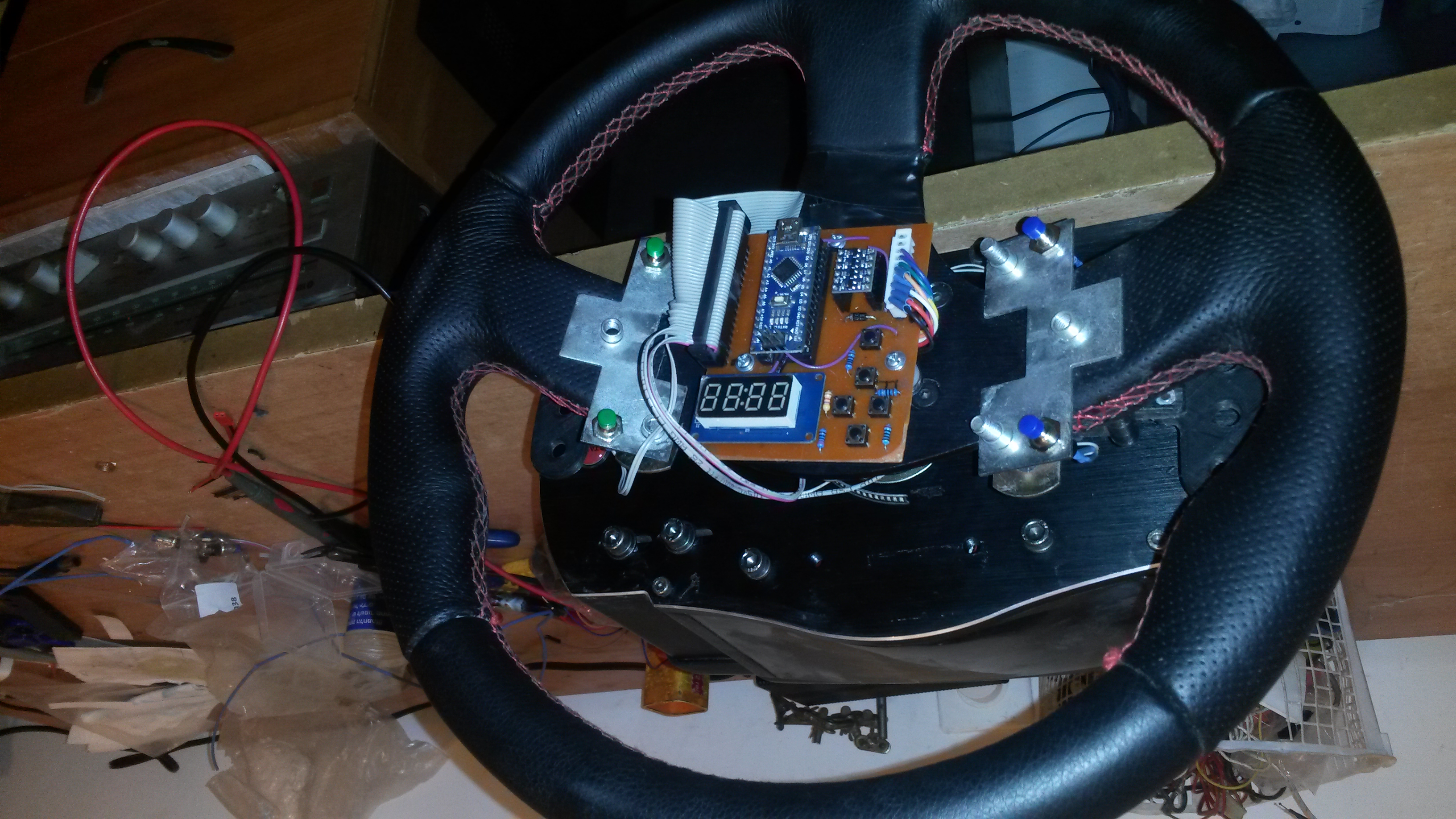
5 | [check out more photos here](https://github.com/lshachar/Arduino_Fanatec_Wheel/tree/master/Steering%20Wheel%20Photos)
6 |
7 | *The buttons delay bug is fixed, buttons code is working great!
8 | *I fixed several large bugs with the SPI communication, which now works flawlessly.
9 | *Updated schematics - Added a 5 buttons Analog input that feeds into a single analog input on the arduino. You can calibrate your wheel center by using the D-pad and alphanumeric display, without plugging the Arduino to your PC!
10 | *Added Diode, and connected D2 and D10 together, both changes are necessary! please revise your board to include these changes if you've built one already!
11 | *Updated board layout - it's possible to either manufacture a single layer board, and solder a few jumper wires for the top layer, or manufacture the complete two-layers board. (I used a CNC machine and milled a single layer board)
12 | ________________
13 |
14 | **This project is donationware, if my work helped you out** [**maybe get me a beer! :)**](https://paypal.me/lshachar?locale.x=en_US)
15 |
16 | Fanatec's wheelbases won't enable any force feedback, unless you have a Fanatec steering wheel attached to it.
17 | With this project, you can use an arduino to communicate with the wheelbase over SPI, which will get the wheelbase working.
18 | You can attach buttons, a D-Pad and an alphanumeric display, for the complete package!
19 |
20 | This simplified (schematics) version is enough to let you enable force feedback on your wheelbase,
21 | [use this easy to understand 'breadboard view' simplified schematics](https://github.com/lshachar/Arduino_Fanatec_Wheel/blob/master/schamtics%20arduino%20nano-level%20shifter-fanatec%20round%20plug.png), or [This simplified schematic](https://github.com/lshachar/Arduino_Fanatec_Wheel/blob/master/schamtics%20arduino%20nano-level%20shifter-Simlified.png).
22 |
23 | The full PCB supports alphanumeric display, D-pad, and lots of external buttons
24 | 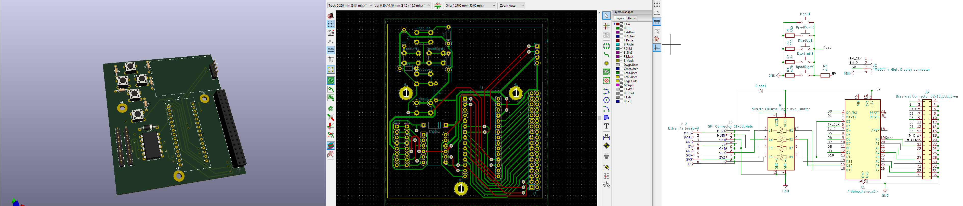 (I currently use 6: 2 paddle shifters and 4 buttons on the rim).
25 |
26 |
27 |
28 | Here's a [how to make a male Fanatec SPI connector](Steering%20wheel%20connector%20-%20howto/Readme.md) (what the steering wheel has)
29 | Also, [Alevale found where to buy the connector](https://github.com/darknao/btClubSportWheel/issues/14#issuecomment-604973137)
30 | [use this](3d%20Models/fanatec%20adapter%20v1.STL) If you need a simple 3d adapter to attach your physical steering wheel to the wheelbase
31 |
32 |
33 |
34 | ### Several options:
35 | - Use a 5V arduino with a logic level shifter. (recommended, this is what I use. [(here are The schematics)](https://github.com/lshachar/Arduino_Fanatec_Wheel/blob/master/schamtics%20arduino%20nano-level%20shifter-fanatec%20round%20plug.png)
36 | - Use a 5V arduino **without** a logic shifter (can be risky to your precious wheelbase)
37 | - Use a 3.3V arduino (I haven't tried it. They run on 8 MHZ instead of 16 MHZ for the 5V arduinos, but I'm pretty sure 8MHZ should be fast enough.)
38 |
39 | Code was tested on arduino Uno and Nano, and works fine. However, they both output 5V and the SPI communication on the wheelbase
40 | is using 3.3V.
41 | It's best to use a level shifter between the two, so there are no chances of damaging the wheelbase (by connecting the 5V arduino
42 | output to a 3.3V wheelbase input)
43 | However, since the wheelbase is the master and the steering wheel is the slave - MISO is the only *input* channel on the wheelbase,
44 | and it is safe to simply use a voltage divider on the MISO line - to go from 5V level to 3.3V. (The arduino should recognize the 3.3V input signals coming from the wheelbase as high, so there's nothing we have to do there).
45 | - **Note:** If you do end up going this route, make sure you wire everything up properly, and that you never set SPI as master on the arduino, or you will subject the wheelbase SPI to 5V. (I did subject the wheelbase SPI to 5V by mistake - and nothing got damaged.)
46 |
47 | I recommend using an arduino nano **and** a logic shifter, as seen in the schematics.
48 | - **Note:** The diode is crucial to keep the 5V coming from the wheelbase, and the 5V coming from the computer USB, seperate. the diode will drop the 5V voltage from the wheelbase to ~4.3V, which is fine for the arduino to run on. When you plug the USB cable, the arduino will run on the 5V coming from the computer, and current cannot flow to the wheelbase because of the diode.
49 | fyi I have connected both power supplies together, and did not have anything go up in smoke. (but this is before I thought about using a diode. DO NOT ATTEMPT THIS YOURSELF.
50 |
51 | [There's a lot of (old) info here](https://github.com/darknao/btClubSportWheel/issues/12)
52 |
53 |
54 | # What to do if you gotta calibrate your wheelbase center?
55 | On some wheelbases, you can do that directly from the [Fanatec wheel properties page](https://github.com/lshachar/Arduino_Fanatec_Wheel/issues/7). unfortunately it doesn't work on my CSW V2.5.
56 | You can use the current code to calibrate the wheelbase's center point. (This is needed after a firmware upgrade for the wheelbase) the arduino will translate the alphanumeric display to letters and send them out to the Serial monitor(!). you will need to type in some commands on the Serial monitor, which will look pretty cypheric to you.
57 | Type these characters on the serial monitor, press [return] after each line:
58 | C (to change bits on the 3rd byte that affects buttons. C=3rd)
59 | 6 (to change (raise) the sixth bit on the 3rd byte, which is the menu button. this will cause the alphanumeric display to turn on and the message '5_1' (equivilent to 'S_1' i.e. 'setting 1') will be printed on the serial monitor.)
60 | 6 (to release the menu button (lower the 6th bit) )
61 | 23 (2 will raise the D-pad button bit, 3 will raise the joystick button bit.)
62 | 23 (to release both buttons, drop both bits)
63 | 6 (press the menu button again to exit the menu)
64 | 6 (release the menu button)
65 | [Watch this If you don't know what I'm talking about](https://www.youtube.com/watch?v=yvhAKxjit8o)
66 | (Hey - it's not an easy procedure, but it works!)
67 | if you made a PCB with a Dpad and alphanumeric display - you can calibrate the center point without connecting to the computer!
68 | Using the Dpad:
69 | Enter the menu by pressing both up+down bubttons on the Dpad,
70 | S_1 will appear on the serial monitor and on the alphanumeric display,
71 | Press both left+right buttons on the Dpad to calibrate wheel center,
72 | Press both up+down on the Dpad to exit menu. Done!
73 |
74 |
75 | This project would never have been possible without the work of Darknao on his [BtClubSportWheel - converting any Fanatec CSW steering wheel to a standalone USB version](https://github.com/darknao/btClubSportWheel) project.
--------------------------------------------------------------------------------
/Schematics & pcb layout/KiCad/Gerber/arduino-fanatec-pcb-B_SilkS.gbo:
--------------------------------------------------------------------------------
1 | G04 #@! TF.GenerationSoftware,KiCad,Pcbnew,(5.1.5)-3*
2 | G04 #@! TF.CreationDate,2022-12-19T02:05:45+02:00*
3 | G04 #@! TF.ProjectId,arduino-fanatec-pcb,61726475-696e-46f2-9d66-616e61746563,rev?*
4 | G04 #@! TF.SameCoordinates,Original*
5 | G04 #@! TF.FileFunction,Legend,Bot*
6 | G04 #@! TF.FilePolarity,Positive*
7 | %FSLAX46Y46*%
8 | G04 Gerber Fmt 4.6, Leading zero omitted, Abs format (unit mm)*
9 | G04 Created by KiCad (PCBNEW (5.1.5)-3) date 2022-12-19 02:05:45*
10 | %MOMM*%
11 | %LPD*%
12 | G04 APERTURE LIST*
13 | %ADD10O,1.702000X1.702000*%
14 | %ADD11R,1.702000X1.702000*%
15 | %ADD12R,1.802000X1.802000*%
16 | %ADD13O,1.802000X1.802000*%
17 | %ADD14C,6.102000*%
18 | %ADD15C,2.102000*%
19 | %ADD16O,1.902000X1.902000*%
20 | %ADD17R,1.902000X1.902000*%
21 | G04 APERTURE END LIST*
22 | %LPC*%
23 | D10*
24 | X101600000Y-105410000D03*
25 | X86360000Y-105410000D03*
26 | X101600000Y-69850000D03*
27 | X86360000Y-102870000D03*
28 | X101600000Y-72390000D03*
29 | X86360000Y-100330000D03*
30 | X101600000Y-74930000D03*
31 | X86360000Y-97790000D03*
32 | X101600000Y-77470000D03*
33 | X86360000Y-95250000D03*
34 | X101600000Y-80010000D03*
35 | X86360000Y-92710000D03*
36 | X101600000Y-82550000D03*
37 | X86360000Y-90170000D03*
38 | X101600000Y-85090000D03*
39 | X86360000Y-87630000D03*
40 | X101600000Y-87630000D03*
41 | X86360000Y-85090000D03*
42 | X101600000Y-90170000D03*
43 | X86360000Y-82550000D03*
44 | X101600000Y-92710000D03*
45 | X86360000Y-80010000D03*
46 | X101600000Y-95250000D03*
47 | X86360000Y-77470000D03*
48 | X101600000Y-97790000D03*
49 | X86360000Y-74930000D03*
50 | X101600000Y-100330000D03*
51 | X86360000Y-72390000D03*
52 | X101600000Y-102870000D03*
53 | D11*
54 | X86360000Y-69850000D03*
55 | D12*
56 | X116840000Y-110490000D03*
57 | D13*
58 | X119380000Y-110490000D03*
59 | X116840000Y-107950000D03*
60 | X119380000Y-107950000D03*
61 | X116840000Y-105410000D03*
62 | X119380000Y-105410000D03*
63 | X116840000Y-102870000D03*
64 | X119380000Y-102870000D03*
65 | X116840000Y-100330000D03*
66 | X119380000Y-100330000D03*
67 | X116840000Y-97790000D03*
68 | X119380000Y-97790000D03*
69 | X116840000Y-95250000D03*
70 | X119380000Y-95250000D03*
71 | X116840000Y-92710000D03*
72 | X119380000Y-92710000D03*
73 | X116840000Y-90170000D03*
74 | X119380000Y-90170000D03*
75 | X116840000Y-87630000D03*
76 | X119380000Y-87630000D03*
77 | X116840000Y-85090000D03*
78 | X119380000Y-85090000D03*
79 | X116840000Y-82550000D03*
80 | X119380000Y-82550000D03*
81 | X116840000Y-80010000D03*
82 | X119380000Y-80010000D03*
83 | X116840000Y-77470000D03*
84 | X119380000Y-77470000D03*
85 | X116840000Y-74930000D03*
86 | X119380000Y-74930000D03*
87 | X116840000Y-72390000D03*
88 | X119380000Y-72390000D03*
89 | X116840000Y-69850000D03*
90 | X119380000Y-69850000D03*
91 | X116840000Y-67310000D03*
92 | X119380000Y-67310000D03*
93 | D11*
94 | X67310000Y-86360000D03*
95 | D10*
96 | X77470000Y-99060000D03*
97 | X67310000Y-88900000D03*
98 | X77470000Y-96520000D03*
99 | X67310000Y-91440000D03*
100 | X77470000Y-93980000D03*
101 | X67310000Y-93980000D03*
102 | X77470000Y-91440000D03*
103 | X67310000Y-96520000D03*
104 | X77470000Y-88900000D03*
105 | X67310000Y-99060000D03*
106 | X77470000Y-86360000D03*
107 | D13*
108 | X55118000Y-100330000D03*
109 | X55118000Y-97790000D03*
110 | X55118000Y-95250000D03*
111 | X55118000Y-92710000D03*
112 | X55118000Y-90170000D03*
113 | X55118000Y-87630000D03*
114 | X55118000Y-85090000D03*
115 | D12*
116 | X55118000Y-82550000D03*
117 | D14*
118 | X84455000Y-111125000D03*
119 | D10*
120 | X56515000Y-55880000D03*
121 | X64135000Y-55880000D03*
122 | X73025000Y-70485000D03*
123 | X73025000Y-62865000D03*
124 | X78740000Y-48895000D03*
125 | X78740000Y-56515000D03*
126 | X58420000Y-45720000D03*
127 | X58420000Y-38100000D03*
128 | X78740000Y-36830000D03*
129 | X78740000Y-44450000D03*
130 | D15*
131 | X70635000Y-71755000D03*
132 | X70635000Y-76255000D03*
133 | X64135000Y-71755000D03*
134 | X64135000Y-76255000D03*
135 | X70635000Y-58420000D03*
136 | X70635000Y-62920000D03*
137 | X64135000Y-58420000D03*
138 | X64135000Y-62920000D03*
139 | X76350000Y-48840000D03*
140 | X76350000Y-53340000D03*
141 | X69850000Y-48840000D03*
142 | X69850000Y-53340000D03*
143 | X64920000Y-48840000D03*
144 | X64920000Y-53340000D03*
145 | X58420000Y-48840000D03*
146 | X58420000Y-53340000D03*
147 | X70635000Y-39370000D03*
148 | X70635000Y-43870000D03*
149 | X64135000Y-39370000D03*
150 | X64135000Y-43870000D03*
151 | D13*
152 | X119380000Y-53340000D03*
153 | X119380000Y-50800000D03*
154 | X119380000Y-48260000D03*
155 | D12*
156 | X119380000Y-45720000D03*
157 | D14*
158 | X109620000Y-67310000D03*
159 | X59290000Y-67310000D03*
160 | D16*
161 | X67310000Y-81915000D03*
162 | D17*
163 | X77470000Y-81915000D03*
164 | D13*
165 | X59690000Y-100330000D03*
166 | X59690000Y-97790000D03*
167 | X59690000Y-95250000D03*
168 | X59690000Y-92710000D03*
169 | X59690000Y-90170000D03*
170 | X59690000Y-87630000D03*
171 | X59690000Y-85090000D03*
172 | D12*
173 | X59690000Y-82550000D03*
174 | M02*
175 |
--------------------------------------------------------------------------------
/Schematics & pcb layout/KiCad/Gerber/arduino-fanatec-pcb-Edge_Cuts.gm1:
--------------------------------------------------------------------------------
1 | G04 #@! TF.GenerationSoftware,KiCad,Pcbnew,(5.1.5)-3*
2 | G04 #@! TF.CreationDate,2022-12-19T02:05:46+02:00*
3 | G04 #@! TF.ProjectId,arduino-fanatec-pcb,61726475-696e-46f2-9d66-616e61746563,rev?*
4 | G04 #@! TF.SameCoordinates,Original*
5 | G04 #@! TF.FileFunction,Profile,NP*
6 | %FSLAX46Y46*%
7 | G04 Gerber Fmt 4.6, Leading zero omitted, Abs format (unit mm)*
8 | G04 Created by KiCad (PCBNEW (5.1.5)-3) date 2022-12-19 02:05:46*
9 | %MOMM*%
10 | %LPD*%
11 | G04 APERTURE LIST*
12 | %ADD10C,0.050000*%
13 | G04 APERTURE END LIST*
14 | D10*
15 | X50800000Y-115570000D02*
16 | X121920000Y-115570000D01*
17 | X50800000Y-35560000D02*
18 | X50800000Y-115570000D01*
19 | X121920000Y-35560000D02*
20 | X50800000Y-35560000D01*
21 | X121920000Y-115570000D02*
22 | X121920000Y-35560000D01*
23 | M02*
24 |
--------------------------------------------------------------------------------
/Schematics & pcb layout/KiCad/Gerber/arduino-fanatec-pcb-NPTH-drl_map.gbr:
--------------------------------------------------------------------------------
1 | %FSLAX45Y45*%
2 | G04 Gerber Fmt 4.5, Leading zero omitted, Abs format (unit mm)*
3 | G04 Created by KiCad (PCBNEW (5.1.5)-3) date 2022-12-19 02:04:39*
4 | %MOMM*%
5 | %LPD*%
6 | G04 APERTURE LIST*
7 | %TA.AperFunction,Profile*%
8 | %ADD10C,0.050000*%
9 | %TD*%
10 | %ADD11C,0.200000*%
11 | %ADD12C,0.300000*%
12 | G04 APERTURE END LIST*
13 | D10*
14 | X5080000Y-11557000D02*
15 | X12192000Y-11557000D01*
16 | X5080000Y-3556000D02*
17 | X5080000Y-11557000D01*
18 | X12192000Y-3556000D02*
19 | X5080000Y-3556000D01*
20 | X12192000Y-11557000D02*
21 | X12192000Y-3556000D01*
22 | D11*
23 | D12*
24 | X5363928Y-12025214D02*
25 | X5363928Y-11725214D01*
26 | X5435357Y-11725214D01*
27 | X5478214Y-11739500D01*
28 | X5506786Y-11768071D01*
29 | X5521071Y-11796643D01*
30 | X5535357Y-11853786D01*
31 | X5535357Y-11896643D01*
32 | X5521071Y-11953786D01*
33 | X5506786Y-11982357D01*
34 | X5478214Y-12010929D01*
35 | X5435357Y-12025214D01*
36 | X5363928Y-12025214D01*
37 | X5663928Y-12025214D02*
38 | X5663928Y-11825214D01*
39 | X5663928Y-11882357D02*
40 | X5678214Y-11853786D01*
41 | X5692500Y-11839500D01*
42 | X5721071Y-11825214D01*
43 | X5749643Y-11825214D01*
44 | X5849643Y-12025214D02*
45 | X5849643Y-11825214D01*
46 | X5849643Y-11725214D02*
47 | X5835357Y-11739500D01*
48 | X5849643Y-11753786D01*
49 | X5863928Y-11739500D01*
50 | X5849643Y-11725214D01*
51 | X5849643Y-11753786D01*
52 | X6035357Y-12025214D02*
53 | X6006786Y-12010929D01*
54 | X5992500Y-11982357D01*
55 | X5992500Y-11725214D01*
56 | X6192500Y-12025214D02*
57 | X6163928Y-12010929D01*
58 | X6149643Y-11982357D01*
59 | X6149643Y-11725214D01*
60 | X6535357Y-12025214D02*
61 | X6535357Y-11725214D01*
62 | X6635357Y-11939500D01*
63 | X6735357Y-11725214D01*
64 | X6735357Y-12025214D01*
65 | X7006786Y-12025214D02*
66 | X7006786Y-11868071D01*
67 | X6992500Y-11839500D01*
68 | X6963928Y-11825214D01*
69 | X6906786Y-11825214D01*
70 | X6878214Y-11839500D01*
71 | X7006786Y-12010929D02*
72 | X6978214Y-12025214D01*
73 | X6906786Y-12025214D01*
74 | X6878214Y-12010929D01*
75 | X6863928Y-11982357D01*
76 | X6863928Y-11953786D01*
77 | X6878214Y-11925214D01*
78 | X6906786Y-11910929D01*
79 | X6978214Y-11910929D01*
80 | X7006786Y-11896643D01*
81 | X7149643Y-11825214D02*
82 | X7149643Y-12125214D01*
83 | X7149643Y-11839500D02*
84 | X7178214Y-11825214D01*
85 | X7235357Y-11825214D01*
86 | X7263928Y-11839500D01*
87 | X7278214Y-11853786D01*
88 | X7292500Y-11882357D01*
89 | X7292500Y-11968071D01*
90 | X7278214Y-11996643D01*
91 | X7263928Y-12010929D01*
92 | X7235357Y-12025214D01*
93 | X7178214Y-12025214D01*
94 | X7149643Y-12010929D01*
95 | X7421071Y-11996643D02*
96 | X7435357Y-12010929D01*
97 | X7421071Y-12025214D01*
98 | X7406786Y-12010929D01*
99 | X7421071Y-11996643D01*
100 | X7421071Y-12025214D01*
101 | X7421071Y-11839500D02*
102 | X7435357Y-11853786D01*
103 | X7421071Y-11868071D01*
104 | X7406786Y-11853786D01*
105 | X7421071Y-11839500D01*
106 | X7421071Y-11868071D01*
107 | M02*
108 |
--------------------------------------------------------------------------------
/Schematics & pcb layout/KiCad/Gerber/arduino-fanatec-pcb-NPTH.drl:
--------------------------------------------------------------------------------
1 | M48
2 | ; DRILL file {KiCad (5.1.5)-3} date 19/12/2022 02:04:33
3 | ; FORMAT={-:-/ absolute / metric / decimal}
4 | ; #@! TF.CreationDate,2022-12-19T02:04:33+02:00
5 | ; #@! TF.GenerationSoftware,Kicad,Pcbnew,(5.1.5)-3
6 | ; #@! TF.FileFunction,NonPlated,1,2,NPTH
7 | FMAT,2
8 | METRIC
9 | %
10 | G90
11 | G05
12 | T0
13 | M30
14 |
--------------------------------------------------------------------------------
/Schematics & pcb layout/KiCad/Gerber/arduino-fanatec-pcb-PTH.drl:
--------------------------------------------------------------------------------
1 | M48
2 | ; DRILL file {KiCad (5.1.5)-3} date 19/12/2022 02:04:33
3 | ; FORMAT={-:-/ absolute / metric / decimal}
4 | ; #@! TF.CreationDate,2022-12-19T02:04:33+02:00
5 | ; #@! TF.GenerationSoftware,Kicad,Pcbnew,(5.1.5)-3
6 | ; #@! TF.FileFunction,Plated,1,2,PTH
7 | FMAT,2
8 | METRIC
9 | T1C0.800
10 | T2C0.900
11 | T3C1.000
12 | T4C1.100
13 | T5C3.000
14 | %
15 | G90
16 | G05
17 | T1
18 | X60.325Y-76.2
19 | X61.75Y-93.98
20 | X63.5Y-88.9
21 | X64.164Y-84.426
22 | X64.477Y-98.287
23 | X65.25Y-93.98
24 | X80.01Y-91.44
25 | X80.01Y-96.52
26 | X83.058Y-102.768
27 | X83.185Y-100.33
28 | X88.9Y-69.85
29 | X88.9Y-72.39
30 | X95.25Y-82.55
31 | X95.33Y-85.09
32 | X98.425Y-97.79
33 | X98.425Y-100.33
34 | X105.41Y-69.84
35 | X105.41Y-74.93
36 | X113.03Y-110.49
37 | X113.03Y-113.03
38 | X113.031Y-107.951
39 | X115.57Y-45.72
40 | X115.57Y-48.26
41 | X78.74Y-48.895
42 | X78.74Y-56.515
43 | X78.74Y-36.83
44 | X78.74Y-44.45
45 | X58.42Y-38.1
46 | X58.42Y-45.72
47 | X86.36Y-69.85
48 | X86.36Y-72.39
49 | X86.36Y-74.93
50 | X86.36Y-77.47
51 | X86.36Y-80.01
52 | X86.36Y-82.55
53 | X86.36Y-85.09
54 | X86.36Y-87.63
55 | X86.36Y-90.17
56 | X86.36Y-92.71
57 | X86.36Y-95.25
58 | X86.36Y-97.79
59 | X86.36Y-100.33
60 | X86.36Y-102.87
61 | X86.36Y-105.41
62 | X101.6Y-69.85
63 | X101.6Y-72.39
64 | X101.6Y-74.93
65 | X101.6Y-77.47
66 | X101.6Y-80.01
67 | X101.6Y-82.55
68 | X101.6Y-85.09
69 | X101.6Y-87.63
70 | X101.6Y-90.17
71 | X101.6Y-92.71
72 | X101.6Y-95.25
73 | X101.6Y-97.79
74 | X101.6Y-100.33
75 | X101.6Y-102.87
76 | X101.6Y-105.41
77 | X73.025Y-62.865
78 | X73.025Y-70.485
79 | X56.515Y-55.88
80 | X64.135Y-55.88
81 | X67.31Y-86.36
82 | X67.31Y-88.9
83 | X67.31Y-91.44
84 | X67.31Y-93.98
85 | X67.31Y-96.52
86 | X67.31Y-99.06
87 | X77.47Y-86.36
88 | X77.47Y-88.9
89 | X77.47Y-91.44
90 | X77.47Y-93.98
91 | X77.47Y-96.52
92 | X77.47Y-99.06
93 | T2
94 | X67.31Y-81.915
95 | X77.47Y-81.915
96 | T3
97 | X119.38Y-45.72
98 | X119.38Y-48.26
99 | X119.38Y-50.8
100 | X119.38Y-53.34
101 | X55.118Y-82.55
102 | X55.118Y-85.09
103 | X55.118Y-87.63
104 | X55.118Y-90.17
105 | X55.118Y-92.71
106 | X55.118Y-95.25
107 | X55.118Y-97.79
108 | X55.118Y-100.33
109 | X59.69Y-82.55
110 | X59.69Y-85.09
111 | X59.69Y-87.63
112 | X59.69Y-90.17
113 | X59.69Y-92.71
114 | X59.69Y-95.25
115 | X59.69Y-97.79
116 | X59.69Y-100.33
117 | X116.84Y-67.31
118 | X116.84Y-69.85
119 | X116.84Y-72.39
120 | X116.84Y-74.93
121 | X116.84Y-77.47
122 | X116.84Y-80.01
123 | X116.84Y-82.55
124 | X116.84Y-85.09
125 | X116.84Y-87.63
126 | X116.84Y-90.17
127 | X116.84Y-92.71
128 | X116.84Y-95.25
129 | X116.84Y-97.79
130 | X116.84Y-100.33
131 | X116.84Y-102.87
132 | X116.84Y-105.41
133 | X116.84Y-107.95
134 | X116.84Y-110.49
135 | X119.38Y-67.31
136 | X119.38Y-69.85
137 | X119.38Y-72.39
138 | X119.38Y-74.93
139 | X119.38Y-77.47
140 | X119.38Y-80.01
141 | X119.38Y-82.55
142 | X119.38Y-85.09
143 | X119.38Y-87.63
144 | X119.38Y-90.17
145 | X119.38Y-92.71
146 | X119.38Y-95.25
147 | X119.38Y-97.79
148 | X119.38Y-100.33
149 | X119.38Y-102.87
150 | X119.38Y-105.41
151 | X119.38Y-107.95
152 | X119.38Y-110.49
153 | T4
154 | X64.135Y-58.42
155 | X64.135Y-62.92
156 | X70.635Y-58.42
157 | X70.635Y-62.92
158 | X64.135Y-39.37
159 | X64.135Y-43.87
160 | X70.635Y-39.37
161 | X70.635Y-43.87
162 | X58.42Y-48.84
163 | X58.42Y-53.34
164 | X64.92Y-48.84
165 | X64.92Y-53.34
166 | X64.135Y-71.755
167 | X64.135Y-76.255
168 | X70.635Y-71.755
169 | X70.635Y-76.255
170 | X69.85Y-48.84
171 | X69.85Y-53.34
172 | X76.35Y-48.84
173 | X76.35Y-53.34
174 | T5
175 | X109.62Y-67.31
176 | X59.29Y-67.31
177 | X84.455Y-111.125
178 | T0
179 | M30
180 |
--------------------------------------------------------------------------------
/Schematics & pcb layout/KiCad/Gerber/arduino_fanatec_wheel_gerber.zip:
--------------------------------------------------------------------------------
https://raw.githubusercontent.com/lshachar/Arduino_Fanatec_Wheel/5fd71bdad0d2714417f2ed00f07f650c1df54569/Schematics & pcb layout/KiCad/Gerber/arduino_fanatec_wheel_gerber.zip
--------------------------------------------------------------------------------
/Schematics & pcb layout/KiCad/arduino-fanatec-pcb-cache.lib:
--------------------------------------------------------------------------------
1 | EESchema-LIBRARY Version 2.4
2 | #encoding utf-8
3 | #
4 | # Connector_Conn_01x04_Female
5 | #
6 | DEF Connector_Conn_01x04_Female J 0 40 Y N 1 F N
7 | F0 "J" 0 200 50 H V C CNN
8 | F1 "Connector_Conn_01x04_Female" 0 -300 50 H V C CNN
9 | F2 "" 0 0 50 H I C CNN
10 | F3 "" 0 0 50 H I C CNN
11 | $FPLIST
12 | Connector*:*_1x??_*
13 | $ENDFPLIST
14 | DRAW
15 | A 0 -200 20 901 -901 1 1 6 N 0 -180 0 -220
16 | A 0 -100 20 901 -901 1 1 6 N 0 -80 0 -120
17 | A 0 0 20 901 -901 1 1 6 N 0 20 0 -20
18 | A 0 100 20 901 -901 1 1 6 N 0 120 0 80
19 | P 2 1 1 6 -50 -200 -20 -200 N
20 | P 2 1 1 6 -50 -100 -20 -100 N
21 | P 2 1 1 6 -50 0 -20 0 N
22 | P 2 1 1 6 -50 100 -20 100 N
23 | X Pin_1 1 -200 100 150 R 50 50 1 1 P
24 | X Pin_2 2 -200 0 150 R 50 50 1 1 P
25 | X Pin_3 3 -200 -100 150 R 50 50 1 1 P
26 | X Pin_4 4 -200 -200 150 R 50 50 1 1 P
27 | ENDDRAW
28 | ENDDEF
29 | #
30 | # Connector_Conn_01x08_Female
31 | #
32 | DEF Connector_Conn_01x08_Female J 0 40 Y N 1 F N
33 | F0 "J" 0 400 50 H V C CNN
34 | F1 "Connector_Conn_01x08_Female" 0 -500 50 H V C CNN
35 | F2 "" 0 0 50 H I C CNN
36 | F3 "" 0 0 50 H I C CNN
37 | $FPLIST
38 | Connector*:*_1x??_*
39 | $ENDFPLIST
40 | DRAW
41 | A 0 -400 20 901 -901 1 1 6 N 0 -380 0 -420
42 | A 0 -300 20 901 -901 1 1 6 N 0 -280 0 -320
43 | A 0 -200 20 901 -901 1 1 6 N 0 -180 0 -220
44 | A 0 -100 20 901 -901 1 1 6 N 0 -80 0 -120
45 | A 0 0 20 901 -901 1 1 6 N 0 20 0 -20
46 | A 0 100 20 901 -901 1 1 6 N 0 120 0 80
47 | A 0 200 20 901 -901 1 1 6 N 0 220 0 180
48 | A 0 300 20 901 -901 1 1 6 N 0 320 0 280
49 | P 2 1 1 6 -50 -400 -20 -400 N
50 | P 2 1 1 6 -50 -300 -20 -300 N
51 | P 2 1 1 6 -50 -200 -20 -200 N
52 | P 2 1 1 6 -50 -100 -20 -100 N
53 | P 2 1 1 6 -50 0 -20 0 N
54 | P 2 1 1 6 -50 100 -20 100 N
55 | P 2 1 1 6 -50 200 -20 200 N
56 | P 2 1 1 6 -50 300 -20 300 N
57 | X Pin_1 1 -200 300 150 R 50 50 1 1 P
58 | X Pin_2 2 -200 200 150 R 50 50 1 1 P
59 | X Pin_3 3 -200 100 150 R 50 50 1 1 P
60 | X Pin_4 4 -200 0 150 R 50 50 1 1 P
61 | X Pin_5 5 -200 -100 150 R 50 50 1 1 P
62 | X Pin_6 6 -200 -200 150 R 50 50 1 1 P
63 | X Pin_7 7 -200 -300 150 R 50 50 1 1 P
64 | X Pin_8 8 -200 -400 150 R 50 50 1 1 P
65 | ENDDRAW
66 | ENDDEF
67 | #
68 | # Connector_Generic_Conn_02x18_Odd_Even
69 | #
70 | DEF Connector_Generic_Conn_02x18_Odd_Even J 0 40 Y N 1 F N
71 | F0 "J" 50 900 50 H V C CNN
72 | F1 "Connector_Generic_Conn_02x18_Odd_Even" 50 -1000 50 H V C CNN
73 | F2 "" 0 0 50 H I C CNN
74 | F3 "" 0 0 50 H I C CNN
75 | $FPLIST
76 | Connector*:*_2x??_*
77 | $ENDFPLIST
78 | DRAW
79 | S -50 -895 0 -905 1 1 6 N
80 | S -50 -795 0 -805 1 1 6 N
81 | S -50 -695 0 -705 1 1 6 N
82 | S -50 -595 0 -605 1 1 6 N
83 | S -50 -495 0 -505 1 1 6 N
84 | S -50 -395 0 -405 1 1 6 N
85 | S -50 -295 0 -305 1 1 6 N
86 | S -50 -195 0 -205 1 1 6 N
87 | S -50 -95 0 -105 1 1 6 N
88 | S -50 5 0 -5 1 1 6 N
89 | S -50 105 0 95 1 1 6 N
90 | S -50 205 0 195 1 1 6 N
91 | S -50 305 0 295 1 1 6 N
92 | S -50 405 0 395 1 1 6 N
93 | S -50 505 0 495 1 1 6 N
94 | S -50 605 0 595 1 1 6 N
95 | S -50 705 0 695 1 1 6 N
96 | S -50 805 0 795 1 1 6 N
97 | S -50 850 150 -950 1 1 10 f
98 | S 150 -895 100 -905 1 1 6 N
99 | S 150 -795 100 -805 1 1 6 N
100 | S 150 -695 100 -705 1 1 6 N
101 | S 150 -595 100 -605 1 1 6 N
102 | S 150 -495 100 -505 1 1 6 N
103 | S 150 -395 100 -405 1 1 6 N
104 | S 150 -295 100 -305 1 1 6 N
105 | S 150 -195 100 -205 1 1 6 N
106 | S 150 -95 100 -105 1 1 6 N
107 | S 150 5 100 -5 1 1 6 N
108 | S 150 105 100 95 1 1 6 N
109 | S 150 205 100 195 1 1 6 N
110 | S 150 305 100 295 1 1 6 N
111 | S 150 405 100 395 1 1 6 N
112 | S 150 505 100 495 1 1 6 N
113 | S 150 605 100 595 1 1 6 N
114 | S 150 705 100 695 1 1 6 N
115 | S 150 805 100 795 1 1 6 N
116 | X Pin_1 1 -200 800 150 R 50 50 1 1 P
117 | X Pin_10 10 300 400 150 L 50 50 1 1 P
118 | X Pin_11 11 -200 300 150 R 50 50 1 1 P
119 | X Pin_12 12 300 300 150 L 50 50 1 1 P
120 | X Pin_13 13 -200 200 150 R 50 50 1 1 P
121 | X Pin_14 14 300 200 150 L 50 50 1 1 P
122 | X Pin_15 15 -200 100 150 R 50 50 1 1 P
123 | X Pin_16 16 300 100 150 L 50 50 1 1 P
124 | X Pin_17 17 -200 0 150 R 50 50 1 1 P
125 | X Pin_18 18 300 0 150 L 50 50 1 1 P
126 | X Pin_19 19 -200 -100 150 R 50 50 1 1 P
127 | X Pin_2 2 300 800 150 L 50 50 1 1 P
128 | X Pin_20 20 300 -100 150 L 50 50 1 1 P
129 | X Pin_21 21 -200 -200 150 R 50 50 1 1 P
130 | X Pin_22 22 300 -200 150 L 50 50 1 1 P
131 | X Pin_23 23 -200 -300 150 R 50 50 1 1 P
132 | X Pin_24 24 300 -300 150 L 50 50 1 1 P
133 | X Pin_25 25 -200 -400 150 R 50 50 1 1 P
134 | X Pin_26 26 300 -400 150 L 50 50 1 1 P
135 | X Pin_27 27 -200 -500 150 R 50 50 1 1 P
136 | X Pin_28 28 300 -500 150 L 50 50 1 1 P
137 | X Pin_29 29 -200 -600 150 R 50 50 1 1 P
138 | X Pin_3 3 -200 700 150 R 50 50 1 1 P
139 | X Pin_30 30 300 -600 150 L 50 50 1 1 P
140 | X Pin_31 31 -200 -700 150 R 50 50 1 1 P
141 | X Pin_32 32 300 -700 150 L 50 50 1 1 P
142 | X Pin_33 33 -200 -800 150 R 50 50 1 1 P
143 | X Pin_34 34 300 -800 150 L 50 50 1 1 P
144 | X Pin_35 35 -200 -900 150 R 50 50 1 1 P
145 | X Pin_36 36 300 -900 150 L 50 50 1 1 P
146 | X Pin_4 4 300 700 150 L 50 50 1 1 P
147 | X Pin_5 5 -200 600 150 R 50 50 1 1 P
148 | X Pin_6 6 300 600 150 L 50 50 1 1 P
149 | X Pin_7 7 -200 500 150 R 50 50 1 1 P
150 | X Pin_8 8 300 500 150 L 50 50 1 1 P
151 | X Pin_9 9 -200 400 150 R 50 50 1 1 P
152 | ENDDRAW
153 | ENDDEF
154 | #
155 | # Device_D_Small
156 | #
157 | DEF Device_D_Small D 0 10 N N 1 F N
158 | F0 "D" -50 80 50 H V L CNN
159 | F1 "Device_D_Small" -150 -80 50 H V L CNN
160 | F2 "" 0 0 50 V I C CNN
161 | F3 "" 0 0 50 V I C CNN
162 | $FPLIST
163 | TO-???*
164 | *_Diode_*
165 | *SingleDiode*
166 | D_*
167 | $ENDFPLIST
168 | DRAW
169 | P 2 0 1 0 -30 -40 -30 40 N
170 | P 2 0 1 0 -30 0 30 0 N
171 | P 4 0 1 0 30 -40 -30 0 30 40 30 -40 N
172 | X K 1 -100 0 70 R 50 50 1 1 P
173 | X A 2 100 0 70 L 50 50 1 1 P
174 | ENDDRAW
175 | ENDDEF
176 | #
177 | # Device_R
178 | #
179 | DEF Device_R R 0 0 N Y 1 F N
180 | F0 "R" 80 0 50 V V C CNN
181 | F1 "Device_R" 0 0 50 V V C CNN
182 | F2 "" -70 0 50 V I C CNN
183 | F3 "" 0 0 50 H I C CNN
184 | $FPLIST
185 | R_*
186 | $ENDFPLIST
187 | DRAW
188 | S -40 -100 40 100 0 1 10 N
189 | X ~ 1 0 150 50 D 50 50 1 1 P
190 | X ~ 2 0 -150 50 U 50 50 1 1 P
191 | ENDDRAW
192 | ENDDEF
193 | #
194 | # Switch_SW_Push
195 | #
196 | DEF Switch_SW_Push SW 0 40 N N 1 F N
197 | F0 "SW" 50 100 50 H V L CNN
198 | F1 "Switch_SW_Push" 0 -60 50 H V C CNN
199 | F2 "" 0 200 50 H I C CNN
200 | F3 "" 0 200 50 H I C CNN
201 | DRAW
202 | C -80 0 20 0 1 0 N
203 | C 80 0 20 0 1 0 N
204 | P 2 0 1 0 0 50 0 120 N
205 | P 2 0 1 0 100 50 -100 50 N
206 | X 1 1 -200 0 100 R 50 50 0 1 P
207 | X 2 2 200 0 100 L 50 50 0 1 P
208 | ENDDRAW
209 | ENDDEF
210 | #
211 | # arduino-fanatec-pcb-rescue_Arduino_Nano_v3.x-MCU_Module
212 | #
213 | DEF arduino-fanatec-pcb-rescue_Arduino_Nano_v3.x-MCU_Module A 0 20 Y Y 1 F N
214 | F0 "A" -200 1025 50 H V R CNN
215 | F1 "arduino-fanatec-pcb-rescue_Arduino_Nano_v3.x-MCU_Module" -200 950 50 H V R CNN
216 | F2 "Module:Arduino_Nano" 150 -950 50 H I L CNN
217 | F3 "" 0 -1000 50 H I C CNN
218 | $FPLIST
219 | Arduino*Nano*
220 | $ENDFPLIST
221 | DRAW
222 | S -400 900 400 -900 0 1 10 f
223 | X D1/TX 1 -500 500 100 R 50 50 1 1 B
224 | X D7 10 -500 -100 100 R 50 50 1 1 B
225 | X D8 11 -500 -200 100 R 50 50 1 1 B
226 | X D9 12 -500 -300 100 R 50 50 1 1 B
227 | X D10 13 -500 -400 100 R 50 50 1 1 B
228 | X D11 14 -500 -500 100 R 50 50 1 1 B
229 | X D12 15 -500 -600 100 R 50 50 1 1 B
230 | X D13 16 -500 -700 100 R 50 50 1 1 B
231 | X 3V3 17 100 1000 100 D 50 50 1 1 w
232 | X AREF 18 500 200 100 L 50 50 1 1 I
233 | X A0 19 500 0 100 L 50 50 1 1 B
234 | X D0/RX 2 -500 600 100 R 50 50 1 1 B
235 | X A1 20 500 -100 100 L 50 50 1 1 B
236 | X A2 21 500 -200 100 L 50 50 1 1 B
237 | X A3 22 500 -300 100 L 50 50 1 1 B
238 | X A4 23 500 -400 100 L 50 50 1 1 B
239 | X A5 24 500 -500 100 L 50 50 1 1 B
240 | X A6 25 500 -600 100 L 50 50 1 1 B
241 | X A7 26 500 -700 100 L 50 50 1 1 B
242 | X +5V 27 200 1000 100 D 50 50 1 1 w
243 | X RESET 28 500 600 100 L 50 50 1 1 I
244 | X GND 29 100 -1000 100 U 50 50 1 1 W
245 | X RESET 3 500 500 100 L 50 50 1 1 I
246 | X VIN 30 -100 1000 100 D 50 50 1 1 W
247 | X GND 4 0 -1000 100 U 50 50 1 1 W
248 | X D2 5 -500 400 100 R 50 50 1 1 B
249 | X D3 6 -500 300 100 R 50 50 1 1 B
250 | X D4 7 -500 200 100 R 50 50 1 1 B
251 | X D5 8 -500 100 100 R 50 50 1 1 B
252 | X D6 9 -500 0 100 R 50 50 1 1 B
253 | ENDDRAW
254 | ENDDEF
255 | #
256 | # arduino-fanatec-pcb-rescue_Simple_Chinese_Logic_level_shifter-Logic_LevelTranslator
257 | #
258 | DEF arduino-fanatec-pcb-rescue_Simple_Chinese_Logic_level_shifter-Logic_LevelTranslator U 0 20 Y Y 1 F N
259 | F0 "U" -250 650 50 H V C CNN
260 | F1 "arduino-fanatec-pcb-rescue_Simple_Chinese_Logic_level_shifter-Logic_LevelTranslator" 150 650 50 H V L CNN
261 | F2 "Package_DIP:DIP-12_W10.16mm" 0 -750 50 H I C CNN
262 | F3 "" 110 95 50 H I C CNN
263 | $FPLIST
264 | Texas*R*PUQFN*N12*
265 | $ENDFPLIST
266 | DRAW
267 | S -300 600 300 -600 0 1 10 f
268 | P 3 0 1 0 -90 -305 -90 -265 -20 -265 N
269 | P 3 0 1 0 -90 -105 -90 -65 -20 -65 N
270 | P 3 0 1 0 -90 95 -90 135 -20 135 N
271 | P 3 0 1 0 -90 295 -90 335 -20 335 N
272 | P 3 0 1 0 120 -305 120 -345 50 -345 N
273 | P 3 0 1 0 120 -105 120 -145 50 -145 N
274 | P 3 0 1 0 120 95 120 55 50 55 N
275 | P 3 0 1 0 120 295 120 255 50 255 N
276 | P 4 0 1 0 -20 -345 -90 -345 -90 -305 -160 -305 N
277 | P 4 0 1 0 -20 -345 50 -305 50 -385 -20 -345 N
278 | P 4 0 1 0 -20 -145 -90 -145 -90 -105 -160 -105 N
279 | P 4 0 1 0 -20 -145 50 -105 50 -185 -20 -145 N
280 | P 4 0 1 0 -20 55 -90 55 -90 95 -160 95 N
281 | P 4 0 1 0 -20 55 50 95 50 15 -20 55 N
282 | P 4 0 1 0 -20 255 -90 255 -90 295 -170 295 N
283 | P 4 0 1 0 -20 255 50 295 50 215 -20 255 N
284 | P 4 0 1 0 50 -265 -20 -305 -20 -225 50 -265 N
285 | P 4 0 1 0 50 -265 120 -265 120 -305 170 -305 N
286 | P 4 0 1 0 50 -65 -20 -105 -20 -25 50 -65 N
287 | P 4 0 1 0 50 -65 120 -65 120 -105 170 -105 N
288 | P 4 0 1 0 50 135 -20 95 -20 175 50 135 N
289 | P 4 0 1 0 50 135 120 135 120 95 170 95 N
290 | P 4 0 1 0 50 335 -20 295 -20 375 50 335 N
291 | P 4 0 1 0 50 335 120 335 120 295 170 295 N
292 | X VCCL 1 -100 700 100 D 50 50 1 1 W
293 | X H1 10 400 300 100 L 50 50 1 1 T
294 | X VCCH 11 100 700 100 D 50 50 1 1 W
295 | X GND-L 12 -100 -700 100 U 50 50 1 1 W
296 | X L1 2 -400 300 100 R 50 50 1 1 T
297 | X L2 3 -400 100 100 R 50 50 1 1 T
298 | X L3 4 -400 -100 100 R 50 50 1 1 T
299 | X L4 5 -400 -300 100 R 50 50 1 1 T
300 | X GND-H 6 100 -700 100 U 50 50 1 1 W
301 | X H4 7 400 -300 100 L 50 50 1 1 T
302 | X H3 8 400 -100 100 L 50 50 1 1 T
303 | X H2 9 400 100 100 L 50 50 1 1 T
304 | ENDDRAW
305 | ENDDEF
306 | #
307 | # power_GND
308 | #
309 | DEF power_GND #PWR 0 0 Y Y 1 F P
310 | F0 "#PWR" 0 -250 50 H I C CNN
311 | F1 "power_GND" 0 -150 50 H V C CNN
312 | F2 "" 0 0 50 H I C CNN
313 | F3 "" 0 0 50 H I C CNN
314 | DRAW
315 | P 6 0 1 0 0 0 0 -50 50 -50 0 -100 -50 -50 0 -50 N
316 | X GND 1 0 0 0 D 50 50 1 1 W N
317 | ENDDRAW
318 | ENDDEF
319 | #
320 | #End Library
321 |
--------------------------------------------------------------------------------
/Schematics & pcb layout/KiCad/arduino-fanatec-pcb-rescue.dcm:
--------------------------------------------------------------------------------
1 | EESchema-DOCLIB Version 2.0
2 | #
3 | #End Doc Library
4 |
--------------------------------------------------------------------------------
/Schematics & pcb layout/KiCad/arduino-fanatec-pcb-rescue.lib:
--------------------------------------------------------------------------------
1 | EESchema-LIBRARY Version 2.4
2 | #encoding utf-8
3 | #
4 | # Arduino_Nano_v3.x-MCU_Module
5 | #
6 | DEF Arduino_Nano_v3.x-MCU_Module A 0 20 Y Y 1 F N
7 | F0 "A" -200 1025 50 H V R CNN
8 | F1 "Arduino_Nano_v3.x-MCU_Module" -200 950 50 H V R CNN
9 | F2 "Module:Arduino_Nano" 150 -950 50 H I L CNN
10 | F3 "" 0 -1000 50 H I C CNN
11 | $FPLIST
12 | Arduino*Nano*
13 | $ENDFPLIST
14 | DRAW
15 | S -400 900 400 -900 0 1 10 f
16 | X D1/TX 1 -500 500 100 R 50 50 1 1 B
17 | X D7 10 -500 -100 100 R 50 50 1 1 B
18 | X D8 11 -500 -200 100 R 50 50 1 1 B
19 | X D9 12 -500 -300 100 R 50 50 1 1 B
20 | X D10 13 -500 -400 100 R 50 50 1 1 B
21 | X D11 14 -500 -500 100 R 50 50 1 1 B
22 | X D12 15 -500 -600 100 R 50 50 1 1 B
23 | X D13 16 -500 -700 100 R 50 50 1 1 B
24 | X 3V3 17 100 1000 100 D 50 50 1 1 w
25 | X AREF 18 500 200 100 L 50 50 1 1 I
26 | X A0 19 500 0 100 L 50 50 1 1 B
27 | X D0/RX 2 -500 600 100 R 50 50 1 1 B
28 | X A1 20 500 -100 100 L 50 50 1 1 B
29 | X A2 21 500 -200 100 L 50 50 1 1 B
30 | X A3 22 500 -300 100 L 50 50 1 1 B
31 | X A4 23 500 -400 100 L 50 50 1 1 B
32 | X A5 24 500 -500 100 L 50 50 1 1 B
33 | X A6 25 500 -600 100 L 50 50 1 1 B
34 | X A7 26 500 -700 100 L 50 50 1 1 B
35 | X +5V 27 200 1000 100 D 50 50 1 1 w
36 | X RESET 28 500 600 100 L 50 50 1 1 I
37 | X GND 29 100 -1000 100 U 50 50 1 1 W
38 | X RESET 3 500 500 100 L 50 50 1 1 I
39 | X VIN 30 -100 1000 100 D 50 50 1 1 W
40 | X GND 4 0 -1000 100 U 50 50 1 1 W
41 | X D2 5 -500 400 100 R 50 50 1 1 B
42 | X D3 6 -500 300 100 R 50 50 1 1 B
43 | X D4 7 -500 200 100 R 50 50 1 1 B
44 | X D5 8 -500 100 100 R 50 50 1 1 B
45 | X D6 9 -500 0 100 R 50 50 1 1 B
46 | ENDDRAW
47 | ENDDEF
48 | #
49 | # Simple_Chinese_Logic_level_shifter-Logic_LevelTranslator
50 | #
51 | DEF Simple_Chinese_Logic_level_shifter-Logic_LevelTranslator U 0 20 Y Y 1 F N
52 | F0 "U" -250 650 50 H V C CNN
53 | F1 "Simple_Chinese_Logic_level_shifter-Logic_LevelTranslator" 150 650 50 H V L CNN
54 | F2 "Package_DIP:DIP-12_W10.16mm" 0 -750 50 H I C CNN
55 | F3 "" 110 95 50 H I C CNN
56 | $FPLIST
57 | Texas*R*PUQFN*N12*
58 | $ENDFPLIST
59 | DRAW
60 | S -300 600 300 -600 0 1 10 f
61 | P 3 0 1 0 -90 -305 -90 -265 -20 -265 N
62 | P 3 0 1 0 -90 -105 -90 -65 -20 -65 N
63 | P 3 0 1 0 -90 95 -90 135 -20 135 N
64 | P 3 0 1 0 -90 295 -90 335 -20 335 N
65 | P 3 0 1 0 120 -305 120 -345 50 -345 N
66 | P 3 0 1 0 120 -105 120 -145 50 -145 N
67 | P 3 0 1 0 120 95 120 55 50 55 N
68 | P 3 0 1 0 120 295 120 255 50 255 N
69 | P 4 0 1 0 -20 -345 -90 -345 -90 -305 -160 -305 N
70 | P 4 0 1 0 -20 -345 50 -305 50 -385 -20 -345 N
71 | P 4 0 1 0 -20 -145 -90 -145 -90 -105 -160 -105 N
72 | P 4 0 1 0 -20 -145 50 -105 50 -185 -20 -145 N
73 | P 4 0 1 0 -20 55 -90 55 -90 95 -160 95 N
74 | P 4 0 1 0 -20 55 50 95 50 15 -20 55 N
75 | P 4 0 1 0 -20 255 -90 255 -90 295 -170 295 N
76 | P 4 0 1 0 -20 255 50 295 50 215 -20 255 N
77 | P 4 0 1 0 50 -265 -20 -305 -20 -225 50 -265 N
78 | P 4 0 1 0 50 -265 120 -265 120 -305 170 -305 N
79 | P 4 0 1 0 50 -65 -20 -105 -20 -25 50 -65 N
80 | P 4 0 1 0 50 -65 120 -65 120 -105 170 -105 N
81 | P 4 0 1 0 50 135 -20 95 -20 175 50 135 N
82 | P 4 0 1 0 50 135 120 135 120 95 170 95 N
83 | P 4 0 1 0 50 335 -20 295 -20 375 50 335 N
84 | P 4 0 1 0 50 335 120 335 120 295 170 295 N
85 | X VCCL 1 -100 700 100 D 50 50 1 1 W
86 | X H1 10 400 300 100 L 50 50 1 1 T
87 | X VCCH 11 100 700 100 D 50 50 1 1 W
88 | X GND-L 12 -100 -700 100 U 50 50 1 1 W
89 | X L1 2 -400 300 100 R 50 50 1 1 T
90 | X L2 3 -400 100 100 R 50 50 1 1 T
91 | X L3 4 -400 -100 100 R 50 50 1 1 T
92 | X L4 5 -400 -300 100 R 50 50 1 1 T
93 | X GND-H 6 100 -700 100 U 50 50 1 1 W
94 | X H4 7 400 -300 100 L 50 50 1 1 T
95 | X H3 8 400 -100 100 L 50 50 1 1 T
96 | X H2 9 400 100 100 L 50 50 1 1 T
97 | ENDDRAW
98 | ENDDEF
99 | #
100 | #End Library
101 |
--------------------------------------------------------------------------------
/Schematics & pcb layout/KiCad/arduino-fanatec-pcb-simplified-cache.lib:
--------------------------------------------------------------------------------
1 | EESchema-LIBRARY Version 2.4
2 | #encoding utf-8
3 | #
4 | # Connector_Conn_01x08_Female
5 | #
6 | DEF Connector_Conn_01x08_Female J 0 40 Y N 1 F N
7 | F0 "J" 0 400 50 H V C CNN
8 | F1 "Connector_Conn_01x08_Female" 0 -500 50 H V C CNN
9 | F2 "" 0 0 50 H I C CNN
10 | F3 "" 0 0 50 H I C CNN
11 | $FPLIST
12 | Connector*:*_1x??_*
13 | $ENDFPLIST
14 | DRAW
15 | A 0 -400 20 901 -901 1 1 6 N 0 -380 0 -420
16 | A 0 -300 20 901 -901 1 1 6 N 0 -280 0 -320
17 | A 0 -200 20 901 -901 1 1 6 N 0 -180 0 -220
18 | A 0 -100 20 901 -901 1 1 6 N 0 -80 0 -120
19 | A 0 0 20 901 -901 1 1 6 N 0 20 0 -20
20 | A 0 100 20 901 -901 1 1 6 N 0 120 0 80
21 | A 0 200 20 901 -901 1 1 6 N 0 220 0 180
22 | A 0 300 20 901 -901 1 1 6 N 0 320 0 280
23 | P 2 1 1 6 -50 -400 -20 -400 N
24 | P 2 1 1 6 -50 -300 -20 -300 N
25 | P 2 1 1 6 -50 -200 -20 -200 N
26 | P 2 1 1 6 -50 -100 -20 -100 N
27 | P 2 1 1 6 -50 0 -20 0 N
28 | P 2 1 1 6 -50 100 -20 100 N
29 | P 2 1 1 6 -50 200 -20 200 N
30 | P 2 1 1 6 -50 300 -20 300 N
31 | X Pin_1 1 -200 300 150 R 50 50 1 1 P
32 | X Pin_2 2 -200 200 150 R 50 50 1 1 P
33 | X Pin_3 3 -200 100 150 R 50 50 1 1 P
34 | X Pin_4 4 -200 0 150 R 50 50 1 1 P
35 | X Pin_5 5 -200 -100 150 R 50 50 1 1 P
36 | X Pin_6 6 -200 -200 150 R 50 50 1 1 P
37 | X Pin_7 7 -200 -300 150 R 50 50 1 1 P
38 | X Pin_8 8 -200 -400 150 R 50 50 1 1 P
39 | ENDDRAW
40 | ENDDEF
41 | #
42 | # Device_D_Small
43 | #
44 | DEF Device_D_Small D 0 10 N N 1 F N
45 | F0 "D" -50 80 50 H V L CNN
46 | F1 "Device_D_Small" -150 -80 50 H V L CNN
47 | F2 "" 0 0 50 V I C CNN
48 | F3 "" 0 0 50 V I C CNN
49 | $FPLIST
50 | TO-???*
51 | *_Diode_*
52 | *SingleDiode*
53 | D_*
54 | $ENDFPLIST
55 | DRAW
56 | P 2 0 1 0 -30 -40 -30 40 N
57 | P 2 0 1 0 -30 0 30 0 N
58 | P 4 0 1 0 30 -40 -30 0 30 40 30 -40 N
59 | X K 1 -100 0 70 R 50 50 1 1 P
60 | X A 2 100 0 70 L 50 50 1 1 P
61 | ENDDRAW
62 | ENDDEF
63 | #
64 | # arduino-fanatec-pcb-rescue_Arduino_Nano_v3.x-MCU_Module
65 | #
66 | DEF arduino-fanatec-pcb-rescue_Arduino_Nano_v3.x-MCU_Module A 0 20 Y Y 1 F N
67 | F0 "A" -200 1025 50 H V R CNN
68 | F1 "arduino-fanatec-pcb-rescue_Arduino_Nano_v3.x-MCU_Module" -200 950 50 H V R CNN
69 | F2 "Module:Arduino_Nano" 150 -950 50 H I L CNN
70 | F3 "" 0 -1000 50 H I C CNN
71 | $FPLIST
72 | Arduino*Nano*
73 | $ENDFPLIST
74 | DRAW
75 | S -400 900 400 -900 0 1 10 f
76 | X D1/TX 1 -500 500 100 R 50 50 1 1 B
77 | X D7 10 -500 -100 100 R 50 50 1 1 B
78 | X D8 11 -500 -200 100 R 50 50 1 1 B
79 | X D9 12 -500 -300 100 R 50 50 1 1 B
80 | X D10 13 -500 -400 100 R 50 50 1 1 B
81 | X D11 14 -500 -500 100 R 50 50 1 1 B
82 | X D12 15 -500 -600 100 R 50 50 1 1 B
83 | X D13 16 -500 -700 100 R 50 50 1 1 B
84 | X 3V3 17 100 1000 100 D 50 50 1 1 w
85 | X AREF 18 500 200 100 L 50 50 1 1 I
86 | X A0 19 500 0 100 L 50 50 1 1 B
87 | X D0/RX 2 -500 600 100 R 50 50 1 1 B
88 | X A1 20 500 -100 100 L 50 50 1 1 B
89 | X A2 21 500 -200 100 L 50 50 1 1 B
90 | X A3 22 500 -300 100 L 50 50 1 1 B
91 | X A4 23 500 -400 100 L 50 50 1 1 B
92 | X A5 24 500 -500 100 L 50 50 1 1 B
93 | X A6 25 500 -600 100 L 50 50 1 1 B
94 | X A7 26 500 -700 100 L 50 50 1 1 B
95 | X +5V 27 200 1000 100 D 50 50 1 1 w
96 | X RESET 28 500 600 100 L 50 50 1 1 I
97 | X GND 29 100 -1000 100 U 50 50 1 1 W
98 | X RESET 3 500 500 100 L 50 50 1 1 I
99 | X VIN 30 -100 1000 100 D 50 50 1 1 W
100 | X GND 4 0 -1000 100 U 50 50 1 1 W
101 | X D2 5 -500 400 100 R 50 50 1 1 B
102 | X D3 6 -500 300 100 R 50 50 1 1 B
103 | X D4 7 -500 200 100 R 50 50 1 1 B
104 | X D5 8 -500 100 100 R 50 50 1 1 B
105 | X D6 9 -500 0 100 R 50 50 1 1 B
106 | ENDDRAW
107 | ENDDEF
108 | #
109 | # arduino-fanatec-pcb-rescue_Simple_Chinese_Logic_level_shifter-Logic_LevelTranslator
110 | #
111 | DEF arduino-fanatec-pcb-rescue_Simple_Chinese_Logic_level_shifter-Logic_LevelTranslator U 0 20 Y Y 1 F N
112 | F0 "U" -250 650 50 H V C CNN
113 | F1 "arduino-fanatec-pcb-rescue_Simple_Chinese_Logic_level_shifter-Logic_LevelTranslator" 150 650 50 H V L CNN
114 | F2 "Package_DIP:DIP-12_W10.16mm" 0 -750 50 H I C CNN
115 | F3 "" 110 95 50 H I C CNN
116 | $FPLIST
117 | Texas*R*PUQFN*N12*
118 | $ENDFPLIST
119 | DRAW
120 | S -300 600 300 -600 0 1 10 f
121 | P 3 0 1 0 -90 -305 -90 -265 -20 -265 N
122 | P 3 0 1 0 -90 -105 -90 -65 -20 -65 N
123 | P 3 0 1 0 -90 95 -90 135 -20 135 N
124 | P 3 0 1 0 -90 295 -90 335 -20 335 N
125 | P 3 0 1 0 120 -305 120 -345 50 -345 N
126 | P 3 0 1 0 120 -105 120 -145 50 -145 N
127 | P 3 0 1 0 120 95 120 55 50 55 N
128 | P 3 0 1 0 120 295 120 255 50 255 N
129 | P 4 0 1 0 -20 -345 -90 -345 -90 -305 -160 -305 N
130 | P 4 0 1 0 -20 -345 50 -305 50 -385 -20 -345 N
131 | P 4 0 1 0 -20 -145 -90 -145 -90 -105 -160 -105 N
132 | P 4 0 1 0 -20 -145 50 -105 50 -185 -20 -145 N
133 | P 4 0 1 0 -20 55 -90 55 -90 95 -160 95 N
134 | P 4 0 1 0 -20 55 50 95 50 15 -20 55 N
135 | P 4 0 1 0 -20 255 -90 255 -90 295 -170 295 N
136 | P 4 0 1 0 -20 255 50 295 50 215 -20 255 N
137 | P 4 0 1 0 50 -265 -20 -305 -20 -225 50 -265 N
138 | P 4 0 1 0 50 -265 120 -265 120 -305 170 -305 N
139 | P 4 0 1 0 50 -65 -20 -105 -20 -25 50 -65 N
140 | P 4 0 1 0 50 -65 120 -65 120 -105 170 -105 N
141 | P 4 0 1 0 50 135 -20 95 -20 175 50 135 N
142 | P 4 0 1 0 50 135 120 135 120 95 170 95 N
143 | P 4 0 1 0 50 335 -20 295 -20 375 50 335 N
144 | P 4 0 1 0 50 335 120 335 120 295 170 295 N
145 | X VCCL 1 -100 700 100 D 50 50 1 1 W
146 | X H1 10 400 300 100 L 50 50 1 1 T
147 | X VCCH 11 100 700 100 D 50 50 1 1 W
148 | X GND-L 12 -100 -700 100 U 50 50 1 1 W
149 | X L1 2 -400 300 100 R 50 50 1 1 T
150 | X L2 3 -400 100 100 R 50 50 1 1 T
151 | X L3 4 -400 -100 100 R 50 50 1 1 T
152 | X L4 5 -400 -300 100 R 50 50 1 1 T
153 | X GND-H 6 100 -700 100 U 50 50 1 1 W
154 | X H4 7 400 -300 100 L 50 50 1 1 T
155 | X H3 8 400 -100 100 L 50 50 1 1 T
156 | X H2 9 400 100 100 L 50 50 1 1 T
157 | ENDDRAW
158 | ENDDEF
159 | #
160 | # power_GND
161 | #
162 | DEF power_GND #PWR 0 0 Y Y 1 F P
163 | F0 "#PWR" 0 -250 50 H I C CNN
164 | F1 "power_GND" 0 -150 50 H V C CNN
165 | F2 "" 0 0 50 H I C CNN
166 | F3 "" 0 0 50 H I C CNN
167 | DRAW
168 | P 6 0 1 0 0 0 0 -50 50 -50 0 -100 -50 -50 0 -50 N
169 | X GND 1 0 0 0 D 50 50 1 1 W N
170 | ENDDRAW
171 | ENDDEF
172 | #
173 | #End Library
174 |
--------------------------------------------------------------------------------
/Schematics & pcb layout/KiCad/arduino-fanatec-pcb-simplified.pro:
--------------------------------------------------------------------------------
1 | update=22/05/2015 07:44:53
2 | version=1
3 | last_client=kicad
4 | [general]
5 | version=1
6 | RootSch=
7 | BoardNm=
8 | [pcbnew]
9 | version=1
10 | LastNetListRead=
11 | UseCmpFile=1
12 | PadDrill=0.600000000000
13 | PadDrillOvalY=0.600000000000
14 | PadSizeH=1.500000000000
15 | PadSizeV=1.500000000000
16 | PcbTextSizeV=1.500000000000
17 | PcbTextSizeH=1.500000000000
18 | PcbTextThickness=0.300000000000
19 | ModuleTextSizeV=1.000000000000
20 | ModuleTextSizeH=1.000000000000
21 | ModuleTextSizeThickness=0.150000000000
22 | SolderMaskClearance=0.000000000000
23 | SolderMaskMinWidth=0.000000000000
24 | DrawSegmentWidth=0.200000000000
25 | BoardOutlineThickness=0.100000000000
26 | ModuleOutlineThickness=0.150000000000
27 | [cvpcb]
28 | version=1
29 | NetIExt=net
30 | [eeschema]
31 | version=1
32 | LibDir=
33 | [eeschema/libraries]
34 |
--------------------------------------------------------------------------------
/Schematics & pcb layout/KiCad/arduino-fanatec-pcb-simplified.sch:
--------------------------------------------------------------------------------
1 | EESchema Schematic File Version 4
2 | EELAYER 30 0
3 | EELAYER END
4 | $Descr A4 11693 8268
5 | encoding utf-8
6 | Sheet 1 1
7 | Title ""
8 | Date ""
9 | Rev ""
10 | Comp ""
11 | Comment1 ""
12 | Comment2 ""
13 | Comment3 ""
14 | Comment4 ""
15 | $EndDescr
16 | $Comp
17 | L arduino-fanatec-pcb-rescue:Simple_Chinese_Logic_level_shifter-Logic_LevelTranslator U1
18 | U 1 1 5E047133
19 | P 4000 4650
20 | F 0 "U1" H 4000 5531 50 0000 C CNN
21 | F 1 "Simple_Chinese_Logic_level_shifter" H 4000 5440 50 0000 C CNN
22 | F 2 "Package_DIP:DIP-12_W10.16mm" H 4000 3900 50 0001 C CNN
23 | F 3 "https://www.aliexpress.com/item/1972789887.html?spm=a2g0o.productlist.0.0.bbfa6f2fPhqdNn&algo_pvid=2205d59a-1fc0-49a4-90b1-846e095ca41e&algo_expid=2205d59a-1fc0-49a4-90b1-846e095ca41e-0&btsid=993594d5-036f-4640-9256-54d97fdaf998&ws_ab_test=searchweb0_0,searchweb201602_1,searchweb201603_53" H 4110 4745 50 0001 C CNN
24 | 1 4000 4650
25 | 1 0 0 -1
26 | $EndComp
27 | $Comp
28 | L power:GND #PWR0101
29 | U 1 1 5E0466D1
30 | P 4100 5550
31 | F 0 "#PWR0101" H 4100 5300 50 0001 C CNN
32 | F 1 "GND" H 4105 5377 50 0000 C CNN
33 | F 2 "" H 4100 5550 50 0001 C CNN
34 | F 3 "" H 4100 5550 50 0001 C CNN
35 | 1 4100 5550
36 | 1 0 0 -1
37 | $EndComp
38 | Wire Wire Line
39 | 4100 5350 4100 5550
40 | Wire Wire Line
41 | 3600 4550 3300 4550
42 | Wire Wire Line
43 | 3300 4550 3300 4350
44 | Wire Wire Line
45 | 3300 4350 2950 4350
46 | Wire Wire Line
47 | 3600 4750 3200 4750
48 | Wire Wire Line
49 | 3200 4750 3200 4450
50 | Wire Wire Line
51 | 3200 4450 2950 4450
52 | Wire Wire Line
53 | 3900 5350 3100 5350
54 | Wire Wire Line
55 | 3100 5350 3100 4750
56 | Wire Wire Line
57 | 3100 4550 2950 4550
58 | Wire Wire Line
59 | 2950 4750 3100 4750
60 | Connection ~ 3100 4750
61 | Wire Wire Line
62 | 3100 4750 3100 4550
63 | Wire Wire Line
64 | 3600 4350 3400 4350
65 | Wire Wire Line
66 | 3400 4350 3400 4850
67 | Wire Wire Line
68 | 3400 4850 2950 4850
69 | Wire Wire Line
70 | 3500 4950 3500 3950
71 | Wire Wire Line
72 | 3500 3950 3900 3950
73 | Wire Wire Line
74 | 3600 4950 3600 5050
75 | Wire Wire Line
76 | 3600 5050 2950 5050
77 | $Comp
78 | L Device:D_Small Diode1
79 | U 1 1 5E0EED80
80 | P 3550 3450
81 | F 0 "Diode1" H 3550 3563 50 0000 C CNN
82 | F 1 "." H 3550 3564 50 0001 C CNN
83 | F 2 "Diode_THT:D_5W_P10.16mm_Horizontal" V 3550 3450 50 0001 C CNN
84 | F 3 "~" V 3550 3450 50 0001 C CNN
85 | 1 3550 3450
86 | -1 0 0 -1
87 | $EndComp
88 | Wire Wire Line
89 | 3000 3450 3450 3450
90 | $Comp
91 | L Connector:Conn_01x08_Female J1
92 | U 1 1 5E07D8D7
93 | P 2750 4650
94 | F 0 "J1" H 2642 5135 50 0000 C CNN
95 | F 1 "SPI Connector 01x08_Male" H 2642 5044 50 0000 C CNN
96 | F 2 "Connector_PinHeader_2.54mm:PinHeader_1x08_P2.54mm_Vertical" H 2750 4650 50 0001 C CNN
97 | F 3 "~" H 2750 4650 50 0001 C CNN
98 | 1 2750 4650
99 | -1 0 0 -1
100 | $EndComp
101 | Wire Wire Line
102 | 2950 4950 3500 4950
103 | Wire Wire Line
104 | 2950 4650 3000 4650
105 | Wire Wire Line
106 | 3000 4650 3000 3450
107 | Text Notes 2600 4800 0 50 ~ 0
108 | GND
109 | Text Notes 2600 4600 0 50 ~ 0
110 | GND
111 | Text Notes 2650 4700 0 50 ~ 0
112 | 5V
113 | Text Notes 2650 5100 0 50 ~ 0
114 | CS
115 | Text Notes 2600 5000 0 50 ~ 0
116 | 3V3
117 | Text Notes 2600 4900 0 50 ~ 0
118 | SCK
119 | Text Notes 2550 4500 0 50 ~ 0
120 | MOSI
121 | Text Notes 2550 4400 0 50 ~ 0
122 | MISO
123 | Text Label 5050 4650 0 50 ~ 0
124 | D7
125 | Wire Wire Line
126 | 5350 4850 5050 4850
127 | Wire Wire Line
128 | 5350 4750 5050 4750
129 | Wire Wire Line
130 | 5350 4650 5050 4650
131 | Wire Wire Line
132 | 5350 4550 5050 4550
133 | Wire Wire Line
134 | 5350 4450 5050 4450
135 | Wire Wire Line
136 | 5350 4350 5050 4350
137 | Text Label 5050 4350 0 50 ~ 0
138 | TM_D
139 | Text Label 5050 4250 0 50 ~ 0
140 | TM_CLK
141 | Wire Wire Line
142 | 5050 3950 5350 3950
143 | Wire Wire Line
144 | 5050 4050 5350 4050
145 | Wire Wire Line
146 | 5050 4250 5350 4250
147 | Wire Wire Line
148 | 6050 3450 6150 3450
149 | Wire Wire Line
150 | 6050 3550 6050 3450
151 | Text Label 6150 3450 0 50 ~ 0
152 | 5V
153 | Text Label 5050 4950 0 50 ~ 0
154 | D10
155 | Text Label 5050 4850 0 50 ~ 0
156 | D9
157 | Text Label 5050 4450 0 50 ~ 0
158 | D5
159 | Text Label 5050 4550 0 50 ~ 0
160 | D6
161 | Text Label 5050 4750 0 50 ~ 0
162 | D8
163 | Text Label 5050 4050 0 50 ~ 0
164 | D1
165 | Text Label 5050 3950 0 50 ~ 0
166 | D0
167 | Wire Wire Line
168 | 6350 5550 6350 5650
169 | Wire Wire Line
170 | 5950 5550 6350 5550
171 | $Comp
172 | L power:GND #PWR0102
173 | U 1 1 5E047AF8
174 | P 6350 5650
175 | F 0 "#PWR0102" H 6350 5400 50 0001 C CNN
176 | F 1 "GND" H 6355 5477 50 0000 C CNN
177 | F 2 "" H 6350 5650 50 0001 C CNN
178 | F 3 "" H 6350 5650 50 0001 C CNN
179 | 1 6350 5650
180 | 1 0 0 -1
181 | $EndComp
182 | $Comp
183 | L arduino-fanatec-pcb-rescue:Arduino_Nano_v3.x-MCU_Module A1
184 | U 1 1 5E03D530
185 | P 5850 4550
186 | F 0 "A1" H 5850 3461 50 0000 C CNN
187 | F 1 "Arduino_Nano_v3.x" H 5850 3370 50 0000 C CNN
188 | F 2 "Module:Arduino_Nano" H 6000 3600 50 0001 L CNN
189 | F 3 "http://www.mouser.com/pdfdocs/Gravitech_Arduino_Nano3_0.pdf" H 5850 3550 50 0001 C CNN
190 | 1 5850 4550
191 | 1 0 0 -1
192 | $EndComp
193 | Wire Wire Line
194 | 4400 4950 4800 4950
195 | Wire Wire Line
196 | 5350 4150 4800 4150
197 | Wire Wire Line
198 | 4700 4350 4400 4350
199 | Wire Wire Line
200 | 5350 5250 4700 5250
201 | Wire Wire Line
202 | 4700 5250 4700 4350
203 | Wire Wire Line
204 | 4600 4550 4400 4550
205 | Wire Wire Line
206 | 5350 5150 4600 5150
207 | Wire Wire Line
208 | 4600 5150 4600 4550
209 | Wire Wire Line
210 | 4500 4750 4400 4750
211 | Wire Wire Line
212 | 5350 5050 4500 5050
213 | Wire Wire Line
214 | 4500 5050 4500 4750
215 | Connection ~ 6050 3450
216 | Wire Wire Line
217 | 6050 3450 4100 3450
218 | Wire Wire Line
219 | 4100 3450 4100 3950
220 | Wire Wire Line
221 | 3650 3450 4100 3450
222 | Connection ~ 4100 3450
223 | Wire Wire Line
224 | 4800 4150 4800 4950
225 | Wire Wire Line
226 | 4800 4950 5350 4950
227 | Connection ~ 4800 4950
228 | $EndSCHEMATC
229 |
--------------------------------------------------------------------------------
/Schematics & pcb layout/KiCad/arduino-fanatec-pcb-simplified.sch-bak:
--------------------------------------------------------------------------------
1 | EESchema Schematic File Version 4
2 | EELAYER 30 0
3 | EELAYER END
4 | $Descr A4 11693 8268
5 | encoding utf-8
6 | Sheet 1 1
7 | Title ""
8 | Date ""
9 | Rev ""
10 | Comp ""
11 | Comment1 ""
12 | Comment2 ""
13 | Comment3 ""
14 | Comment4 ""
15 | $EndDescr
16 | $Comp
17 | L arduino-fanatec-pcb-rescue:Simple_Chinese_Logic_level_shifter-Logic_LevelTranslator U1
18 | U 1 1 5E047133
19 | P 4000 4650
20 | F 0 "U1" H 4000 5531 50 0000 C CNN
21 | F 1 "Simple_Chinese_Logic_level_shifter" H 4000 5440 50 0000 C CNN
22 | F 2 "Package_DIP:DIP-12_W10.16mm" H 4000 3900 50 0001 C CNN
23 | F 3 "https://www.aliexpress.com/item/1972789887.html?spm=a2g0o.productlist.0.0.bbfa6f2fPhqdNn&algo_pvid=2205d59a-1fc0-49a4-90b1-846e095ca41e&algo_expid=2205d59a-1fc0-49a4-90b1-846e095ca41e-0&btsid=993594d5-036f-4640-9256-54d97fdaf998&ws_ab_test=searchweb0_0,searchweb201602_1,searchweb201603_53" H 4110 4745 50 0001 C CNN
24 | 1 4000 4650
25 | 1 0 0 -1
26 | $EndComp
27 | $Comp
28 | L power:GND #PWR0101
29 | U 1 1 5E0466D1
30 | P 4100 5550
31 | F 0 "#PWR0101" H 4100 5300 50 0001 C CNN
32 | F 1 "GND" H 4105 5377 50 0000 C CNN
33 | F 2 "" H 4100 5550 50 0001 C CNN
34 | F 3 "" H 4100 5550 50 0001 C CNN
35 | 1 4100 5550
36 | 1 0 0 -1
37 | $EndComp
38 | Wire Wire Line
39 | 4100 5350 4100 5550
40 | Wire Wire Line
41 | 3600 4550 3300 4550
42 | Wire Wire Line
43 | 3300 4550 3300 4350
44 | Wire Wire Line
45 | 3300 4350 2950 4350
46 | Wire Wire Line
47 | 3600 4750 3200 4750
48 | Wire Wire Line
49 | 3200 4750 3200 4450
50 | Wire Wire Line
51 | 3200 4450 2950 4450
52 | Wire Wire Line
53 | 3900 5350 3100 5350
54 | Wire Wire Line
55 | 3100 5350 3100 4750
56 | Wire Wire Line
57 | 3100 4550 2950 4550
58 | Wire Wire Line
59 | 2950 4750 3100 4750
60 | Connection ~ 3100 4750
61 | Wire Wire Line
62 | 3100 4750 3100 4550
63 | Wire Wire Line
64 | 3600 4350 3400 4350
65 | Wire Wire Line
66 | 3400 4350 3400 4850
67 | Wire Wire Line
68 | 3400 4850 2950 4850
69 | Wire Wire Line
70 | 3500 4950 3500 3950
71 | Wire Wire Line
72 | 3500 3950 3900 3950
73 | Wire Wire Line
74 | 3600 4950 3600 5050
75 | Wire Wire Line
76 | 3600 5050 2950 5050
77 | $Comp
78 | L Device:D_Small Diode1
79 | U 1 1 5E0EED80
80 | P 3550 3450
81 | F 0 "Diode1" H 3550 3563 50 0000 C CNN
82 | F 1 "." H 3550 3564 50 0001 C CNN
83 | F 2 "Diode_THT:D_5W_P10.16mm_Horizontal" V 3550 3450 50 0001 C CNN
84 | F 3 "~" V 3550 3450 50 0001 C CNN
85 | 1 3550 3450
86 | -1 0 0 -1
87 | $EndComp
88 | Wire Wire Line
89 | 3000 3450 3450 3450
90 | $Comp
91 | L Connector:Conn_01x08_Female J1
92 | U 1 1 5E07D8D7
93 | P 2750 4650
94 | F 0 "J1" H 2642 5135 50 0000 C CNN
95 | F 1 "SPI Connector 01x08_Male" H 2642 5044 50 0000 C CNN
96 | F 2 "Connector_PinHeader_2.54mm:PinHeader_1x08_P2.54mm_Vertical" H 2750 4650 50 0001 C CNN
97 | F 3 "~" H 2750 4650 50 0001 C CNN
98 | 1 2750 4650
99 | -1 0 0 -1
100 | $EndComp
101 | Wire Wire Line
102 | 2950 4950 3500 4950
103 | Wire Wire Line
104 | 2950 4650 3000 4650
105 | Wire Wire Line
106 | 3000 4650 3000 3450
107 | $Comp
108 | L Connector:Conn_01x04_Female J2
109 | U 1 1 5E0D2281
110 | P 6050 2850
111 | F 0 "J2" H 6078 2826 50 0000 L CNN
112 | F 1 "TM1637 4 digit Display connector" H 6078 2735 50 0000 L CNN
113 | F 2 "Connector_PinHeader_2.54mm:PinHeader_1x04_P2.54mm_Horizontal" H 6050 2850 50 0001 C CNN
114 | F 3 "~" H 6050 2850 50 0001 C CNN
115 | 1 6050 2850
116 | 1 0 0 -1
117 | $EndComp
118 | $Comp
119 | L power:GND #PWR0103
120 | U 1 1 5E0C11A5
121 | P 5700 3050
122 | F 0 "#PWR0103" H 5700 2800 50 0001 C CNN
123 | F 1 "GND" V 5705 2922 50 0000 R CNN
124 | F 2 "" H 5700 3050 50 0001 C CNN
125 | F 3 "" H 5700 3050 50 0001 C CNN
126 | 1 5700 3050
127 | 0 1 1 0
128 | $EndComp
129 | Text Label 5550 2850 0 50 ~ 0
130 | TM_D
131 | Text Label 5600 2950 0 50 ~ 0
132 | 5V
133 | $Comp
134 | L Switch:SW_Push DpadUp1
135 | U 1 1 5E118348
136 | P 4550 2500
137 | F 0 "DpadUp1" H 4550 2693 50 0000 C CNN
138 | F 1 "SW_Push" H 4550 2694 50 0001 C CNN
139 | F 2 "Button_Switch_THT:SW_PUSH_6mm" H 4550 2700 50 0001 C CNN
140 | F 3 "~" H 4550 2700 50 0001 C CNN
141 | 1 4550 2500
142 | 1 0 0 -1
143 | $EndComp
144 | $Comp
145 | L Switch:SW_Push DpadLeft1
146 | U 1 1 5E11D0BC
147 | P 4550 2800
148 | F 0 "DpadLeft1" H 4550 2993 50 0000 C CNN
149 | F 1 "SW_Push" H 4550 2994 50 0001 C CNN
150 | F 2 "Button_Switch_THT:SW_PUSH_6mm" H 4550 3000 50 0001 C CNN
151 | F 3 "~" H 4550 3000 50 0001 C CNN
152 | 1 4550 2800
153 | 1 0 0 -1
154 | $EndComp
155 | $Comp
156 | L Switch:SW_Push DpadRight1
157 | U 1 1 5E11D0C2
158 | P 4550 3100
159 | F 0 "DpadRight1" H 4550 3293 50 0000 C CNN
160 | F 1 "SW_Push" H 4550 3294 50 0001 C CNN
161 | F 2 "Button_Switch_THT:SW_PUSH_6mm" H 4550 3300 50 0001 C CNN
162 | F 3 "~" H 4550 3300 50 0001 C CNN
163 | 1 4550 3100
164 | 1 0 0 -1
165 | $EndComp
166 | Wire Wire Line
167 | 4750 2200 4750 2500
168 | Connection ~ 4750 2500
169 | Wire Wire Line
170 | 4750 2500 4750 2800
171 | Wire Wire Line
172 | 4750 2800 4750 3100
173 | Connection ~ 4750 2800
174 | Text Label 4950 2500 0 50 ~ 0
175 | Dpad
176 | $Comp
177 | L Switch:SW_Push DpadDown1
178 | U 1 1 5E0EDBBC
179 | P 4550 2200
180 | F 0 "DpadDown1" H 4550 2393 50 0000 C CNN
181 | F 1 "SW_Push" H 4550 2394 50 0001 C CNN
182 | F 2 "Button_Switch_THT:SW_PUSH_6mm" H 4550 2400 50 0001 C CNN
183 | F 3 "~" H 4550 2400 50 0001 C CNN
184 | 1 4550 2200
185 | 1 0 0 -1
186 | $EndComp
187 | Wire Wire Line
188 | 4750 1900 4750 2200
189 | $Comp
190 | L Switch:SW_Push Menu1
191 | U 1 1 5E138078
192 | P 4550 1900
193 | F 0 "Menu1" H 4550 2093 50 0000 C CNN
194 | F 1 "SW_Push" H 4550 2094 50 0001 C CNN
195 | F 2 "Button_Switch_THT:SW_PUSH_6mm" H 4550 2100 50 0001 C CNN
196 | F 3 "~" H 4550 2100 50 0001 C CNN
197 | 1 4550 1900
198 | 1 0 0 -1
199 | $EndComp
200 | Text Label 5550 2750 0 50 ~ 0
201 | TM_CLK
202 | Wire Wire Line
203 | 5550 2850 5850 2850
204 | Wire Wire Line
205 | 5550 2750 5850 2750
206 | Wire Wire Line
207 | 5600 2950 5850 2950
208 | Wire Wire Line
209 | 5700 3050 5850 3050
210 | Connection ~ 4750 2200
211 | $Comp
212 | L Device:R R2
213 | U 1 1 5E75C361
214 | P 4200 2500
215 | F 0 "R2" H 4270 2546 50 0000 L CNN
216 | F 1 "220" H 4270 2455 50 0000 L CNN
217 | F 2 "Resistor_THT:R_Axial_DIN0204_L3.6mm_D1.6mm_P7.62mm_Horizontal" V 4130 2500 50 0001 C CNN
218 | F 3 "~" H 4200 2500 50 0001 C CNN
219 | 1 4200 2500
220 | 0 -1 -1 0
221 | $EndComp
222 | $Comp
223 | L Device:R R4
224 | U 1 1 5E76700D
225 | P 4200 3100
226 | F 0 "R4" H 4270 3146 50 0000 L CNN
227 | F 1 "4.7k" H 4270 3055 50 0000 L CNN
228 | F 2 "Resistor_THT:R_Axial_DIN0204_L3.6mm_D1.6mm_P7.62mm_Horizontal" V 4130 3100 50 0001 C CNN
229 | F 3 "~" H 4200 3100 50 0001 C CNN
230 | 1 4200 3100
231 | 0 -1 -1 0
232 | $EndComp
233 | Text Label 5150 3100 0 50 ~ 0
234 | 5V
235 | Wire Wire Line
236 | 4750 3100 4850 3100
237 | Connection ~ 4750 3100
238 | $Comp
239 | L Device:R R3
240 | U 1 1 5E7636EA
241 | P 4200 2800
242 | F 0 "R3" H 4270 2846 50 0000 L CNN
243 | F 1 "2k" H 4270 2755 50 0000 L CNN
244 | F 2 "Resistor_THT:R_Axial_DIN0204_L3.6mm_D1.6mm_P7.62mm_Horizontal" V 4130 2800 50 0001 C CNN
245 | F 3 "~" H 4200 2800 50 0001 C CNN
246 | 1 4200 2800
247 | 0 -1 -1 0
248 | $EndComp
249 | $Comp
250 | L power:GND #PWR0104
251 | U 1 1 5E124EB3
252 | P 4000 3100
253 | F 0 "#PWR0104" H 4000 2850 50 0001 C CNN
254 | F 1 "GND" V 4005 2972 50 0000 R CNN
255 | F 2 "" H 4000 3100 50 0001 C CNN
256 | F 3 "" H 4000 3100 50 0001 C CNN
257 | 1 4000 3100
258 | 0 1 1 0
259 | $EndComp
260 | Wire Wire Line
261 | 4050 2200 4050 2500
262 | Connection ~ 4050 2500
263 | Wire Wire Line
264 | 4050 2500 4050 2800
265 | Connection ~ 4050 2800
266 | Wire Wire Line
267 | 4050 2800 4050 3100
268 | Wire Wire Line
269 | 4050 3100 4000 3100
270 | Connection ~ 4050 3100
271 | Wire Wire Line
272 | 4350 1900 4050 1900
273 | Wire Wire Line
274 | 4050 1900 4050 2200
275 | Connection ~ 4050 2200
276 | $Comp
277 | L Device:R R5
278 | U 1 1 5E77CFDF
279 | P 5000 3100
280 | F 0 "R5" V 5207 3100 50 0000 C CNN
281 | F 1 "1K" V 5116 3100 50 0000 C CNN
282 | F 2 "Resistor_THT:R_Axial_DIN0204_L3.6mm_D1.6mm_P7.62mm_Horizontal" V 4930 3100 50 0001 C CNN
283 | F 3 "~" H 5000 3100 50 0001 C CNN
284 | 1 5000 3100
285 | 0 -1 -1 0
286 | $EndComp
287 | Wire Wire Line
288 | 4750 2500 4950 2500
289 | $Comp
290 | L Device:R R1
291 | U 1 1 5E72C911
292 | P 4200 2200
293 | F 0 "R1" H 4270 2246 50 0000 L CNN
294 | F 1 "680" H 4270 2155 50 0000 L CNN
295 | F 2 "Resistor_THT:R_Axial_DIN0204_L3.6mm_D1.6mm_P7.62mm_Horizontal" V 4130 2200 50 0001 C CNN
296 | F 3 "~" H 4200 2200 50 0001 C CNN
297 | 1 4200 2200
298 | 0 -1 -1 0
299 | $EndComp
300 | Text Notes 2600 4800 0 50 ~ 0
301 | GND
302 | Text Notes 2600 4600 0 50 ~ 0
303 | GND
304 | Text Notes 2650 4700 0 50 ~ 0
305 | 5V
306 | Text Notes 2650 5100 0 50 ~ 0
307 | CS
308 | Text Notes 2600 5000 0 50 ~ 0
309 | 3V3
310 | Text Notes 2600 4900 0 50 ~ 0
311 | SCK
312 | Text Notes 2550 4500 0 50 ~ 0
313 | MOSI
314 | Text Notes 2550 4400 0 50 ~ 0
315 | MISO
316 | Wire Wire Line
317 | 6400 4350 6350 4350
318 | Text Label 5050 4650 0 50 ~ 0
319 | D7
320 | Wire Wire Line
321 | 5350 4850 5050 4850
322 | Wire Wire Line
323 | 5350 4750 5050 4750
324 | Wire Wire Line
325 | 5350 4650 5050 4650
326 | Wire Wire Line
327 | 5350 4550 5050 4550
328 | Wire Wire Line
329 | 5350 4450 5050 4450
330 | Wire Wire Line
331 | 5350 4350 5050 4350
332 | Text Label 5050 4350 0 50 ~ 0
333 | TM_D
334 | Text Label 5050 4250 0 50 ~ 0
335 | TM_CLK
336 | Text Label 6350 4550 0 50 ~ 0
337 | Dpad
338 | Wire Wire Line
339 | 5050 3950 5350 3950
340 | Wire Wire Line
341 | 5050 4050 5350 4050
342 | Wire Wire Line
343 | 5050 4250 5350 4250
344 | Wire Wire Line
345 | 6050 3450 6150 3450
346 | Wire Wire Line
347 | 6050 3550 6050 3450
348 | Text Label 6150 3450 0 50 ~ 0
349 | 5V
350 | Wire Wire Line
351 | 6350 4550 6750 4550
352 | Wire Wire Line
353 | 6750 4550 6750 4700
354 | Wire Wire Line
355 | 6350 4650 6700 4650
356 | Text Label 5050 4950 0 50 ~ 0
357 | D10
358 | Text Label 5050 4850 0 50 ~ 0
359 | D9
360 | Text Label 5050 4450 0 50 ~ 0
361 | D5
362 | Text Label 5050 4550 0 50 ~ 0
363 | D6
364 | Text Label 5050 4750 0 50 ~ 0
365 | D8
366 | Text Label 5050 4050 0 50 ~ 0
367 | D1
368 | Wire Wire Line
369 | 6700 4650 6700 4800
370 | Wire Wire Line
371 | 6650 4750 6650 4900
372 | Wire Wire Line
373 | 6350 4750 6650 4750
374 | Wire Wire Line
375 | 6600 4850 6600 5000
376 | Wire Wire Line
377 | 6350 4850 6600 4850
378 | Wire Wire Line
379 | 6550 4950 6550 5100
380 | Wire Wire Line
381 | 6350 4950 6550 4950
382 | Wire Wire Line
383 | 6500 5050 6500 5200
384 | Wire Wire Line
385 | 6350 5050 6500 5050
386 | Wire Wire Line
387 | 6450 5150 6450 5300
388 | Wire Wire Line
389 | 6350 5150 6450 5150
390 | Wire Wire Line
391 | 6400 5250 6400 5400
392 | Wire Wire Line
393 | 6350 5250 6400 5250
394 | Text Label 5050 3950 0 50 ~ 0
395 | D0
396 | Wire Wire Line
397 | 6350 5550 6350 5650
398 | Wire Wire Line
399 | 5950 5550 6350 5550
400 | $Comp
401 | L power:GND #PWR0102
402 | U 1 1 5E047AF8
403 | P 6350 5650
404 | F 0 "#PWR0102" H 6350 5400 50 0001 C CNN
405 | F 1 "GND" H 6355 5477 50 0000 C CNN
406 | F 2 "" H 6350 5650 50 0001 C CNN
407 | F 3 "" H 6350 5650 50 0001 C CNN
408 | 1 6350 5650
409 | 1 0 0 -1
410 | $EndComp
411 | $Comp
412 | L arduino-fanatec-pcb-rescue:Arduino_Nano_v3.x-MCU_Module A1
413 | U 1 1 5E03D530
414 | P 5850 4550
415 | F 0 "A1" H 5850 3461 50 0000 C CNN
416 | F 1 "Arduino_Nano_v3.x" H 5850 3370 50 0000 C CNN
417 | F 2 "Module:Arduino_Nano" H 6000 3600 50 0001 L CNN
418 | F 3 "http://www.mouser.com/pdfdocs/Gravitech_Arduino_Nano3_0.pdf" H 5850 3550 50 0001 C CNN
419 | 1 5850 4550
420 | 1 0 0 -1
421 | $EndComp
422 | Wire Wire Line
423 | 4400 4950 4800 4950
424 | Wire Wire Line
425 | 5350 4150 4800 4150
426 | Wire Wire Line
427 | 4700 4350 4400 4350
428 | Wire Wire Line
429 | 5350 5250 4700 5250
430 | Wire Wire Line
431 | 4700 5250 4700 4350
432 | Wire Wire Line
433 | 4600 4550 4400 4550
434 | Wire Wire Line
435 | 5350 5150 4600 5150
436 | Wire Wire Line
437 | 4600 5150 4600 4550
438 | Wire Wire Line
439 | 4500 4750 4400 4750
440 | Wire Wire Line
441 | 5350 5050 4500 5050
442 | Wire Wire Line
443 | 4500 5050 4500 4750
444 | Connection ~ 6050 3450
445 | Wire Wire Line
446 | 6050 3450 4100 3450
447 | Wire Wire Line
448 | 4100 3450 4100 3950
449 | Wire Wire Line
450 | 3650 3450 4100 3450
451 | Connection ~ 4100 3450
452 | Wire Wire Line
453 | 4800 4150 4800 4950
454 | Wire Wire Line
455 | 4800 4950 5350 4950
456 | Connection ~ 4800 4950
457 | $EndSCHEMATC
458 |
--------------------------------------------------------------------------------
/Schematics & pcb layout/KiCad/arduino-fanatec-pcb.pro:
--------------------------------------------------------------------------------
1 | update=28/04/2020 04:40:56
2 | version=1
3 | last_client=kicad
4 | [general]
5 | version=1
6 | RootSch=
7 | BoardNm=
8 | [cvpcb]
9 | version=1
10 | NetIExt=net
11 | [eeschema]
12 | version=1
13 | LibDir=
14 | [eeschema/libraries]
15 | [pcbnew]
16 | version=1
17 | PageLayoutDescrFile=
18 | LastNetListRead=
19 | CopperLayerCount=2
20 | BoardThickness=1.6
21 | AllowMicroVias=0
22 | AllowBlindVias=0
23 | RequireCourtyardDefinitions=0
24 | ProhibitOverlappingCourtyards=1
25 | MinTrackWidth=0.2
26 | MinViaDiameter=0.4
27 | MinViaDrill=0.3
28 | MinMicroViaDiameter=0.2
29 | MinMicroViaDrill=0.09999999999999999
30 | MinHoleToHole=0.25
31 | TrackWidth1=0.25
32 | TrackWidth2=0.25
33 | TrackWidth3=0.5
34 | TrackWidth4=0.7
35 | ViaDiameter1=0.8
36 | ViaDrill1=0.4
37 | ViaDiameter2=1.6
38 | ViaDrill2=0.8
39 | dPairWidth1=0.2
40 | dPairGap1=0.25
41 | dPairViaGap1=0.25
42 | SilkLineWidth=0.12
43 | SilkTextSizeV=1
44 | SilkTextSizeH=1
45 | SilkTextSizeThickness=0.15
46 | SilkTextItalic=0
47 | SilkTextUpright=1
48 | CopperLineWidth=0.2
49 | CopperTextSizeV=1.5
50 | CopperTextSizeH=1.5
51 | CopperTextThickness=0.3
52 | CopperTextItalic=0
53 | CopperTextUpright=1
54 | EdgeCutLineWidth=0.05
55 | CourtyardLineWidth=0.05
56 | OthersLineWidth=0.15
57 | OthersTextSizeV=1
58 | OthersTextSizeH=1
59 | OthersTextSizeThickness=0.15
60 | OthersTextItalic=0
61 | OthersTextUpright=1
62 | SolderMaskClearance=0.051
63 | SolderMaskMinWidth=0.25
64 | SolderPasteClearance=0
65 | SolderPasteRatio=-0
66 | [pcbnew/Layer.F.Cu]
67 | Name=F.Cu
68 | Type=0
69 | Enabled=1
70 | [pcbnew/Layer.In1.Cu]
71 | Name=In1.Cu
72 | Type=0
73 | Enabled=0
74 | [pcbnew/Layer.In2.Cu]
75 | Name=In2.Cu
76 | Type=0
77 | Enabled=0
78 | [pcbnew/Layer.In3.Cu]
79 | Name=In3.Cu
80 | Type=0
81 | Enabled=0
82 | [pcbnew/Layer.In4.Cu]
83 | Name=In4.Cu
84 | Type=0
85 | Enabled=0
86 | [pcbnew/Layer.In5.Cu]
87 | Name=In5.Cu
88 | Type=0
89 | Enabled=0
90 | [pcbnew/Layer.In6.Cu]
91 | Name=In6.Cu
92 | Type=0
93 | Enabled=0
94 | [pcbnew/Layer.In7.Cu]
95 | Name=In7.Cu
96 | Type=0
97 | Enabled=0
98 | [pcbnew/Layer.In8.Cu]
99 | Name=In8.Cu
100 | Type=0
101 | Enabled=0
102 | [pcbnew/Layer.In9.Cu]
103 | Name=In9.Cu
104 | Type=0
105 | Enabled=0
106 | [pcbnew/Layer.In10.Cu]
107 | Name=In10.Cu
108 | Type=0
109 | Enabled=0
110 | [pcbnew/Layer.In11.Cu]
111 | Name=In11.Cu
112 | Type=0
113 | Enabled=0
114 | [pcbnew/Layer.In12.Cu]
115 | Name=In12.Cu
116 | Type=0
117 | Enabled=0
118 | [pcbnew/Layer.In13.Cu]
119 | Name=In13.Cu
120 | Type=0
121 | Enabled=0
122 | [pcbnew/Layer.In14.Cu]
123 | Name=In14.Cu
124 | Type=0
125 | Enabled=0
126 | [pcbnew/Layer.In15.Cu]
127 | Name=In15.Cu
128 | Type=0
129 | Enabled=0
130 | [pcbnew/Layer.In16.Cu]
131 | Name=In16.Cu
132 | Type=0
133 | Enabled=0
134 | [pcbnew/Layer.In17.Cu]
135 | Name=In17.Cu
136 | Type=0
137 | Enabled=0
138 | [pcbnew/Layer.In18.Cu]
139 | Name=In18.Cu
140 | Type=0
141 | Enabled=0
142 | [pcbnew/Layer.In19.Cu]
143 | Name=In19.Cu
144 | Type=0
145 | Enabled=0
146 | [pcbnew/Layer.In20.Cu]
147 | Name=In20.Cu
148 | Type=0
149 | Enabled=0
150 | [pcbnew/Layer.In21.Cu]
151 | Name=In21.Cu
152 | Type=0
153 | Enabled=0
154 | [pcbnew/Layer.In22.Cu]
155 | Name=In22.Cu
156 | Type=0
157 | Enabled=0
158 | [pcbnew/Layer.In23.Cu]
159 | Name=In23.Cu
160 | Type=0
161 | Enabled=0
162 | [pcbnew/Layer.In24.Cu]
163 | Name=In24.Cu
164 | Type=0
165 | Enabled=0
166 | [pcbnew/Layer.In25.Cu]
167 | Name=In25.Cu
168 | Type=0
169 | Enabled=0
170 | [pcbnew/Layer.In26.Cu]
171 | Name=In26.Cu
172 | Type=0
173 | Enabled=0
174 | [pcbnew/Layer.In27.Cu]
175 | Name=In27.Cu
176 | Type=0
177 | Enabled=0
178 | [pcbnew/Layer.In28.Cu]
179 | Name=In28.Cu
180 | Type=0
181 | Enabled=0
182 | [pcbnew/Layer.In29.Cu]
183 | Name=In29.Cu
184 | Type=0
185 | Enabled=0
186 | [pcbnew/Layer.In30.Cu]
187 | Name=In30.Cu
188 | Type=0
189 | Enabled=0
190 | [pcbnew/Layer.B.Cu]
191 | Name=B.Cu
192 | Type=0
193 | Enabled=1
194 | [pcbnew/Layer.B.Adhes]
195 | Enabled=1
196 | [pcbnew/Layer.F.Adhes]
197 | Enabled=1
198 | [pcbnew/Layer.B.Paste]
199 | Enabled=1
200 | [pcbnew/Layer.F.Paste]
201 | Enabled=1
202 | [pcbnew/Layer.B.SilkS]
203 | Enabled=1
204 | [pcbnew/Layer.F.SilkS]
205 | Enabled=1
206 | [pcbnew/Layer.B.Mask]
207 | Enabled=1
208 | [pcbnew/Layer.F.Mask]
209 | Enabled=1
210 | [pcbnew/Layer.Dwgs.User]
211 | Enabled=1
212 | [pcbnew/Layer.Cmts.User]
213 | Enabled=1
214 | [pcbnew/Layer.Eco1.User]
215 | Enabled=1
216 | [pcbnew/Layer.Eco2.User]
217 | Enabled=1
218 | [pcbnew/Layer.Edge.Cuts]
219 | Enabled=1
220 | [pcbnew/Layer.Margin]
221 | Enabled=1
222 | [pcbnew/Layer.B.CrtYd]
223 | Enabled=1
224 | [pcbnew/Layer.F.CrtYd]
225 | Enabled=1
226 | [pcbnew/Layer.B.Fab]
227 | Enabled=1
228 | [pcbnew/Layer.F.Fab]
229 | Enabled=1
230 | [pcbnew/Layer.Rescue]
231 | Enabled=0
232 | [pcbnew/Netclasses]
233 | [pcbnew/Netclasses/Default]
234 | Name=Default
235 | Clearance=0.2
236 | TrackWidth=0.25
237 | ViaDiameter=0.8
238 | ViaDrill=0.4
239 | uViaDiameter=0.3
240 | uViaDrill=0.1
241 | dPairWidth=0.2
242 | dPairGap=0.25
243 | dPairViaGap=0.25
244 | [pcbnew/Netclasses/1]
245 | Name=thicker
246 | Clearance=0.2
247 | TrackWidth=0.7
248 | ViaDiameter=1.6
249 | ViaDrill=0.8
250 | uViaDiameter=0.3
251 | uViaDrill=0.1
252 | dPairWidth=0.2
253 | dPairGap=0.25
254 | dPairViaGap=0.25
255 |
--------------------------------------------------------------------------------
/Schematics & pcb layout/KiCad/arduino-fanatec-pcb.sch:
--------------------------------------------------------------------------------
1 | EESchema Schematic File Version 4
2 | EELAYER 30 0
3 | EELAYER END
4 | $Descr A4 11693 8268
5 | encoding utf-8
6 | Sheet 1 1
7 | Title ""
8 | Date ""
9 | Rev ""
10 | Comp ""
11 | Comment1 ""
12 | Comment2 ""
13 | Comment3 ""
14 | Comment4 ""
15 | $EndDescr
16 | $Comp
17 | L power:GND #PWR0101
18 | U 1 1 5E0466D1
19 | P 4100 5550
20 | F 0 "#PWR0101" H 4100 5300 50 0001 C CNN
21 | F 1 "GND" H 4105 5377 50 0000 C CNN
22 | F 2 "" H 4100 5550 50 0001 C CNN
23 | F 3 "" H 4100 5550 50 0001 C CNN
24 | 1 4100 5550
25 | 1 0 0 -1
26 | $EndComp
27 | Wire Wire Line
28 | 4100 5350 4100 5550
29 | Wire Wire Line
30 | 3600 4550 3300 4550
31 | Wire Wire Line
32 | 3300 4550 3300 4350
33 | Wire Wire Line
34 | 3600 4750 3200 4750
35 | Wire Wire Line
36 | 3200 4750 3200 4450
37 | Wire Wire Line
38 | 3200 4450 2950 4450
39 | Wire Wire Line
40 | 3900 5350 3100 5350
41 | Wire Wire Line
42 | 3100 5350 3100 4750
43 | Wire Wire Line
44 | 3100 4550 2950 4550
45 | Wire Wire Line
46 | 2950 4750 3100 4750
47 | Connection ~ 3100 4750
48 | Wire Wire Line
49 | 3100 4750 3100 4550
50 | Wire Wire Line
51 | 3600 4350 3400 4350
52 | Wire Wire Line
53 | 3400 4350 3400 4850
54 | Wire Wire Line
55 | 3400 4850 2950 4850
56 | Wire Wire Line
57 | 3500 4950 3500 3950
58 | Wire Wire Line
59 | 3500 3950 3900 3950
60 | Wire Wire Line
61 | 3600 4950 3600 5050
62 | Wire Wire Line
63 | 3600 5050 2950 5050
64 | $Comp
65 | L Device:D_Small Diode1
66 | U 1 1 5E0EED80
67 | P 3550 3450
68 | F 0 "Diode1" H 3550 3563 50 0000 C CNN
69 | F 1 "." H 3550 3564 50 0001 C CNN
70 | F 2 "Diode_THT:D_5W_P10.16mm_Horizontal" V 3550 3450 50 0001 C CNN
71 | F 3 "~" V 3550 3450 50 0001 C CNN
72 | 1 3550 3450
73 | -1 0 0 -1
74 | $EndComp
75 | Wire Wire Line
76 | 3000 3450 3450 3450
77 | $Comp
78 | L Connector:Conn_01x08_Female J1
79 | U 1 1 5E07D8D7
80 | P 2750 4650
81 | F 0 "J1" H 2642 5135 50 0000 C CNN
82 | F 1 "SPI Connector 01x08_Male" H 2642 5044 50 0000 C CNN
83 | F 2 "Connector_PinHeader_2.54mm:PinHeader_1x08_P2.54mm_Vertical" H 2750 4650 50 0001 C CNN
84 | F 3 "~" H 2750 4650 50 0001 C CNN
85 | 1 2750 4650
86 | -1 0 0 -1
87 | $EndComp
88 | Wire Wire Line
89 | 2950 4950 3500 4950
90 | Wire Wire Line
91 | 2950 4650 3000 4650
92 | Wire Wire Line
93 | 3000 4650 3000 3450
94 | $Comp
95 | L Connector:Conn_01x04_Female J2
96 | U 1 1 5E0D2281
97 | P 6050 2850
98 | F 0 "J2" H 6078 2826 50 0000 L CNN
99 | F 1 "TM1637 4 digit Display connector" H 6078 2735 50 0000 L CNN
100 | F 2 "Connector_PinHeader_2.54mm:PinHeader_1x04_P2.54mm_Horizontal" H 6050 2850 50 0001 C CNN
101 | F 3 "~" H 6050 2850 50 0001 C CNN
102 | 1 6050 2850
103 | 1 0 0 -1
104 | $EndComp
105 | $Comp
106 | L power:GND #PWR0103
107 | U 1 1 5E0C11A5
108 | P 5700 3050
109 | F 0 "#PWR0103" H 5700 2800 50 0001 C CNN
110 | F 1 "GND" V 5705 2922 50 0000 R CNN
111 | F 2 "" H 5700 3050 50 0001 C CNN
112 | F 3 "" H 5700 3050 50 0001 C CNN
113 | 1 5700 3050
114 | 0 1 1 0
115 | $EndComp
116 | Text Label 5550 2850 0 50 ~ 0
117 | TM_D
118 | Text Label 5600 2950 0 50 ~ 0
119 | 5V
120 | $Comp
121 | L Switch:SW_Push DpadUp1
122 | U 1 1 5E118348
123 | P 4550 2500
124 | F 0 "DpadUp1" H 4550 2693 50 0000 C CNN
125 | F 1 "SW_Push" H 4550 2694 50 0001 C CNN
126 | F 2 "Button_Switch_THT:SW_PUSH_6mm" H 4550 2700 50 0001 C CNN
127 | F 3 "~" H 4550 2700 50 0001 C CNN
128 | 1 4550 2500
129 | 1 0 0 -1
130 | $EndComp
131 | $Comp
132 | L Switch:SW_Push DpadLeft1
133 | U 1 1 5E11D0BC
134 | P 4550 2800
135 | F 0 "DpadLeft1" H 4550 2993 50 0000 C CNN
136 | F 1 "SW_Push" H 4550 2994 50 0001 C CNN
137 | F 2 "Button_Switch_THT:SW_PUSH_6mm" H 4550 3000 50 0001 C CNN
138 | F 3 "~" H 4550 3000 50 0001 C CNN
139 | 1 4550 2800
140 | 1 0 0 -1
141 | $EndComp
142 | $Comp
143 | L Switch:SW_Push DpadRight1
144 | U 1 1 5E11D0C2
145 | P 4550 3100
146 | F 0 "DpadRight1" H 4550 3293 50 0000 C CNN
147 | F 1 "SW_Push" H 4550 3294 50 0001 C CNN
148 | F 2 "Button_Switch_THT:SW_PUSH_6mm" H 4550 3300 50 0001 C CNN
149 | F 3 "~" H 4550 3300 50 0001 C CNN
150 | 1 4550 3100
151 | 1 0 0 -1
152 | $EndComp
153 | Wire Wire Line
154 | 4750 2200 4750 2500
155 | Connection ~ 4750 2500
156 | Wire Wire Line
157 | 4750 2500 4750 2800
158 | Wire Wire Line
159 | 4750 2800 4750 3100
160 | Connection ~ 4750 2800
161 | Text Label 4950 2500 0 50 ~ 0
162 | Dpad
163 | $Comp
164 | L Switch:SW_Push DpadDown1
165 | U 1 1 5E0EDBBC
166 | P 4550 2200
167 | F 0 "DpadDown1" H 4550 2393 50 0000 C CNN
168 | F 1 "SW_Push" H 4550 2394 50 0001 C CNN
169 | F 2 "Button_Switch_THT:SW_PUSH_6mm" H 4550 2400 50 0001 C CNN
170 | F 3 "~" H 4550 2400 50 0001 C CNN
171 | 1 4550 2200
172 | 1 0 0 -1
173 | $EndComp
174 | Wire Wire Line
175 | 4750 1900 4750 2200
176 | $Comp
177 | L Switch:SW_Push Menu1
178 | U 1 1 5E138078
179 | P 4550 1900
180 | F 0 "Menu1" H 4550 2093 50 0000 C CNN
181 | F 1 "SW_Push" H 4550 2094 50 0001 C CNN
182 | F 2 "Button_Switch_THT:SW_PUSH_6mm" H 4550 2100 50 0001 C CNN
183 | F 3 "~" H 4550 2100 50 0001 C CNN
184 | 1 4550 1900
185 | 1 0 0 -1
186 | $EndComp
187 | Text Label 5550 2750 0 50 ~ 0
188 | TM_CLK
189 | Wire Wire Line
190 | 5550 2850 5850 2850
191 | Wire Wire Line
192 | 5550 2750 5850 2750
193 | Wire Wire Line
194 | 5600 2950 5850 2950
195 | Wire Wire Line
196 | 5700 3050 5850 3050
197 | Connection ~ 4750 2200
198 | $Comp
199 | L Device:R R2
200 | U 1 1 5E75C361
201 | P 4200 2500
202 | F 0 "R2" H 4270 2546 50 0000 L CNN
203 | F 1 "220" H 4270 2455 50 0000 L CNN
204 | F 2 "Resistor_THT:R_Axial_DIN0204_L3.6mm_D1.6mm_P7.62mm_Horizontal" V 4130 2500 50 0001 C CNN
205 | F 3 "~" H 4200 2500 50 0001 C CNN
206 | 1 4200 2500
207 | 0 -1 -1 0
208 | $EndComp
209 | $Comp
210 | L Device:R R4
211 | U 1 1 5E76700D
212 | P 4200 3100
213 | F 0 "R4" H 4270 3146 50 0000 L CNN
214 | F 1 "4.7k" H 4270 3055 50 0000 L CNN
215 | F 2 "Resistor_THT:R_Axial_DIN0204_L3.6mm_D1.6mm_P7.62mm_Horizontal" V 4130 3100 50 0001 C CNN
216 | F 3 "~" H 4200 3100 50 0001 C CNN
217 | 1 4200 3100
218 | 0 -1 -1 0
219 | $EndComp
220 | Text Label 5150 3100 0 50 ~ 0
221 | 5V
222 | Wire Wire Line
223 | 4750 3100 4850 3100
224 | Connection ~ 4750 3100
225 | $Comp
226 | L Device:R R3
227 | U 1 1 5E7636EA
228 | P 4200 2800
229 | F 0 "R3" H 4270 2846 50 0000 L CNN
230 | F 1 "2k" H 4270 2755 50 0000 L CNN
231 | F 2 "Resistor_THT:R_Axial_DIN0204_L3.6mm_D1.6mm_P7.62mm_Horizontal" V 4130 2800 50 0001 C CNN
232 | F 3 "~" H 4200 2800 50 0001 C CNN
233 | 1 4200 2800
234 | 0 -1 -1 0
235 | $EndComp
236 | $Comp
237 | L power:GND #PWR0104
238 | U 1 1 5E124EB3
239 | P 4000 3100
240 | F 0 "#PWR0104" H 4000 2850 50 0001 C CNN
241 | F 1 "GND" V 4005 2972 50 0000 R CNN
242 | F 2 "" H 4000 3100 50 0001 C CNN
243 | F 3 "" H 4000 3100 50 0001 C CNN
244 | 1 4000 3100
245 | 0 1 1 0
246 | $EndComp
247 | Wire Wire Line
248 | 4050 2200 4050 2500
249 | Connection ~ 4050 2500
250 | Wire Wire Line
251 | 4050 2500 4050 2800
252 | Connection ~ 4050 2800
253 | Wire Wire Line
254 | 4050 2800 4050 3100
255 | Wire Wire Line
256 | 4050 3100 4000 3100
257 | Connection ~ 4050 3100
258 | Wire Wire Line
259 | 4350 1900 4050 1900
260 | Wire Wire Line
261 | 4050 1900 4050 2200
262 | Connection ~ 4050 2200
263 | $Comp
264 | L Device:R R5
265 | U 1 1 5E77CFDF
266 | P 5000 3100
267 | F 0 "R5" V 5207 3100 50 0000 C CNN
268 | F 1 "1K" V 5116 3100 50 0000 C CNN
269 | F 2 "Resistor_THT:R_Axial_DIN0204_L3.6mm_D1.6mm_P7.62mm_Horizontal" V 4930 3100 50 0001 C CNN
270 | F 3 "~" H 5000 3100 50 0001 C CNN
271 | 1 5000 3100
272 | 0 -1 -1 0
273 | $EndComp
274 | Wire Wire Line
275 | 4750 2500 4950 2500
276 | $Comp
277 | L Device:R R1
278 | U 1 1 5E72C911
279 | P 4200 2200
280 | F 0 "R1" H 4270 2246 50 0000 L CNN
281 | F 1 "680" H 4270 2155 50 0000 L CNN
282 | F 2 "Resistor_THT:R_Axial_DIN0204_L3.6mm_D1.6mm_P7.62mm_Horizontal" V 4130 2200 50 0001 C CNN
283 | F 3 "~" H 4200 2200 50 0001 C CNN
284 | 1 4200 2200
285 | 0 -1 -1 0
286 | $EndComp
287 | Text Notes 2600 4800 0 50 ~ 0
288 | GND
289 | Text Notes 2600 4600 0 50 ~ 0
290 | GND
291 | Text Notes 2650 4700 0 50 ~ 0
292 | 5V
293 | Text Notes 2650 5100 0 50 ~ 0
294 | CS
295 | Text Notes 2600 5000 0 50 ~ 0
296 | 3V3
297 | Text Notes 2600 4900 0 50 ~ 0
298 | SCK
299 | Text Notes 2550 4500 0 50 ~ 0
300 | MOSI
301 | Text Notes 2550 4400 0 50 ~ 0
302 | MISO
303 | Wire Wire Line
304 | 6400 4350 6350 4350
305 | Text Label 5050 4650 0 50 ~ 0
306 | D7
307 | Wire Wire Line
308 | 5350 4850 5050 4850
309 | Wire Wire Line
310 | 5350 4750 5050 4750
311 | Wire Wire Line
312 | 5350 4650 5050 4650
313 | Wire Wire Line
314 | 5350 4550 5050 4550
315 | Wire Wire Line
316 | 5350 4450 5050 4450
317 | Wire Wire Line
318 | 5350 4350 5050 4350
319 | Text Label 5050 4350 0 50 ~ 0
320 | TM_D
321 | Text Label 5050 4250 0 50 ~ 0
322 | TM_CLK
323 | Text Label 6350 4550 0 50 ~ 0
324 | Dpad
325 | Wire Wire Line
326 | 5050 3950 5350 3950
327 | Wire Wire Line
328 | 5050 4050 5350 4050
329 | Wire Wire Line
330 | 5050 4250 5350 4250
331 | Wire Wire Line
332 | 6050 3450 6150 3450
333 | Wire Wire Line
334 | 6050 3550 6050 3450
335 | Text Label 6150 3450 0 50 ~ 0
336 | 5V
337 | Wire Wire Line
338 | 6350 4550 6750 4550
339 | Wire Wire Line
340 | 6750 4550 6750 4700
341 | Text Label 6900 4400 0 50 ~ 0
342 | D5
343 | Text Label 6850 4500 0 50 ~ 0
344 | TM_D
345 | Wire Wire Line
346 | 6350 4650 6700 4650
347 | Text Label 5050 4950 0 50 ~ 0
348 | D10
349 | Text Label 5050 4850 0 50 ~ 0
350 | D9
351 | Text Label 5050 4450 0 50 ~ 0
352 | D5
353 | Text Label 5050 4550 0 50 ~ 0
354 | D6
355 | Text Label 5050 4750 0 50 ~ 0
356 | D8
357 | Text Label 5050 4050 0 50 ~ 0
358 | D1
359 | Wire Wire Line
360 | 7550 5400 7550 5300
361 | Connection ~ 7550 5400
362 | Wire Wire Line
363 | 7550 5300 7550 5200
364 | Connection ~ 7550 5300
365 | Wire Wire Line
366 | 7550 5200 7550 5100
367 | Connection ~ 7550 5200
368 | Wire Wire Line
369 | 7550 5100 7550 5000
370 | Connection ~ 7550 5100
371 | Wire Wire Line
372 | 7550 5000 7550 4900
373 | Connection ~ 7550 5000
374 | Wire Wire Line
375 | 7550 4900 7550 4800
376 | Connection ~ 7550 4900
377 | Wire Wire Line
378 | 7550 4800 7550 4700
379 | Connection ~ 7550 4800
380 | Wire Wire Line
381 | 7550 4700 7550 4600
382 | Connection ~ 7550 4700
383 | Wire Wire Line
384 | 7550 4600 7550 4500
385 | Connection ~ 7550 4600
386 | Wire Wire Line
387 | 7550 4500 7550 4400
388 | Connection ~ 7550 4500
389 | Wire Wire Line
390 | 7550 4400 7550 4300
391 | Connection ~ 7550 4400
392 | Wire Wire Line
393 | 7550 4300 7550 4200
394 | Connection ~ 7550 4300
395 | Wire Wire Line
396 | 7550 4200 7550 4100
397 | Connection ~ 7550 4200
398 | Wire Wire Line
399 | 7550 4100 7550 4000
400 | Connection ~ 7550 4100
401 | Wire Wire Line
402 | 7550 4000 7550 3900
403 | Connection ~ 7550 4000
404 | Wire Wire Line
405 | 7550 3900 7550 3800
406 | Connection ~ 7550 3900
407 | Wire Wire Line
408 | 7550 3800 7550 3700
409 | Connection ~ 7550 3800
410 | Wire Wire Line
411 | 7550 5550 7550 5400
412 | Text Label 6900 4300 0 50 ~ 0
413 | D6
414 | Text Label 6900 4200 0 50 ~ 0
415 | D7
416 | Text Label 6900 3800 0 50 ~ 0
417 | 1
418 | Text Label 6900 3700 0 50 ~ 0
419 | 0
420 | $Comp
421 | L Connector_Generic:Conn_02x18_Odd_Even J3
422 | U 1 1 5E0993EB
423 | P 7250 4500
424 | F 0 "J3" H 7300 5517 50 0000 C CNN
425 | F 1 "Breakout Connector 02x18_Odd_Even" H 7300 5426 50 0000 C CNN
426 | F 2 "Connector_PinSocket_2.54mm:PinSocket_2x18_P2.54mm_Vertical" H 7250 4500 50 0001 C CNN
427 | F 3 "~" H 7250 4500 50 0001 C CNN
428 | 1 7250 4500
429 | 1 0 0 -1
430 | $EndComp
431 | Wire Wire Line
432 | 6700 4650 6700 4800
433 | Wire Wire Line
434 | 6650 4750 6650 4900
435 | Wire Wire Line
436 | 6350 4750 6650 4750
437 | Wire Wire Line
438 | 6600 4850 6600 5000
439 | Wire Wire Line
440 | 6350 4850 6600 4850
441 | Wire Wire Line
442 | 6550 4950 6550 5100
443 | Wire Wire Line
444 | 6350 4950 6550 4950
445 | Wire Wire Line
446 | 6500 5050 6500 5200
447 | Wire Wire Line
448 | 6350 5050 6500 5050
449 | Wire Wire Line
450 | 6450 5150 6450 5300
451 | Wire Wire Line
452 | 6350 5150 6450 5150
453 | Wire Wire Line
454 | 6400 5250 6400 5400
455 | Wire Wire Line
456 | 6350 5250 6400 5250
457 | Text Label 5050 3950 0 50 ~ 0
458 | D0
459 | Wire Wire Line
460 | 6350 5550 6350 5650
461 | Wire Wire Line
462 | 5950 5550 6350 5550
463 | $Comp
464 | L power:GND #PWR0102
465 | U 1 1 5E047AF8
466 | P 6350 5650
467 | F 0 "#PWR0102" H 6350 5400 50 0001 C CNN
468 | F 1 "GND" H 6355 5477 50 0000 C CNN
469 | F 2 "" H 6350 5650 50 0001 C CNN
470 | F 3 "" H 6350 5650 50 0001 C CNN
471 | 1 6350 5650
472 | 1 0 0 -1
473 | $EndComp
474 | $Comp
475 | L arduino-fanatec-pcb-rescue:Arduino_Nano_v3.x-MCU_Module A1
476 | U 1 1 5E03D530
477 | P 5850 4550
478 | F 0 "A1" H 5850 3461 50 0000 C CNN
479 | F 1 "Arduino_Nano_v3.x" H 5850 3370 50 0000 C CNN
480 | F 2 "Module:Arduino_Nano" H 6000 3600 50 0001 L CNN
481 | F 3 "http://www.mouser.com/pdfdocs/Gravitech_Arduino_Nano3_0.pdf" H 5850 3550 50 0001 C CNN
482 | 1 5850 4550
483 | 1 0 0 -1
484 | $EndComp
485 | Wire Wire Line
486 | 4400 4950 4800 4950
487 | Wire Wire Line
488 | 5350 4150 4800 4150
489 | Wire Wire Line
490 | 4700 4350 4400 4350
491 | Wire Wire Line
492 | 5350 5250 4700 5250
493 | Wire Wire Line
494 | 4700 5250 4700 4350
495 | Wire Wire Line
496 | 4600 4550 4400 4550
497 | Wire Wire Line
498 | 5350 5150 4600 5150
499 | Wire Wire Line
500 | 4600 5150 4600 4550
501 | Wire Wire Line
502 | 4500 4750 4400 4750
503 | Wire Wire Line
504 | 5350 5050 4500 5050
505 | Wire Wire Line
506 | 4500 5050 4500 4750
507 | Connection ~ 6050 3450
508 | Wire Wire Line
509 | 6050 3450 4100 3450
510 | Wire Wire Line
511 | 4100 3450 4100 3950
512 | Wire Wire Line
513 | 3650 3450 4100 3450
514 | Connection ~ 4100 3450
515 | Wire Wire Line
516 | 7550 5550 6350 5550
517 | Connection ~ 6350 5550
518 | Wire Wire Line
519 | 6400 5400 7050 5400
520 | Wire Wire Line
521 | 6450 5300 7050 5300
522 | Wire Wire Line
523 | 6500 5200 7050 5200
524 | Wire Wire Line
525 | 6550 5100 7050 5100
526 | Text Label 6800 4600 0 50 ~ 0
527 | TM_CLK
528 | Wire Wire Line
529 | 6800 4600 7050 4600
530 | Wire Wire Line
531 | 6850 4500 7050 4500
532 | Wire Wire Line
533 | 6900 4400 7050 4400
534 | Wire Wire Line
535 | 6900 4300 7050 4300
536 | Wire Wire Line
537 | 6900 4200 7050 4200
538 | Wire Wire Line
539 | 6900 4000 7050 4000
540 | Wire Wire Line
541 | 6900 3900 7050 3900
542 | Wire Wire Line
543 | 6900 3800 7050 3800
544 | Wire Wire Line
545 | 6900 3700 7050 3700
546 | Wire Wire Line
547 | 6750 4700 7050 4700
548 | Wire Wire Line
549 | 6700 4800 7050 4800
550 | Wire Wire Line
551 | 6650 4900 7050 4900
552 | Wire Wire Line
553 | 6600 5000 7050 5000
554 | Wire Wire Line
555 | 6900 4100 7050 4100
556 | Text Label 6900 4100 0 50 ~ 0
557 | D8
558 | Text Label 6900 4000 0 50 ~ 0
559 | D9
560 | Text Label 6900 3900 0 50 ~ 0
561 | D10
562 | Wire Wire Line
563 | 4800 4150 4800 4950
564 | Wire Wire Line
565 | 4800 4950 5350 4950
566 | Connection ~ 4800 4950
567 | Text Notes 1850 4850 0 50 ~ 0
568 | GND
569 | Text Notes 1850 4650 0 50 ~ 0
570 | GND
571 | Text Notes 1900 4750 0 50 ~ 0
572 | 5V
573 | Text Notes 1900 5150 0 50 ~ 0
574 | CS
575 | Text Notes 1850 5050 0 50 ~ 0
576 | 3V3
577 | Text Notes 1850 4950 0 50 ~ 0
578 | SCK
579 | Text Notes 1800 4550 0 50 ~ 0
580 | MOSI
581 | Text Notes 1800 4450 0 50 ~ 0
582 | MISO
583 | Wire Wire Line
584 | 3300 4350 2950 4350
585 | Wire Wire Line
586 | 2200 4400 2950 4400
587 | Wire Wire Line
588 | 2950 4400 2950 4350
589 | Connection ~ 2950 4350
590 | Wire Wire Line
591 | 2200 4500 2950 4500
592 | Wire Wire Line
593 | 2950 4500 2950 4450
594 | Connection ~ 2950 4450
595 | Wire Wire Line
596 | 2200 4600 2950 4600
597 | Wire Wire Line
598 | 2950 4600 2950 4550
599 | Connection ~ 2950 4550
600 | Wire Wire Line
601 | 2200 4700 2950 4700
602 | Wire Wire Line
603 | 2950 4700 2950 4650
604 | Connection ~ 2950 4650
605 | Wire Wire Line
606 | 2200 4800 2950 4800
607 | Wire Wire Line
608 | 2950 4800 2950 4750
609 | Connection ~ 2950 4750
610 | Wire Wire Line
611 | 2200 4900 2950 4900
612 | Wire Wire Line
613 | 2950 4900 2950 4850
614 | Connection ~ 2950 4850
615 | Wire Wire Line
616 | 2200 5000 2950 5000
617 | Wire Wire Line
618 | 2950 5000 2950 4950
619 | Connection ~ 2950 4950
620 | Wire Wire Line
621 | 2200 5100 2950 5100
622 | Wire Wire Line
623 | 2950 5100 2950 5050
624 | Connection ~ 2950 5050
625 | $Comp
626 | L arduino-fanatec-pcb-rescue:Simple_Chinese_Logic_level_shifter-Logic_LevelTranslator U1
627 | U 1 1 5E047133
628 | P 4000 4650
629 | F 0 "U1" H 4000 5531 50 0000 C CNN
630 | F 1 "Simple_Chinese_Logic_level_shifter" H 4000 5440 50 0000 C CNN
631 | F 2 "Package_DIP:DIP-12_W10.16mm" H 4000 3900 50 0001 C CNN
632 | F 3 "https://www.aliexpress.com/item/1972789887.html?spm=a2g0o.productlist.0.0.bbfa6f2fPhqdNn&algo_pvid=2205d59a-1fc0-49a4-90b1-846e095ca41e&algo_expid=2205d59a-1fc0-49a4-90b1-846e095ca41e-0&btsid=993594d5-036f-4640-9256-54d97fdaf998&ws_ab_test=searchweb0_0,searchweb201602_1,searchweb201603_53" H 4110 4745 50 0001 C CNN
633 | 1 4000 4650
634 | 1 0 0 -1
635 | $EndComp
636 | Wire Wire Line
637 | 3900 5350 4100 5350
638 | Connection ~ 3900 5350
639 | Connection ~ 4100 5350
640 | $Comp
641 | L Connector:Conn_01x08_Female J1.2
642 | U 1 1 5EB646F8
643 | P 2000 4700
644 | F 0 "J1.2" H 2200 5200 50 0000 C CNN
645 | F 1 "Extra pin breakout" H 2200 5100 50 0000 C CNN
646 | F 2 "Connector_PinHeader_2.54mm:PinHeader_1x08_P2.54mm_Vertical" H 2000 4700 50 0001 C CNN
647 | F 3 "~" H 2000 4700 50 0001 C CNN
648 | 1 2000 4700
649 | -1 0 0 -1
650 | $EndComp
651 | Text Notes 8800 7750 0 50 ~ 0
652 | Designed by: Shachar Liberman\n
653 | $EndSCHEMATC
654 |
--------------------------------------------------------------------------------
/Schematics & pcb layout/KiCad/arduino-fanatec-pcb.sch-bak:
--------------------------------------------------------------------------------
1 | EESchema Schematic File Version 4
2 | EELAYER 30 0
3 | EELAYER END
4 | $Descr A4 11693 8268
5 | encoding utf-8
6 | Sheet 1 1
7 | Title ""
8 | Date ""
9 | Rev ""
10 | Comp ""
11 | Comment1 ""
12 | Comment2 ""
13 | Comment3 ""
14 | Comment4 ""
15 | $EndDescr
16 | $Comp
17 | L power:GND #PWR0101
18 | U 1 1 5E0466D1
19 | P 4100 5550
20 | F 0 "#PWR0101" H 4100 5300 50 0001 C CNN
21 | F 1 "GND" H 4105 5377 50 0000 C CNN
22 | F 2 "" H 4100 5550 50 0001 C CNN
23 | F 3 "" H 4100 5550 50 0001 C CNN
24 | 1 4100 5550
25 | 1 0 0 -1
26 | $EndComp
27 | Wire Wire Line
28 | 4100 5350 4100 5550
29 | Wire Wire Line
30 | 3600 4550 3300 4550
31 | Wire Wire Line
32 | 3300 4550 3300 4350
33 | Wire Wire Line
34 | 3600 4750 3200 4750
35 | Wire Wire Line
36 | 3200 4750 3200 4450
37 | Wire Wire Line
38 | 3200 4450 2950 4450
39 | Wire Wire Line
40 | 3900 5350 3100 5350
41 | Wire Wire Line
42 | 3100 5350 3100 4750
43 | Wire Wire Line
44 | 3100 4550 2950 4550
45 | Wire Wire Line
46 | 2950 4750 3100 4750
47 | Connection ~ 3100 4750
48 | Wire Wire Line
49 | 3100 4750 3100 4550
50 | Wire Wire Line
51 | 3600 4350 3400 4350
52 | Wire Wire Line
53 | 3400 4350 3400 4850
54 | Wire Wire Line
55 | 3400 4850 2950 4850
56 | Wire Wire Line
57 | 3500 4950 3500 3950
58 | Wire Wire Line
59 | 3500 3950 3900 3950
60 | Wire Wire Line
61 | 3600 4950 3600 5050
62 | Wire Wire Line
63 | 3600 5050 2950 5050
64 | $Comp
65 | L Device:D_Small Diode1
66 | U 1 1 5E0EED80
67 | P 3550 3450
68 | F 0 "Diode1" H 3550 3563 50 0000 C CNN
69 | F 1 "." H 3550 3564 50 0001 C CNN
70 | F 2 "Diode_THT:D_5W_P10.16mm_Horizontal" V 3550 3450 50 0001 C CNN
71 | F 3 "~" V 3550 3450 50 0001 C CNN
72 | 1 3550 3450
73 | -1 0 0 -1
74 | $EndComp
75 | Wire Wire Line
76 | 3000 3450 3450 3450
77 | $Comp
78 | L Connector:Conn_01x08_Female J1
79 | U 1 1 5E07D8D7
80 | P 2750 4650
81 | F 0 "J1" H 2642 5135 50 0000 C CNN
82 | F 1 "SPI Connector 01x08_Male" H 2642 5044 50 0000 C CNN
83 | F 2 "Connector_PinHeader_2.54mm:PinHeader_1x08_P2.54mm_Vertical" H 2750 4650 50 0001 C CNN
84 | F 3 "~" H 2750 4650 50 0001 C CNN
85 | 1 2750 4650
86 | -1 0 0 -1
87 | $EndComp
88 | Wire Wire Line
89 | 2950 4950 3500 4950
90 | Wire Wire Line
91 | 2950 4650 3000 4650
92 | Wire Wire Line
93 | 3000 4650 3000 3450
94 | $Comp
95 | L Connector:Conn_01x04_Female J2
96 | U 1 1 5E0D2281
97 | P 6050 2850
98 | F 0 "J2" H 6078 2826 50 0000 L CNN
99 | F 1 "TM1637 4 digit Display connector" H 6078 2735 50 0000 L CNN
100 | F 2 "Connector_PinHeader_2.54mm:PinHeader_1x04_P2.54mm_Horizontal" H 6050 2850 50 0001 C CNN
101 | F 3 "~" H 6050 2850 50 0001 C CNN
102 | 1 6050 2850
103 | 1 0 0 -1
104 | $EndComp
105 | $Comp
106 | L power:GND #PWR0103
107 | U 1 1 5E0C11A5
108 | P 5700 3050
109 | F 0 "#PWR0103" H 5700 2800 50 0001 C CNN
110 | F 1 "GND" V 5705 2922 50 0000 R CNN
111 | F 2 "" H 5700 3050 50 0001 C CNN
112 | F 3 "" H 5700 3050 50 0001 C CNN
113 | 1 5700 3050
114 | 0 1 1 0
115 | $EndComp
116 | Text Label 5550 2850 0 50 ~ 0
117 | TM_D
118 | Text Label 5600 2950 0 50 ~ 0
119 | 5V
120 | $Comp
121 | L Switch:SW_Push DpadUp1
122 | U 1 1 5E118348
123 | P 4550 2500
124 | F 0 "DpadUp1" H 4550 2693 50 0000 C CNN
125 | F 1 "SW_Push" H 4550 2694 50 0001 C CNN
126 | F 2 "Button_Switch_THT:SW_PUSH_6mm" H 4550 2700 50 0001 C CNN
127 | F 3 "~" H 4550 2700 50 0001 C CNN
128 | 1 4550 2500
129 | 1 0 0 -1
130 | $EndComp
131 | $Comp
132 | L Switch:SW_Push DpadLeft1
133 | U 1 1 5E11D0BC
134 | P 4550 2800
135 | F 0 "DpadLeft1" H 4550 2993 50 0000 C CNN
136 | F 1 "SW_Push" H 4550 2994 50 0001 C CNN
137 | F 2 "Button_Switch_THT:SW_PUSH_6mm" H 4550 3000 50 0001 C CNN
138 | F 3 "~" H 4550 3000 50 0001 C CNN
139 | 1 4550 2800
140 | 1 0 0 -1
141 | $EndComp
142 | $Comp
143 | L Switch:SW_Push DpadRight1
144 | U 1 1 5E11D0C2
145 | P 4550 3100
146 | F 0 "DpadRight1" H 4550 3293 50 0000 C CNN
147 | F 1 "SW_Push" H 4550 3294 50 0001 C CNN
148 | F 2 "Button_Switch_THT:SW_PUSH_6mm" H 4550 3300 50 0001 C CNN
149 | F 3 "~" H 4550 3300 50 0001 C CNN
150 | 1 4550 3100
151 | 1 0 0 -1
152 | $EndComp
153 | Wire Wire Line
154 | 4750 2200 4750 2500
155 | Connection ~ 4750 2500
156 | Wire Wire Line
157 | 4750 2500 4750 2800
158 | Wire Wire Line
159 | 4750 2800 4750 3100
160 | Connection ~ 4750 2800
161 | Text Label 4950 2500 0 50 ~ 0
162 | Dpad
163 | $Comp
164 | L Switch:SW_Push DpadDown1
165 | U 1 1 5E0EDBBC
166 | P 4550 2200
167 | F 0 "DpadDown1" H 4550 2393 50 0000 C CNN
168 | F 1 "SW_Push" H 4550 2394 50 0001 C CNN
169 | F 2 "Button_Switch_THT:SW_PUSH_6mm" H 4550 2400 50 0001 C CNN
170 | F 3 "~" H 4550 2400 50 0001 C CNN
171 | 1 4550 2200
172 | 1 0 0 -1
173 | $EndComp
174 | Wire Wire Line
175 | 4750 1900 4750 2200
176 | $Comp
177 | L Switch:SW_Push Menu1
178 | U 1 1 5E138078
179 | P 4550 1900
180 | F 0 "Menu1" H 4550 2093 50 0000 C CNN
181 | F 1 "SW_Push" H 4550 2094 50 0001 C CNN
182 | F 2 "Button_Switch_THT:SW_PUSH_6mm" H 4550 2100 50 0001 C CNN
183 | F 3 "~" H 4550 2100 50 0001 C CNN
184 | 1 4550 1900
185 | 1 0 0 -1
186 | $EndComp
187 | Text Label 5550 2750 0 50 ~ 0
188 | TM_CLK
189 | Wire Wire Line
190 | 5550 2850 5850 2850
191 | Wire Wire Line
192 | 5550 2750 5850 2750
193 | Wire Wire Line
194 | 5600 2950 5850 2950
195 | Wire Wire Line
196 | 5700 3050 5850 3050
197 | Connection ~ 4750 2200
198 | $Comp
199 | L Device:R R2
200 | U 1 1 5E75C361
201 | P 4200 2500
202 | F 0 "R2" H 4270 2546 50 0000 L CNN
203 | F 1 "220" H 4270 2455 50 0000 L CNN
204 | F 2 "Resistor_THT:R_Axial_DIN0204_L3.6mm_D1.6mm_P7.62mm_Horizontal" V 4130 2500 50 0001 C CNN
205 | F 3 "~" H 4200 2500 50 0001 C CNN
206 | 1 4200 2500
207 | 0 -1 -1 0
208 | $EndComp
209 | $Comp
210 | L Device:R R4
211 | U 1 1 5E76700D
212 | P 4200 3100
213 | F 0 "R4" H 4270 3146 50 0000 L CNN
214 | F 1 "4.7k" H 4270 3055 50 0000 L CNN
215 | F 2 "Resistor_THT:R_Axial_DIN0204_L3.6mm_D1.6mm_P7.62mm_Horizontal" V 4130 3100 50 0001 C CNN
216 | F 3 "~" H 4200 3100 50 0001 C CNN
217 | 1 4200 3100
218 | 0 -1 -1 0
219 | $EndComp
220 | Text Label 5150 3100 0 50 ~ 0
221 | 5V
222 | Wire Wire Line
223 | 4750 3100 4850 3100
224 | Connection ~ 4750 3100
225 | $Comp
226 | L Device:R R3
227 | U 1 1 5E7636EA
228 | P 4200 2800
229 | F 0 "R3" H 4270 2846 50 0000 L CNN
230 | F 1 "2k" H 4270 2755 50 0000 L CNN
231 | F 2 "Resistor_THT:R_Axial_DIN0204_L3.6mm_D1.6mm_P7.62mm_Horizontal" V 4130 2800 50 0001 C CNN
232 | F 3 "~" H 4200 2800 50 0001 C CNN
233 | 1 4200 2800
234 | 0 -1 -1 0
235 | $EndComp
236 | $Comp
237 | L power:GND #PWR0104
238 | U 1 1 5E124EB3
239 | P 4000 3100
240 | F 0 "#PWR0104" H 4000 2850 50 0001 C CNN
241 | F 1 "GND" V 4005 2972 50 0000 R CNN
242 | F 2 "" H 4000 3100 50 0001 C CNN
243 | F 3 "" H 4000 3100 50 0001 C CNN
244 | 1 4000 3100
245 | 0 1 1 0
246 | $EndComp
247 | Wire Wire Line
248 | 4050 2200 4050 2500
249 | Connection ~ 4050 2500
250 | Wire Wire Line
251 | 4050 2500 4050 2800
252 | Connection ~ 4050 2800
253 | Wire Wire Line
254 | 4050 2800 4050 3100
255 | Wire Wire Line
256 | 4050 3100 4000 3100
257 | Connection ~ 4050 3100
258 | Wire Wire Line
259 | 4350 1900 4050 1900
260 | Wire Wire Line
261 | 4050 1900 4050 2200
262 | Connection ~ 4050 2200
263 | $Comp
264 | L Device:R R5
265 | U 1 1 5E77CFDF
266 | P 5000 3100
267 | F 0 "R5" V 5207 3100 50 0000 C CNN
268 | F 1 "1K" V 5116 3100 50 0000 C CNN
269 | F 2 "Resistor_THT:R_Axial_DIN0204_L3.6mm_D1.6mm_P7.62mm_Horizontal" V 4930 3100 50 0001 C CNN
270 | F 3 "~" H 5000 3100 50 0001 C CNN
271 | 1 5000 3100
272 | 0 -1 -1 0
273 | $EndComp
274 | Wire Wire Line
275 | 4750 2500 4950 2500
276 | $Comp
277 | L Device:R R1
278 | U 1 1 5E72C911
279 | P 4200 2200
280 | F 0 "R1" H 4270 2246 50 0000 L CNN
281 | F 1 "680" H 4270 2155 50 0000 L CNN
282 | F 2 "Resistor_THT:R_Axial_DIN0204_L3.6mm_D1.6mm_P7.62mm_Horizontal" V 4130 2200 50 0001 C CNN
283 | F 3 "~" H 4200 2200 50 0001 C CNN
284 | 1 4200 2200
285 | 0 -1 -1 0
286 | $EndComp
287 | Text Notes 2600 4800 0 50 ~ 0
288 | GND
289 | Text Notes 2600 4600 0 50 ~ 0
290 | GND
291 | Text Notes 2650 4700 0 50 ~ 0
292 | 5V
293 | Text Notes 2650 5100 0 50 ~ 0
294 | CS
295 | Text Notes 2600 5000 0 50 ~ 0
296 | 3V3
297 | Text Notes 2600 4900 0 50 ~ 0
298 | SCK
299 | Text Notes 2550 4500 0 50 ~ 0
300 | MOSI
301 | Text Notes 2550 4400 0 50 ~ 0
302 | MISO
303 | Wire Wire Line
304 | 6400 4350 6350 4350
305 | Text Label 5050 4650 0 50 ~ 0
306 | D7
307 | Wire Wire Line
308 | 5350 4850 5050 4850
309 | Wire Wire Line
310 | 5350 4750 5050 4750
311 | Wire Wire Line
312 | 5350 4650 5050 4650
313 | Wire Wire Line
314 | 5350 4550 5050 4550
315 | Wire Wire Line
316 | 5350 4450 5050 4450
317 | Wire Wire Line
318 | 5350 4350 5050 4350
319 | Text Label 5050 4350 0 50 ~ 0
320 | TM_D
321 | Text Label 5050 4250 0 50 ~ 0
322 | TM_CLK
323 | Text Label 6350 4550 0 50 ~ 0
324 | Dpad
325 | Wire Wire Line
326 | 5050 3950 5350 3950
327 | Wire Wire Line
328 | 5050 4050 5350 4050
329 | Wire Wire Line
330 | 5050 4250 5350 4250
331 | Wire Wire Line
332 | 6050 3450 6150 3450
333 | Wire Wire Line
334 | 6050 3550 6050 3450
335 | Text Label 6150 3450 0 50 ~ 0
336 | 5V
337 | Wire Wire Line
338 | 6350 4550 6750 4550
339 | Wire Wire Line
340 | 6750 4550 6750 4700
341 | Text Label 6900 4400 0 50 ~ 0
342 | D5
343 | Text Label 6850 4500 0 50 ~ 0
344 | TM_D
345 | Wire Wire Line
346 | 6350 4650 6700 4650
347 | Text Label 5050 4950 0 50 ~ 0
348 | D10
349 | Text Label 5050 4850 0 50 ~ 0
350 | D9
351 | Text Label 5050 4450 0 50 ~ 0
352 | D5
353 | Text Label 5050 4550 0 50 ~ 0
354 | D6
355 | Text Label 5050 4750 0 50 ~ 0
356 | D8
357 | Text Label 5050 4050 0 50 ~ 0
358 | D1
359 | Wire Wire Line
360 | 7550 5400 7550 5300
361 | Connection ~ 7550 5400
362 | Wire Wire Line
363 | 7550 5300 7550 5200
364 | Connection ~ 7550 5300
365 | Wire Wire Line
366 | 7550 5200 7550 5100
367 | Connection ~ 7550 5200
368 | Wire Wire Line
369 | 7550 5100 7550 5000
370 | Connection ~ 7550 5100
371 | Wire Wire Line
372 | 7550 5000 7550 4900
373 | Connection ~ 7550 5000
374 | Wire Wire Line
375 | 7550 4900 7550 4800
376 | Connection ~ 7550 4900
377 | Wire Wire Line
378 | 7550 4800 7550 4700
379 | Connection ~ 7550 4800
380 | Wire Wire Line
381 | 7550 4700 7550 4600
382 | Connection ~ 7550 4700
383 | Wire Wire Line
384 | 7550 4600 7550 4500
385 | Connection ~ 7550 4600
386 | Wire Wire Line
387 | 7550 4500 7550 4400
388 | Connection ~ 7550 4500
389 | Wire Wire Line
390 | 7550 4400 7550 4300
391 | Connection ~ 7550 4400
392 | Wire Wire Line
393 | 7550 4300 7550 4200
394 | Connection ~ 7550 4300
395 | Wire Wire Line
396 | 7550 4200 7550 4100
397 | Connection ~ 7550 4200
398 | Wire Wire Line
399 | 7550 4100 7550 4000
400 | Connection ~ 7550 4100
401 | Wire Wire Line
402 | 7550 4000 7550 3900
403 | Connection ~ 7550 4000
404 | Wire Wire Line
405 | 7550 3900 7550 3800
406 | Connection ~ 7550 3900
407 | Wire Wire Line
408 | 7550 3800 7550 3700
409 | Connection ~ 7550 3800
410 | Wire Wire Line
411 | 7550 5550 7550 5400
412 | Text Label 6900 4300 0 50 ~ 0
413 | D6
414 | Text Label 6900 4200 0 50 ~ 0
415 | D7
416 | Text Label 6900 3800 0 50 ~ 0
417 | 1
418 | Text Label 6900 3700 0 50 ~ 0
419 | 0
420 | $Comp
421 | L Connector_Generic:Conn_02x18_Odd_Even J3
422 | U 1 1 5E0993EB
423 | P 7250 4500
424 | F 0 "J3" H 7300 5517 50 0000 C CNN
425 | F 1 "Breakout Connector 02x18_Odd_Even" H 7300 5426 50 0000 C CNN
426 | F 2 "Connector_PinSocket_2.54mm:PinSocket_2x18_P2.54mm_Vertical" H 7250 4500 50 0001 C CNN
427 | F 3 "~" H 7250 4500 50 0001 C CNN
428 | 1 7250 4500
429 | 1 0 0 -1
430 | $EndComp
431 | Wire Wire Line
432 | 6700 4650 6700 4800
433 | Wire Wire Line
434 | 6650 4750 6650 4900
435 | Wire Wire Line
436 | 6350 4750 6650 4750
437 | Wire Wire Line
438 | 6600 4850 6600 5000
439 | Wire Wire Line
440 | 6350 4850 6600 4850
441 | Wire Wire Line
442 | 6550 4950 6550 5100
443 | Wire Wire Line
444 | 6350 4950 6550 4950
445 | Wire Wire Line
446 | 6500 5050 6500 5200
447 | Wire Wire Line
448 | 6350 5050 6500 5050
449 | Wire Wire Line
450 | 6450 5150 6450 5300
451 | Wire Wire Line
452 | 6350 5150 6450 5150
453 | Wire Wire Line
454 | 6400 5250 6400 5400
455 | Wire Wire Line
456 | 6350 5250 6400 5250
457 | Text Label 5050 3950 0 50 ~ 0
458 | D0
459 | Wire Wire Line
460 | 6350 5550 6350 5650
461 | Wire Wire Line
462 | 5950 5550 6350 5550
463 | $Comp
464 | L power:GND #PWR0102
465 | U 1 1 5E047AF8
466 | P 6350 5650
467 | F 0 "#PWR0102" H 6350 5400 50 0001 C CNN
468 | F 1 "GND" H 6355 5477 50 0000 C CNN
469 | F 2 "" H 6350 5650 50 0001 C CNN
470 | F 3 "" H 6350 5650 50 0001 C CNN
471 | 1 6350 5650
472 | 1 0 0 -1
473 | $EndComp
474 | $Comp
475 | L arduino-fanatec-pcb-rescue:Arduino_Nano_v3.x-MCU_Module A1
476 | U 1 1 5E03D530
477 | P 5850 4550
478 | F 0 "A1" H 5850 3461 50 0000 C CNN
479 | F 1 "Arduino_Nano_v3.x" H 5850 3370 50 0000 C CNN
480 | F 2 "Module:Arduino_Nano" H 6000 3600 50 0001 L CNN
481 | F 3 "http://www.mouser.com/pdfdocs/Gravitech_Arduino_Nano3_0.pdf" H 5850 3550 50 0001 C CNN
482 | 1 5850 4550
483 | 1 0 0 -1
484 | $EndComp
485 | Wire Wire Line
486 | 4400 4950 4800 4950
487 | Wire Wire Line
488 | 5350 4150 4800 4150
489 | Wire Wire Line
490 | 4700 4350 4400 4350
491 | Wire Wire Line
492 | 5350 5250 4700 5250
493 | Wire Wire Line
494 | 4700 5250 4700 4350
495 | Wire Wire Line
496 | 4600 4550 4400 4550
497 | Wire Wire Line
498 | 5350 5150 4600 5150
499 | Wire Wire Line
500 | 4600 5150 4600 4550
501 | Wire Wire Line
502 | 4500 4750 4400 4750
503 | Wire Wire Line
504 | 5350 5050 4500 5050
505 | Wire Wire Line
506 | 4500 5050 4500 4750
507 | Connection ~ 6050 3450
508 | Wire Wire Line
509 | 6050 3450 4100 3450
510 | Wire Wire Line
511 | 4100 3450 4100 3950
512 | Wire Wire Line
513 | 3650 3450 4100 3450
514 | Connection ~ 4100 3450
515 | Wire Wire Line
516 | 7550 5550 6350 5550
517 | Connection ~ 6350 5550
518 | Wire Wire Line
519 | 6400 5400 7050 5400
520 | Wire Wire Line
521 | 6450 5300 7050 5300
522 | Wire Wire Line
523 | 6500 5200 7050 5200
524 | Wire Wire Line
525 | 6550 5100 7050 5100
526 | Text Label 6800 4600 0 50 ~ 0
527 | TM_CLK
528 | Wire Wire Line
529 | 6800 4600 7050 4600
530 | Wire Wire Line
531 | 6850 4500 7050 4500
532 | Wire Wire Line
533 | 6900 4400 7050 4400
534 | Wire Wire Line
535 | 6900 4300 7050 4300
536 | Wire Wire Line
537 | 6900 4200 7050 4200
538 | Wire Wire Line
539 | 6900 4000 7050 4000
540 | Wire Wire Line
541 | 6900 3900 7050 3900
542 | Wire Wire Line
543 | 6900 3800 7050 3800
544 | Wire Wire Line
545 | 6900 3700 7050 3700
546 | Wire Wire Line
547 | 6750 4700 7050 4700
548 | Wire Wire Line
549 | 6700 4800 7050 4800
550 | Wire Wire Line
551 | 6650 4900 7050 4900
552 | Wire Wire Line
553 | 6600 5000 7050 5000
554 | Wire Wire Line
555 | 6900 4100 7050 4100
556 | Text Label 6900 4100 0 50 ~ 0
557 | D8
558 | Text Label 6900 4000 0 50 ~ 0
559 | D9
560 | Text Label 6900 3900 0 50 ~ 0
561 | D10
562 | Wire Wire Line
563 | 4800 4150 4800 4950
564 | Wire Wire Line
565 | 4800 4950 5350 4950
566 | Connection ~ 4800 4950
567 | Text Notes 1850 4850 0 50 ~ 0
568 | GND
569 | Text Notes 1850 4650 0 50 ~ 0
570 | GND
571 | Text Notes 1900 4750 0 50 ~ 0
572 | 5V
573 | Text Notes 1900 5150 0 50 ~ 0
574 | CS
575 | Text Notes 1850 5050 0 50 ~ 0
576 | 3V3
577 | Text Notes 1850 4950 0 50 ~ 0
578 | SCK
579 | Text Notes 1800 4550 0 50 ~ 0
580 | MOSI
581 | Text Notes 1800 4450 0 50 ~ 0
582 | MISO
583 | $Comp
584 | L Connector:Conn_01x08_Female J1.2
585 | U 1 1 5EB646F8
586 | P 2000 4700
587 | F 0 "J1.2" H 1892 5185 50 0000 C CNN
588 | F 1 "Extra pin breakout" H 1892 5094 50 0000 C CNN
589 | F 2 "Connector_PinHeader_2.54mm:PinHeader_1x08_P2.54mm_Vertical" H 2000 4700 50 0001 C CNN
590 | F 3 "~" H 2000 4700 50 0001 C CNN
591 | 1 2000 4700
592 | -1 0 0 -1
593 | $EndComp
594 | Wire Wire Line
595 | 3300 4350 2950 4350
596 | Wire Wire Line
597 | 2200 4400 2950 4400
598 | Wire Wire Line
599 | 2950 4400 2950 4350
600 | Connection ~ 2950 4350
601 | Wire Wire Line
602 | 2200 4500 2950 4500
603 | Wire Wire Line
604 | 2950 4500 2950 4450
605 | Connection ~ 2950 4450
606 | Wire Wire Line
607 | 2200 4600 2950 4600
608 | Wire Wire Line
609 | 2950 4600 2950 4550
610 | Connection ~ 2950 4550
611 | Wire Wire Line
612 | 2200 4700 2950 4700
613 | Wire Wire Line
614 | 2950 4700 2950 4650
615 | Connection ~ 2950 4650
616 | Wire Wire Line
617 | 2200 4800 2950 4800
618 | Wire Wire Line
619 | 2950 4800 2950 4750
620 | Connection ~ 2950 4750
621 | Wire Wire Line
622 | 2200 4900 2950 4900
623 | Wire Wire Line
624 | 2950 4900 2950 4850
625 | Connection ~ 2950 4850
626 | Wire Wire Line
627 | 2200 5000 2950 5000
628 | Wire Wire Line
629 | 2950 5000 2950 4950
630 | Connection ~ 2950 4950
631 | Wire Wire Line
632 | 2200 5100 2950 5100
633 | Wire Wire Line
634 | 2950 5100 2950 5050
635 | Connection ~ 2950 5050
636 | $Comp
637 | L arduino-fanatec-pcb-rescue:Simple_Chinese_Logic_level_shifter-Logic_LevelTranslator U1
638 | U 1 1 5E047133
639 | P 4000 4650
640 | F 0 "U1" H 4000 5531 50 0000 C CNN
641 | F 1 "Simple_Chinese_Logic_level_shifter" H 4000 5440 50 0000 C CNN
642 | F 2 "Package_DIP:DIP-12_W10.16mm" H 4000 3900 50 0001 C CNN
643 | F 3 "https://www.aliexpress.com/item/1972789887.html?spm=a2g0o.productlist.0.0.bbfa6f2fPhqdNn&algo_pvid=2205d59a-1fc0-49a4-90b1-846e095ca41e&algo_expid=2205d59a-1fc0-49a4-90b1-846e095ca41e-0&btsid=993594d5-036f-4640-9256-54d97fdaf998&ws_ab_test=searchweb0_0,searchweb201602_1,searchweb201603_53" H 4110 4745 50 0001 C CNN
644 | 1 4000 4650
645 | 1 0 0 -1
646 | $EndComp
647 | Wire Wire Line
648 | 3900 5350 4100 5350
649 | Connection ~ 3900 5350
650 | Connection ~ 4100 5350
651 | $EndSCHEMATC
652 |
--------------------------------------------------------------------------------
/Schematics & pcb layout/KiCad/fp-info-cache:
--------------------------------------------------------------------------------
1 | 39505264644965
2 | variometer_fp
3 | BAT_CONN
4 |
5 |
6 | 0
7 | 2
8 | 2
9 | variometer_fp
10 | BLUETOOTH_CONN
11 |
12 |
13 | 0
14 | 4
15 | 4
16 | variometer_fp
17 | CHARGER
18 |
19 |
20 | 0
21 | 4
22 | 4
23 | variometer_fp
24 | GPS
25 |
26 |
27 | 0
28 | 4
29 | 4
30 | variometer_fp
31 | GPS_ANTENNA
32 |
33 |
34 | 0
35 | 0
36 | 0
37 | variometer_fp
38 | GPS_SA
39 |
40 |
41 | 0
42 | 4
43 | 4
44 | variometer_fp
45 | IMU-9DOF
46 |
47 |
48 | 0
49 | 5
50 | 5
51 | variometer_fp
52 | JUMPER_SW
53 |
54 |
55 | 0
56 | 2
57 | 2
58 | variometer_fp
59 | L9110
60 |
61 |
62 | 0
63 | 8
64 | 8
65 | variometer_fp
66 | LOADER_CONN
67 |
68 |
69 | 0
70 | 6
71 | 6
72 | variometer_fp
73 | POWER_SELECT
74 |
75 |
76 | 0
77 | 3
78 | 3
79 | variometer_fp
80 | SCREEN_CONN
81 |
82 |
83 | 0
84 | 7
85 | 7
86 | variometer_fp
87 | SCREW_HOLE
88 |
89 |
90 | 0
91 | 0
92 | 0
93 | variometer_fp
94 | SD_CARD_READER
95 |
96 |
97 | 0
98 | 7
99 | 7
100 | variometer_fp
101 | SLIDE_SW
102 |
103 |
104 | 0
105 | 3
106 | 3
107 | variometer_fp
108 | SLIDE_SW_2.54
109 |
110 |
111 | 0
112 | 3
113 | 3
114 | variometer_fp
115 | SPEAKER_CONN
116 |
117 |
118 | 0
119 | 2
120 | 2
121 | variometer_fp
122 | SPK_RESISTOR
123 |
124 |
125 | 0
126 | 2
127 | 2
128 | variometer_fp
129 | arduino_pro_mini
130 |
131 |
132 | 0
133 | 23
134 | 23
135 | variometer_fp
136 | arduino_pro_mini_v2
137 |
138 |
139 | 0
140 | 25
141 | 24
142 | variometer_fp
143 | bluetooth_v2
144 |
145 |
146 | 0
147 | 4
148 | 4
149 | variometer_fp
150 | charger_v2
151 |
152 |
153 | 0
154 | 5
155 | 5
156 | variometer_fp
157 | gps_v2
158 |
159 |
160 | 0
161 | 3
162 | 3
163 | variometer_fp
164 | imu_v2
165 |
166 |
167 | 0
168 | 4
169 | 4
170 | variometer_fp
171 | micro_sd_v2
172 |
173 |
174 | 0
175 | 6
176 | 6
177 | variometer_fp
178 | pcb_v2
179 |
180 |
181 | 0
182 | 0
183 | 0
184 |
--------------------------------------------------------------------------------
/Schematics & pcb layout/KiCad/sym-lib-table:
--------------------------------------------------------------------------------
1 | (sym_lib_table
2 | (lib (name arduino-fanatec-pcb-rescue)(type Legacy)(uri ${KIPRJMOD}/arduino-fanatec-pcb-rescue.lib)(options "")(descr ""))
3 | )
4 |
--------------------------------------------------------------------------------
/Schematics & pcb layout/Legacy layouts/TM1637 display.jpg:
--------------------------------------------------------------------------------
https://raw.githubusercontent.com/lshachar/Arduino_Fanatec_Wheel/5fd71bdad0d2714417f2ed00f07f650c1df54569/Schematics & pcb layout/Legacy layouts/TM1637 display.jpg
--------------------------------------------------------------------------------
/Schematics & pcb layout/Legacy layouts/how it looks like - with display and some buttons.png:
--------------------------------------------------------------------------------
https://raw.githubusercontent.com/lshachar/Arduino_Fanatec_Wheel/5fd71bdad0d2714417f2ed00f07f650c1df54569/Schematics & pcb layout/Legacy layouts/how it looks like - with display and some buttons.png
--------------------------------------------------------------------------------
/Schematics & pcb layout/Legacy layouts/how it looks like.png:
--------------------------------------------------------------------------------
https://raw.githubusercontent.com/lshachar/Arduino_Fanatec_Wheel/5fd71bdad0d2714417f2ed00f07f650c1df54569/Schematics & pcb layout/Legacy layouts/how it looks like.png
--------------------------------------------------------------------------------
/Schematics & pcb layout/Legacy layouts/how it looks like.tif:
--------------------------------------------------------------------------------
https://raw.githubusercontent.com/lshachar/Arduino_Fanatec_Wheel/5fd71bdad0d2714417f2ed00f07f650c1df54569/Schematics & pcb layout/Legacy layouts/how it looks like.tif
--------------------------------------------------------------------------------
/Schematics & pcb layout/Legacy layouts/legacy kicad versions/Dpad as 4 IO pins (legacy).zip:
--------------------------------------------------------------------------------
https://raw.githubusercontent.com/lshachar/Arduino_Fanatec_Wheel/5fd71bdad0d2714417f2ed00f07f650c1df54569/Schematics & pcb layout/Legacy layouts/legacy kicad versions/Dpad as 4 IO pins (legacy).zip
--------------------------------------------------------------------------------
/Schematics & pcb layout/Legacy layouts/legacy kicad versions/without display or Dpad (legacy).zip:
--------------------------------------------------------------------------------
https://raw.githubusercontent.com/lshachar/Arduino_Fanatec_Wheel/5fd71bdad0d2714417f2ed00f07f650c1df54569/Schematics & pcb layout/Legacy layouts/legacy kicad versions/without display or Dpad (legacy).zip
--------------------------------------------------------------------------------
/Schematics & pcb layout/README.md:
--------------------------------------------------------------------------------
1 | I'm keeping the legacy PCB layouts here, as someone may want to use the version 'without display or Dpad' for simplicity.
2 | please look inside KiCad for the most recent version.
3 | check out Steering Wheel Photos folder, for photos describing how I have everything connected.
4 |
5 | I did not manufacture this PCB properly in a factory, but rather I milled it on a CNC machine. I used a single layer PCB (for the buttom layer in green), and the top side (red)
6 | was meant to be connected with some jumper wires.
7 | So, I was using vias on the design as plated through-holes, as means to attach wires to. (AFAIK there will not be holes if you sent the gerber files to a factory. The PCB layout file must be edited to create a hole first!)
8 | note that I didn't even bother placing some of the lines (appear as white lines in the layout file) since jumper wires can easily cross over each other. with a bit of editing, all these things can be fixed so that you could get a good working PCB right from the factory.
9 | I see that not all TM1637 display boards have the same connector, you might need to switch the order of some of the pins, or move them from the top right corner of the PCB, towards the D pad buttons, on the top left of the PCB.
10 | The diode solves the issue I had with connectiong the wheelbase's 5V supply with the USB 5v supply coming from the computer, so it's really important.
11 | you can use almost all the pins on the large breakout connector (J3) for buttons, except the last two - D0 and D1 on arduino are also the serial communication pins. so they are there just for debugging.
12 | It would be useful to add another row of 8 pins to the left of J1, in order to have breakout pins for the SPI communications with the wheelbase.
13 | AREF - there is a via, but it's not used. (it was connected to the + side of the diode, (there is a via there as well)) but it's not used. In fact, using it would create problems with the dpad buttons that are on the layout.
14 |
15 | Good luck!
16 |
--------------------------------------------------------------------------------
/Schematics & pcb layout/how it looks like.png:
--------------------------------------------------------------------------------
https://raw.githubusercontent.com/lshachar/Arduino_Fanatec_Wheel/5fd71bdad0d2714417f2ed00f07f650c1df54569/Schematics & pcb layout/how it looks like.png
--------------------------------------------------------------------------------
/Steering Wheel Photos/1 assambled 2020-04-09 08.11.24.jpg:
--------------------------------------------------------------------------------
https://raw.githubusercontent.com/lshachar/Arduino_Fanatec_Wheel/5fd71bdad0d2714417f2ed00f07f650c1df54569/Steering Wheel Photos/1 assambled 2020-04-09 08.11.24.jpg
--------------------------------------------------------------------------------
/Steering Wheel Photos/2020-03-29 04.41.28.jpg:
--------------------------------------------------------------------------------
https://raw.githubusercontent.com/lshachar/Arduino_Fanatec_Wheel/5fd71bdad0d2714417f2ed00f07f650c1df54569/Steering Wheel Photos/2020-03-29 04.41.28.jpg
--------------------------------------------------------------------------------
/Steering Wheel Photos/2020-03-29 04.41.47.jpg:
--------------------------------------------------------------------------------
https://raw.githubusercontent.com/lshachar/Arduino_Fanatec_Wheel/5fd71bdad0d2714417f2ed00f07f650c1df54569/Steering Wheel Photos/2020-03-29 04.41.47.jpg
--------------------------------------------------------------------------------
/Steering Wheel Photos/2020-03-29 04.42.22.jpg:
--------------------------------------------------------------------------------
https://raw.githubusercontent.com/lshachar/Arduino_Fanatec_Wheel/5fd71bdad0d2714417f2ed00f07f650c1df54569/Steering Wheel Photos/2020-03-29 04.42.22.jpg
--------------------------------------------------------------------------------
/Steering Wheel Photos/2020-03-29 04.42.30.jpg:
--------------------------------------------------------------------------------
https://raw.githubusercontent.com/lshachar/Arduino_Fanatec_Wheel/5fd71bdad0d2714417f2ed00f07f650c1df54569/Steering Wheel Photos/2020-03-29 04.42.30.jpg
--------------------------------------------------------------------------------
/Steering Wheel Photos/2020-03-29 04.47.34.jpg:
--------------------------------------------------------------------------------
https://raw.githubusercontent.com/lshachar/Arduino_Fanatec_Wheel/5fd71bdad0d2714417f2ed00f07f650c1df54569/Steering Wheel Photos/2020-03-29 04.47.34.jpg
--------------------------------------------------------------------------------
/Steering Wheel Photos/2020-03-29 04.53.17.jpg:
--------------------------------------------------------------------------------
https://raw.githubusercontent.com/lshachar/Arduino_Fanatec_Wheel/5fd71bdad0d2714417f2ed00f07f650c1df54569/Steering Wheel Photos/2020-03-29 04.53.17.jpg
--------------------------------------------------------------------------------
/Steering Wheel Photos/2020-03-29 04.53.28.jpg:
--------------------------------------------------------------------------------
https://raw.githubusercontent.com/lshachar/Arduino_Fanatec_Wheel/5fd71bdad0d2714417f2ed00f07f650c1df54569/Steering Wheel Photos/2020-03-29 04.53.28.jpg
--------------------------------------------------------------------------------
/Steering Wheel Photos/2020-04-09 08.03.49.jpg:
--------------------------------------------------------------------------------
https://raw.githubusercontent.com/lshachar/Arduino_Fanatec_Wheel/5fd71bdad0d2714417f2ed00f07f650c1df54569/Steering Wheel Photos/2020-04-09 08.03.49.jpg
--------------------------------------------------------------------------------
/Steering Wheel Photos/2020-04-09 08.04.06.jpg:
--------------------------------------------------------------------------------
https://raw.githubusercontent.com/lshachar/Arduino_Fanatec_Wheel/5fd71bdad0d2714417f2ed00f07f650c1df54569/Steering Wheel Photos/2020-04-09 08.04.06.jpg
--------------------------------------------------------------------------------
/Steering wheel connector - howto/0.jpg:
--------------------------------------------------------------------------------
https://raw.githubusercontent.com/lshachar/Arduino_Fanatec_Wheel/5fd71bdad0d2714417f2ed00f07f650c1df54569/Steering wheel connector - howto/0.jpg
--------------------------------------------------------------------------------
/Steering wheel connector - howto/1.jpg:
--------------------------------------------------------------------------------
https://raw.githubusercontent.com/lshachar/Arduino_Fanatec_Wheel/5fd71bdad0d2714417f2ed00f07f650c1df54569/Steering wheel connector - howto/1.jpg
--------------------------------------------------------------------------------
/Steering wheel connector - howto/2.jpg:
--------------------------------------------------------------------------------
https://raw.githubusercontent.com/lshachar/Arduino_Fanatec_Wheel/5fd71bdad0d2714417f2ed00f07f650c1df54569/Steering wheel connector - howto/2.jpg
--------------------------------------------------------------------------------
/Steering wheel connector - howto/3.jpg:
--------------------------------------------------------------------------------
https://raw.githubusercontent.com/lshachar/Arduino_Fanatec_Wheel/5fd71bdad0d2714417f2ed00f07f650c1df54569/Steering wheel connector - howto/3.jpg
--------------------------------------------------------------------------------
/Steering wheel connector - howto/4.jpg:
--------------------------------------------------------------------------------
https://raw.githubusercontent.com/lshachar/Arduino_Fanatec_Wheel/5fd71bdad0d2714417f2ed00f07f650c1df54569/Steering wheel connector - howto/4.jpg
--------------------------------------------------------------------------------
/Steering wheel connector - howto/5.jpg:
--------------------------------------------------------------------------------
https://raw.githubusercontent.com/lshachar/Arduino_Fanatec_Wheel/5fd71bdad0d2714417f2ed00f07f650c1df54569/Steering wheel connector - howto/5.jpg
--------------------------------------------------------------------------------
/Steering wheel connector - howto/Readme.md:
--------------------------------------------------------------------------------
1 | Extract the female plastic SPI connector from your wheelbase
2 | 
3 |
4 | And the wired connector that connects to the wheelbase PCB
5 | 
6 | Use the small ellen screw (that you had to remove) to assemble the two pieces back together.
7 |
8 |
9 |
10 | solder some pins on pieces of wires (I recommend you to get something golden. I was lazy! It might rust out eventually!)
11 | 
12 | The connector has 13 connections, but you probably won't need all of them. However adding more will be impossible later. So I just did all of them.
13 |
14 |
15 | [3d print this part](3d%20Models/Fanatec%20SPI%20connector/fanatec%20SPI%20connector-housing.STL)
16 |
17 |
18 | put a small piece of adhesive tape to cover all the holes of the female plastic part. (don't use anything fancy, if it's really sticky mess it up a ittle bit with some finger oil - touch the sticky side.)
19 | The 3d printed part should fit with the aligning indentation mark as shown in the photo. (indentation pointing down, Allen screw is at the top) See that it fits, and take it off.
20 | 
21 |
22 |
23 | force all the pins through the adhesive tape.
24 | 
25 |
26 | put the 3d plastic part back to its place
27 | 
28 |
29 | you are now ready to cast your connector in Epoxy resin.
30 | Use 2 hours cure time epoxy, or you are not likely to fill in all the air gaps by the time the epoxy sets.
31 | I only had 5 minutes epoxy lying around, so I have to do it in another time... to be continued.
32 | (after the epoxy sets, release your new connector, and probably break the 3d printed part where it overlapped with the connector.)
33 |
--------------------------------------------------------------------------------
/arduino_fanatec_wheel.ino:
--------------------------------------------------------------------------------
1 | #include "pins_arduino.h"
2 | #include
3 |
4 | #define HAS_TM1637_DISPLAY // comment out if you're not using a TM1637 4 digits 7 segment display
5 | #ifdef HAS_TM1637_DISPLAY
6 | #include
7 | #define TM_CLKPIN 3
8 | #define TM_DIOPIN 4
9 | #define TM_BRIGHTNESS 5 // (0..7), sets the brightness of the display. 0=min, 7=max
10 | TM1637Display display = TM1637Display(TM_CLKPIN, TM_DIOPIN);
11 | uint8_t TM_data[] = { 0x00, 0x00, 0x00, 0x00 };
12 | const uint8_t TM_race[] = { 0x50, 0x77, 0x58, 0x79 };
13 | const uint8_t TM_crc[] = {0x39, 0x50, 0x39};
14 | #endif
15 |
16 | #define DISPLAY_CRC8_MATCH_ON_SERIAL // keep this and the next line uncommented, until you get many more "crc8 match" lines on the serial port, than crc8 mismatch lines. (I am mostly getting somewhere between 10 to 200 "match" lines before a single "mismatch" line)
17 | #define DISPLAY_CRC8_MISMATCH_ON_SERIAL // once you know the SPI port is mostly receiving data correctly, you can comment out both lines (or use them for easy debugging)
18 | //#define DISPLAY_CRC8_MISMATCH_ON_ALPHANUMERIC // use this if you'd like to get a 'CrC' message displayed on the alphanumeric display, each time there's a crc8 mismatch, which means bad SPI communication with the wheelbase. My advice: always keep this commented. If you do have some SPI communication issues, this might help you to know when communication is faulty without looking at the serial monitor.
19 | //#define DISPLAY_ALPHANUMERIC_DATA_WHEN_MISMATCH_ON_SERIAL // When getting some (likely broken) alphanumeric text on a packet with mismatched crc8, you might want to view the text on the serial monitor. In that case uncomment this line. (keep this commented to tidy things up)
20 |
21 | #define HAS_ANALOG_DPAD
22 | //#define DEBUG_ANALOG_DPAD // print the DPAD value on the alphanumeric display. Only relevant if you have an analog dpad, and only when trying to get the DPAD working. once it's working - uncomment this. (Dpad value is always sent to serial monitor)
23 | #ifdef HAS_ANALOG_DPAD
24 | #define DPADPIN A0
25 | int prevDpadVal = 0;
26 | #endif
27 |
28 | #define dataLength 33
29 | #define CS_ISR 2 // connect SPI Cable Select pin to Arduino's D2 & D10. (See schematics)
30 | #define PRINTBIN(Num) for (uint32_t t = (1UL << (sizeof(Num) * 8) - 1); t; t >>= 1) Serial.write(Num& t ? '1' : '0'); // Prints a binary number with leading zeros (Automatic Handling)
31 |
32 | #define HASBUTTONS // use digital and analog pins for steering wheel buttons. Note: Pins A7 and A6 do not have an internal pullup resistor. Serial data pins: D0, D1. SPI pins: D2, D10, D11, D12, D13. Display Pins: D3, D4. The rest of digital and analog pins can be used for buttons. (also AFAIK A6 and A7 can only be used for analogRead() )
33 | #ifdef HASBUTTONS
34 | #define buttonsnum 6 // how many buttons are you using?
35 | uint8_t buttonsPins[] = { A5, A4, A3, A2, 8, 9}; // what arduino pins are you using?
36 | uint8_t buttonsBits[] = { 8, 5, 13, 11, 9, 12}; // what bits do you want each button to affect? use the last comment in this file as reference.
37 | #endif
38 |
39 | uint8_t mosiBuf[dataLength]; // buffer for the incoming data on the mosi line.
40 | volatile unsigned long lastPrintMillis = 0;
41 | int selectedButtonByte = 2; // button bytes are 3rd to 5th. initialize to 1st relevant byte.
42 | uint8_t incByte, prevPrintedByte, prevAlphaDisp[3];
43 | volatile uint8_t isrIndex = 0;
44 | unsigned long delayMillis = 400; // wait at least the delay time since last spi communication before printing out whatever came in.
45 |
46 | // CRC lookup table with polynomial of 0x131
47 | PROGMEM const unsigned char _crc8_table[256] = {
48 | 0, 94, 188, 226, 97, 63, 221, 131,
49 | 194, 156, 126, 32, 163, 253, 31, 65,
50 | 157, 195, 33, 127, 252, 162, 64, 30,
51 | 95, 1, 227, 189, 62, 96, 130, 220,
52 | 35, 125, 159, 193, 66, 28, 254, 160,
53 | 225, 191, 93, 3, 128, 222, 60, 98,
54 | 190, 224, 2, 92, 223, 129, 99, 61,
55 | 124, 34, 192, 158, 29, 67, 161, 255,
56 | 70, 24, 250, 164, 39, 121, 155, 197,
57 | 132, 218, 56, 102, 229, 187, 89, 7,
58 | 219, 133, 103, 57, 186, 228, 6, 88,
59 | 25, 71, 165, 251, 120, 38, 196, 154,
60 | 101, 59, 217, 135, 4, 90, 184, 230,
61 | 167, 249, 27, 69, 198, 152, 122, 36,
62 | 248, 166, 68, 26, 153, 199, 37, 123,
63 | 58, 100, 134, 216, 91, 5, 231, 185,
64 | 140, 210, 48, 110, 237, 179, 81, 15,
65 | 78, 16, 242, 172, 47, 113, 147, 205,
66 | 17, 79, 173, 243, 112, 46, 204, 146,
67 | 211, 141, 111, 49, 178, 236, 14, 80,
68 | 175, 241, 19, 77, 206, 144, 114, 44,
69 | 109, 51, 209, 143, 12, 82, 176, 238,
70 | 50, 108, 142, 208, 83, 13, 239, 177,
71 | 240, 174, 76, 18, 145, 207, 45, 115,
72 | 202, 148, 118, 40, 171, 245, 23, 73,
73 | 8, 86, 180, 234, 105, 55, 213, 139,
74 | 87, 9, 235, 181, 54, 104, 138, 212,
75 | 149, 203, 41, 119, 244, 170, 72, 22,
76 | 233, 183, 85, 11, 136, 214, 52, 106,
77 | 43, 117, 151, 201, 74, 20, 246, 168,
78 | 116, 42, 200, 150, 21, 75, 169, 247,
79 | 182, 232, 10, 84, 215, 137, 107, 53
80 | };
81 |
82 | // Uni hub packet (change to other steering wheels in setup() )
83 | uint8_t returnData[dataLength] = { 0xA5, 0x03, 0x00, 0x00, 0x00, 0x00, 0x00, 0x00, 0x00, 0x00, 0x00,
84 | 0x00, 0x00, 0x00, 0x00, 0x00, 0x00, 0x00, 0x00, 0x00, 0x00, 0x00,
85 | 0x00, 0x00, 0x00, 0x00, 0x00, 0x00, 0x00, 0x00, 0x00, 0x00, 0xfc };
86 |
87 | // return CRC8 from buf
88 | uint8_t crc8(const uint8_t* buf, uint8_t length) {
89 | uint8_t crc = 0xff;
90 | while (length) {
91 | crc = pgm_read_byte_near(_crc8_table + (*buf ^ crc));
92 | buf++;
93 | length--;
94 | }
95 | return crc;
96 | }
97 |
98 |
99 | void setup()
100 | {
101 | pinMode(MISO, OUTPUT); // usually when using SPI, arduino will automatically define MISO as output, but not when doing SPI slave.
102 | pinMode(SCK, INPUT);
103 | pinMode(MOSI, INPUT);
104 | pinMode(CS_ISR, INPUT); // connecting CS_ISR pin (D2) to the SS pin (D10) is crucial. See the schematics.
105 | pinMode(SS, INPUT);
106 |
107 | #ifdef HASBUTTONS
108 | for (int i = 0; i < buttonsnum; i++) {
109 | pinMode(buttonsPins[i], INPUT_PULLUP);
110 | }
111 | #endif
112 |
113 | returnData[1] = {0x03}; // for ClubSport Porshe 918 RSR - This is the only option that I'm implementing right now.
114 | // {0x01} for BMW M3 GT2, {0x02} for ClubSport FORMULA, (0x04) for Uni hub
115 | Serial.begin(250000);
116 |
117 | #ifdef HAS_ANALOG_DPAD
118 | pinMode(DPADPIN, INPUT);
119 | #endif
120 |
121 | #ifdef HAS_TM1637_DISPLAY
122 | display.clear();
123 | display.setBrightness(TM_BRIGHTNESS);
124 | display.setSegments(TM_race);
125 | delay(1000);
126 | display.clear();
127 | #endif
128 |
129 | attachInterrupt(digitalPinToInterrupt(CS_ISR), cableselect, RISING);
130 | // SPCR BYTE should be: 11000100 note to self: by raw_capture.ino and fanatec.cpp spi settings, of btClubSportWheel by Darknao, SPI settings are SPI_Mode0 & MSBFIRST. but with logic scope I see that CPHA 1 (falling!) is used by wheel base, which means SPI_MODE1. (and MSBFIRST)
131 | // (Mode 1 - clock is normally low (CPOL = 0), and the data is sampled on the transition from high to low (trailing edge) (CPHA = 1))
132 | SPCR |= _BV(SPE); // turn on SPI
133 | SPCR |= _BV(SPIE); // turn on interrupts
134 | SPCR |= _BV(CPHA); //turns on CPHA. as I found the CSW wheelbase to use it, with logic scope.
135 | Serial.print("SPCR byte (binary):");
136 | Serial.println(SPCR, BIN); //prints byte as binary
137 | }
138 |
139 | void cableselect() { // When CS line goes high - the rim should get ready to transmit the next returnData buffer, right from the begining. (so that the first byte (0xA5) will be sent out on the first Clock cycle (and after CS line went Low)
140 | SPCR &= ~_BV(SPIE); // turn OFF interrupts
141 | SPDR = returnData[0]; // load first byte into SPDR single-byte's buffer
142 | isrIndex = 0; // on next SPI interrupt(SPI_STC_vect), load the 2nd byte
143 | SPCR |= _BV(SPIE); // turn on interrupts
144 | }
145 |
146 | // SPI interrupt routine
147 | ISR(SPI_STC_vect) // Note: this routine takes 6 us, and happens once 8 bits are recieved through SPI.
148 | {
149 | byte c = SPDR;
150 | mosiBuf[isrIndex] = c;
151 | isrIndex++;
152 | if (isrIndex >= dataLength) {
153 | isrIndex = 0;
154 | }
155 | SPDR = returnData[isrIndex];
156 | }
157 |
158 | void loop() {
159 | readSerial();
160 | readButtons();
161 | calcOutgoingCrc();
162 | printButtonByteToSerial();
163 | bool crc8Stat = checkIncomingCrc();
164 | refreshAlphanumericDisplays(crc8Stat);
165 | }
166 |
167 | void readButtons() {
168 | #ifdef HASBUTTONS
169 | for (int i = 0; i < buttonsnum; i++) {
170 | if (!digitalRead(buttonsPins[i])) { // if this input is low the button is pressed. Reverse logic: all button inputs use the internal input pullup, and pressing the button completes the path to ground)
171 | buttonBitChange(buttonsBits[i], true); // raise the correct button bit, as defined in buttonsBits[]
172 | }
173 | else {
174 | buttonBitChange(buttonsBits[i], false); // drop bit
175 | }
176 | }
177 | #endif
178 |
179 | #ifdef HAS_ANALOG_DPAD
180 | /*
181 | VALUE MIDPOINT BUTTON DpadVal
182 | 1023 933.5 nothing 0
183 | 844 763 right 1
184 | 682 639.5 left 2
185 | 597 505.5 left+right (calibrate center) 3
186 | 414 299 down 4
187 | 184 164.5 up 5
188 | 145 72.5 up+down (menu) 6
189 | 0 0 Dpad button 7
190 | */
191 | //In case you've used different resistors to what I used, uncomment the serial print command here to find your analog read values:
192 | //Serial.println(analogRead(DPADPIN));
193 | int DpadRead = analogRead(DPADPIN);
194 | int DpadVal = 0;
195 | if (DpadRead > 933) DpadVal = 0; else
196 | if (DpadRead > 763) DpadVal = 1; else
197 | if (DpadRead > 639) DpadVal = 2; else
198 | if (DpadRead > 505) DpadVal = 3; else
199 | if (DpadRead > 299) DpadVal = 4; else
200 | if (DpadRead > 164) DpadVal = 5; else
201 | if (DpadRead > 72) DpadVal = 6; else
202 | DpadVal = 7;
203 |
204 | if (DpadVal != prevDpadVal) { // only if button has changed, do something
205 | Serial.print("Dpad button:");
206 | Serial.println(DpadVal);
207 | #if defined HAS_ANALOG_DPAD && defined HAS_TM1637_DISPLAY && defined DEBUG_ANALOG_DPAD
208 | display.showNumberDec(DpadVal, false,1,3); // print the dpad value on the lcd screen
209 | #endif
210 | dPadBitChange(prevDpadVal, false); // turn the previous Dpad button bit off.
211 | dPadBitChange(DpadVal, true); // turn the current Dpad button bit on.
212 | }
213 | prevDpadVal = DpadVal;
214 | #endif
215 |
216 | }
217 |
218 | void dPadBitChange(uint8_t dPadVal, bool bitOn) {
219 | // sets (raises or lowers) the correct button bits according to the Dpad button that was pressed or released
220 | switch (dPadVal) {
221 | case 0: break;
222 | case 1: // right
223 | buttonBitChange(3, bitOn); break;
224 | case 2: // left
225 | buttonBitChange(2, bitOn); break;
226 | case 3: // left+right (calibrate wheel center point)
227 | buttonBitChange(18, bitOn); // Dpad button
228 | buttonBitChange(19, bitOn); break; // Joystick button
229 | case 4: // down
230 | buttonBitChange(4, bitOn); break;
231 | case 5: // up
232 | buttonBitChange(1, bitOn); break;
233 | case 6: // up+down (menu)
234 | buttonBitChange(22, bitOn); break;
235 | case 7: // Dpad button
236 | buttonBitChange(18, bitOn); break;
237 | }
238 | }
239 |
240 | void buttonBitChange(uint8_t buttonBit, bool bitOn) {
241 | // changes a selected bit in one of the 3 button bytes to either on (1) or off (0). Valid values for buttonBit is 1 to 24. See buttons list in last comment.
242 | if (bitOn) {
243 | returnData[2 + ((buttonBit - 1) / 8)] |= (1 << (((buttonBit - 1) % 8)));
244 | }
245 | else {
246 | returnData[2 + ((buttonBit - 1) / 8)] &= ~(1 << (((buttonBit - 1) % 8)));
247 | }
248 | }
249 |
250 | void readSerial()
251 | // reads user inputs from serial connection. i = print mosI data, o = print misO data, d = view what is displayed on the rim's alphanumeric display. letters (A,B,C) = selects corresponding button byte (first second or third), numbers (1..7) = changes bits inside the selected byte. So user can send button presses to the wheelbase without having any physical buttons attached.
252 | {
253 | if (Serial.available() > 0) {
254 | incByte = Serial.read();
255 | Serial.println((char)incByte);
256 | if (incByte == 'i')
257 | printmosibuf();
258 | if (incByte == 'o')
259 | printmisobuf();
260 | if (incByte == 'd')
261 | refreshAlphanumericDisplays(true);
262 | if ((incByte >= 'A') && (incByte <= 'J')) { // send A,B,C to choose 1st, 2nd, 3rd button byte
263 | selectedButtonByte = (incByte - 'A' + 2); // first button byte is 3rd in array, or cell no 2 to cell no 4 in array
264 | Serial.print("Selected button byte:");
265 | Serial.println(selectedButtonByte);
266 | PRINTBIN(returnData[selectedButtonByte]);
267 | Serial.print(" ");
268 | printHex(returnData[selectedButtonByte], 2);
269 | Serial.println();
270 | }
271 | if ((incByte >= '1') && (incByte <= '8'))
272 | {
273 | returnData[selectedButtonByte] ^= (1 << (incByte - '1')); // toggles bit correcsponding to number read by serial print
274 | printmisobuf();
275 | }
276 | }
277 | }
278 |
279 | void printHex(int num, int precision) {
280 | char tmp[16];
281 | char format[128];
282 | sprintf(format, "0x%%.%dX", precision);
283 | sprintf(tmp, format, num);
284 | Serial.print(tmp);
285 | }
286 |
287 | void refreshAlphanumericDisplays(bool crc8Stat) {
288 | // display current alphanumeric information through serial port / TM1637 display
289 | bool displaychanged = false;
290 | for (int i = 2; i <= 4; i++) { // cells 2 to 4 in miso data is alphanumeric data
291 | if (mosiBuf[i] != prevAlphaDisp[i - 2]) { // if anything on the display changed, reprint
292 | displaychanged = true;
293 | break;
294 | }
295 | }
296 | #ifdef DISPLAY_ALPHANUMERIC_DATA_WHEN_MISMATCH_ON_SERIAL // print to serial in any case (even if packet has bad crc8). (only print to alphanumeric display if it has good crc8)
297 | if (displaychanged) {
298 | #else // prints to serial monitor and alphanumeric display only if packet has good crc8
299 | if (crc8Stat && displaychanged) {
300 | #endif
301 |
302 |
303 | for (int i = 2; i <= 4; i++) {
304 | uint8_t p = mosiBuf[i] & 0x7F; // remove the . (dot) bit
305 | switch (p) {
306 | case 0x3f: Serial.print("0"); break;
307 | case 0x6: Serial.print("1"); break;
308 | case 0x5b: Serial.print("2"); break;
309 | case 0x4f: Serial.print("3"); break;
310 | case 0x66: Serial.print("4"); break;
311 | case 0x6d: Serial.print("S"); break;
312 | case 0x7d: Serial.print("6"); break;
313 | case 0x7: Serial.print("7"); break;
314 | case 0x7f: Serial.print("8"); break;
315 | case 0x6f: Serial.print("9"); break;
316 | case 0x39: Serial.print("C"); break;
317 | case 0x38: Serial.print("L"); break;
318 | case 0x8: Serial.print("_"); break;
319 | case 0x79: Serial.print("E"); break;
320 | case 0x54: Serial.print("n"); break;
321 | case 0x71: Serial.print("F"); break;
322 | case 0x76: Serial.print("H"); break;
323 | case 0x5c: Serial.print("o"); break;
324 | case 0x77: Serial.print("A"); break;
325 | case 0x7c: Serial.print("b"); break;
326 | case 0x5e: Serial.print("d"); break;
327 | case 0x50: Serial.print("r"); break;
328 | case 0x30: Serial.print("I"); break;
329 | case 0x73: Serial.print("P"); break;
330 | case 0x78: Serial.print("t"); break;
331 | case 0x40: Serial.print("-"); break;
332 | case 0x3e: Serial.print("u"); break;
333 | case 0x2A: Serial.print("*"); break; // this should really be a floating 'o' (displayed on the top square) but I couldn't find an ascii character for that
334 | default: printHex(p, 2); break;
335 | }
336 | if (mosiBuf[i] & 0x80) // select only the . (dot) bit
337 | Serial.print(". ");
338 | else
339 | Serial.print(" ");
340 |
341 | if (crc8Stat)
342 | prevAlphaDisp[i - 2] = mosiBuf[i]; // only update the previous display array if current packet has good crc8. (If not doing this test, text will not print out to alphanumeric display properly)
343 | }
344 | if (!crc8Stat)
345 | Serial.println(" [crc8 mismatch]");
346 | else
347 | Serial.println();
348 | #ifdef HAS_TM1637_DISPLAY
349 | if (crc8Stat) { // Only refresh the alphanumeric display if the current packet is intact (has proper crc8 attached to it) {
350 | for (int i = 2; i <= 4; i++) {
351 | TM_data[i-2] = mosiBuf[i];
352 | }
353 | display.setSegments(TM_data);
354 | }
355 | #endif
356 | }
357 | }
358 |
359 | void printButtonByteToSerial() {
360 | // Prints the selected button byte to Serial, if it was changed. The button byte can be selected by sending either A,B or C through the serial monitor. The bits in the selected button byte can either be changed by the serial monitor (sending 1 to 7 raises / lowers a specific bit,) or by pressing one of the physical buttons, if you have any attached.
361 | if (millis() > lastPrintMillis + delayMillis) {
362 | if (prevPrintedByte != returnData[selectedButtonByte]) {
363 | PRINTBIN(returnData[selectedButtonByte]);
364 | Serial.print(" ");
365 | printHex(returnData[selectedButtonByte], 2);
366 | Serial.println();
367 | }
368 | prevPrintedByte = returnData[selectedButtonByte];
369 | lastPrintMillis = millis();
370 | }
371 | }
372 |
373 | void printmosibuf() {
374 | Serial.print("MOSI:");
375 | for (int i = 0; i < dataLength; i++)
376 | {
377 | printHex(mosiBuf[i], 2);
378 | //Serial.print(mosiBuf[i],HEX);
379 | Serial.print(" ");
380 |
381 | }
382 | Serial.println();
383 | }
384 |
385 | void printmisobuf() {
386 | Serial.print("MISO:");
387 | for (int i = 0; i < dataLength; i++) {
388 | printHex(returnData[i], 2);
389 | //Serial.print(returnData[i], HEX);
390 | Serial.print(" ");
391 | }
392 | Serial.println();
393 | }
394 |
395 | void calcOutgoingCrc() {
396 | returnData[dataLength - 1] = crc8(returnData, dataLength - 1); // calculates crc8 for outgoing packet
397 | }
398 |
399 | bool checkIncomingCrc() { // crc check for incoming data. returns true if correct crc8 is found in the incoming data
400 | uint8_t crc = crc8(mosiBuf, dataLength - 1); //Serial.print("calc crc"); //Serial.println(crc,HEX);
401 | if (crc != mosiBuf[dataLength - 1]) {
402 | #ifdef DISPLAY_CRC8_MISMATCH_ON_SERIAL
403 | Serial.println("_____________incoming data crc8 mismatch!________");
404 | printmosibuf();
405 | #endif
406 | #ifdef DISPLAY_CRC8_MISMATCH_ON_ALPHANUMERIC
407 | display.setSegments(TM_crc);
408 | #endif
409 | return false;
410 | }
411 | else
412 | #ifdef DISPLAY_CRC8_MATCH_ON_SERIAL
413 | Serial.println("crc8 match!");
414 | #endif
415 | return true;
416 | }
417 |
418 |
419 | /*
420 | Clubsport wheel buttons, by bit, from 3rd byte on miso array to 5th byte.
421 | The buttons numbers appear in the fanatec driver (mouse settings tab), and also in the 'clubsport Porsche 911 buttons.png' file.
422 |
423 | A
424 | 1 D-pad Up
425 | 2 D-pad Left
426 | 3 D-pad Right
427 | 4 D-pad Down
428 | 5 Button 11
429 | 6 Button 3
430 | 7 Button 6
431 | 8 Button 4
432 |
433 | B
434 | 9(1) Right Paddle
435 | 10(2) Button 2 (top left, right one)
436 | 11(3) Button 8 (bottom left, lower)
437 | 12(4) Left paddle
438 | 13(5) Button 1 (top left, left one)
439 | 14(6) Button 5 (bottom left, higher)
440 | 15(7) Button 9 (3 buttons in triangle, left)
441 | 16(8) Button 10 (3 buttons in triangle, right)
442 |
443 | C
444 | 17(1) Button 21 in contentmanager. Does not show up in fanatec's driver
445 | 18(2) D-pad Button
446 | 19(3) Joystick Button
447 | 20(4) Button 7 (3 buttons in triangle, top)
448 | 21(5) Button 27 in contentmanager. Does not show up in fanatec's driver
449 | 22(6) Menu button. Button 28 in contentmanager. Does not show up in fanatec's driver)
450 | 23(7)
451 | 24(8)
452 |
453 | example: button 8 on fanatec's driver, number 11 on this list, is controlled by 3rd bit on the 2nd byte, of the 3 bytes that control buttons.
454 |
455 | C6 - enters menu
456 | B8C6 - enters shifter calibration mode
457 |
458 | To calibrate wheel center,
459 | A. Using the serial monitor, send:
460 | C6 6 23 23 6 6. (each space here means: hit return)
461 |
462 | B. Using the Dpad:
463 | Enter the menu by pressing both up+down bubttons on the Dpad,
464 | S_1 will appear on the serial monitor and on the alphanumeric display,
465 | Press both left+right buttons on the Dpad to calibrate wheel center,
466 | Press both up+down on the Dpad to exit menu.
467 |
468 | */
469 |
--------------------------------------------------------------------------------
/clubsport Porsche 911 buttons.png:
--------------------------------------------------------------------------------
https://raw.githubusercontent.com/lshachar/Arduino_Fanatec_Wheel/5fd71bdad0d2714417f2ed00f07f650c1df54569/clubsport Porsche 911 buttons.png
--------------------------------------------------------------------------------
/libraries/TM1637/LICENSE:
--------------------------------------------------------------------------------
1 | GNU LESSER GENERAL PUBLIC LICENSE
2 | Version 3, 29 June 2007
3 |
4 | Copyright (C) 2007 Free Software Foundation, Inc.
5 | Everyone is permitted to copy and distribute verbatim copies
6 | of this license document, but changing it is not allowed.
7 |
8 |
9 | This version of the GNU Lesser General Public License incorporates
10 | the terms and conditions of version 3 of the GNU General Public
11 | License, supplemented by the additional permissions listed below.
12 |
13 | 0. Additional Definitions.
14 |
15 | As used herein, "this License" refers to version 3 of the GNU Lesser
16 | General Public License, and the "GNU GPL" refers to version 3 of the GNU
17 | General Public License.
18 |
19 | "The Library" refers to a covered work governed by this License,
20 | other than an Application or a Combined Work as defined below.
21 |
22 | An "Application" is any work that makes use of an interface provided
23 | by the Library, but which is not otherwise based on the Library.
24 | Defining a subclass of a class defined by the Library is deemed a mode
25 | of using an interface provided by the Library.
26 |
27 | A "Combined Work" is a work produced by combining or linking an
28 | Application with the Library. The particular version of the Library
29 | with which the Combined Work was made is also called the "Linked
30 | Version".
31 |
32 | The "Minimal Corresponding Source" for a Combined Work means the
33 | Corresponding Source for the Combined Work, excluding any source code
34 | for portions of the Combined Work that, considered in isolation, are
35 | based on the Application, and not on the Linked Version.
36 |
37 | The "Corresponding Application Code" for a Combined Work means the
38 | object code and/or source code for the Application, including any data
39 | and utility programs needed for reproducing the Combined Work from the
40 | Application, but excluding the System Libraries of the Combined Work.
41 |
42 | 1. Exception to Section 3 of the GNU GPL.
43 |
44 | You may convey a covered work under sections 3 and 4 of this License
45 | without being bound by section 3 of the GNU GPL.
46 |
47 | 2. Conveying Modified Versions.
48 |
49 | If you modify a copy of the Library, and, in your modifications, a
50 | facility refers to a function or data to be supplied by an Application
51 | that uses the facility (other than as an argument passed when the
52 | facility is invoked), then you may convey a copy of the modified
53 | version:
54 |
55 | a) under this License, provided that you make a good faith effort to
56 | ensure that, in the event an Application does not supply the
57 | function or data, the facility still operates, and performs
58 | whatever part of its purpose remains meaningful, or
59 |
60 | b) under the GNU GPL, with none of the additional permissions of
61 | this License applicable to that copy.
62 |
63 | 3. Object Code Incorporating Material from Library Header Files.
64 |
65 | The object code form of an Application may incorporate material from
66 | a header file that is part of the Library. You may convey such object
67 | code under terms of your choice, provided that, if the incorporated
68 | material is not limited to numerical parameters, data structure
69 | layouts and accessors, or small macros, inline functions and templates
70 | (ten or fewer lines in length), you do both of the following:
71 |
72 | a) Give prominent notice with each copy of the object code that the
73 | Library is used in it and that the Library and its use are
74 | covered by this License.
75 |
76 | b) Accompany the object code with a copy of the GNU GPL and this license
77 | document.
78 |
79 | 4. Combined Works.
80 |
81 | You may convey a Combined Work under terms of your choice that,
82 | taken together, effectively do not restrict modification of the
83 | portions of the Library contained in the Combined Work and reverse
84 | engineering for debugging such modifications, if you also do each of
85 | the following:
86 |
87 | a) Give prominent notice with each copy of the Combined Work that
88 | the Library is used in it and that the Library and its use are
89 | covered by this License.
90 |
91 | b) Accompany the Combined Work with a copy of the GNU GPL and this license
92 | document.
93 |
94 | c) For a Combined Work that displays copyright notices during
95 | execution, include the copyright notice for the Library among
96 | these notices, as well as a reference directing the user to the
97 | copies of the GNU GPL and this license document.
98 |
99 | d) Do one of the following:
100 |
101 | 0) Convey the Minimal Corresponding Source under the terms of this
102 | License, and the Corresponding Application Code in a form
103 | suitable for, and under terms that permit, the user to
104 | recombine or relink the Application with a modified version of
105 | the Linked Version to produce a modified Combined Work, in the
106 | manner specified by section 6 of the GNU GPL for conveying
107 | Corresponding Source.
108 |
109 | 1) Use a suitable shared library mechanism for linking with the
110 | Library. A suitable mechanism is one that (a) uses at run time
111 | a copy of the Library already present on the user's computer
112 | system, and (b) will operate properly with a modified version
113 | of the Library that is interface-compatible with the Linked
114 | Version.
115 |
116 | e) Provide Installation Information, but only if you would otherwise
117 | be required to provide such information under section 6 of the
118 | GNU GPL, and only to the extent that such information is
119 | necessary to install and execute a modified version of the
120 | Combined Work produced by recombining or relinking the
121 | Application with a modified version of the Linked Version. (If
122 | you use option 4d0, the Installation Information must accompany
123 | the Minimal Corresponding Source and Corresponding Application
124 | Code. If you use option 4d1, you must provide the Installation
125 | Information in the manner specified by section 6 of the GNU GPL
126 | for conveying Corresponding Source.)
127 |
128 | 5. Combined Libraries.
129 |
130 | You may place library facilities that are a work based on the
131 | Library side by side in a single library together with other library
132 | facilities that are not Applications and are not covered by this
133 | License, and convey such a combined library under terms of your
134 | choice, if you do both of the following:
135 |
136 | a) Accompany the combined library with a copy of the same work based
137 | on the Library, uncombined with any other library facilities,
138 | conveyed under the terms of this License.
139 |
140 | b) Give prominent notice with the combined library that part of it
141 | is a work based on the Library, and explaining where to find the
142 | accompanying uncombined form of the same work.
143 |
144 | 6. Revised Versions of the GNU Lesser General Public License.
145 |
146 | The Free Software Foundation may publish revised and/or new versions
147 | of the GNU Lesser General Public License from time to time. Such new
148 | versions will be similar in spirit to the present version, but may
149 | differ in detail to address new problems or concerns.
150 |
151 | Each version is given a distinguishing version number. If the
152 | Library as you received it specifies that a certain numbered version
153 | of the GNU Lesser General Public License "or any later version"
154 | applies to it, you have the option of following the terms and
155 | conditions either of that published version or of any later version
156 | published by the Free Software Foundation. If the Library as you
157 | received it does not specify a version number of the GNU Lesser
158 | General Public License, you may choose any version of the GNU Lesser
159 | General Public License ever published by the Free Software Foundation.
160 |
161 | If the Library as you received it specifies that a proxy can decide
162 | whether future versions of the GNU Lesser General Public License shall
163 | apply, that proxy's public statement of acceptance of any version is
164 | permanent authorization for you to choose that version for the
165 | Library.
166 |
--------------------------------------------------------------------------------
/libraries/TM1637/README.md:
--------------------------------------------------------------------------------
1 | TM1637
2 | ======
3 | Arduino library for TM1637 (LED Driver)
4 |
5 |
6 | Description
7 | -----------
8 | An Arduino library for 7-segment display modules based on the TM1637 chip, such as Seeed Studio's [Grove 4 digit display](http://www.seeedstudio.com/depot/grove-4digit-display-p-1198.html). The TM1637 chip also has keyboard input capability, but it's not implemented in this library.
9 |
10 | Hardware Connection
11 | -------------------
12 | The display modules has two signal connection (and two power connections) which are CLK and DIO. These pins can be connected to any pair of digital pins on the Arduino. When an object is created, the pins should be configured. There is no limitation on the number of instances used concurrently (as long as each instance has a pin pair of its own)
13 |
14 | Installation
15 | ------------
16 | The library is installed as any Arduino library, by copying the files into a directory on the library search path of the Arduino IDE
17 |
18 | Usage
19 | -----
20 | The library provides a single class named TM1637Display. An instance of this class provides the following functions:
21 |
22 | * `setSegments` - Set the raw value of the segments of each digit
23 | * `showNumberDec` - Display a decimal number
24 | * `showNumberDecEx` - Display a decimal number with decimal points or colon
25 | * `setBrightness` - Sets the brightness of the display
26 |
27 | The information given above is only a summary. Please refer to TM1637Display.h for more information. An example is included, demonstrating the operation of most of the functions.
28 |
--------------------------------------------------------------------------------
/libraries/TM1637/TM1637Display.cpp:
--------------------------------------------------------------------------------
1 |
2 | // Author: avishorp@gmail.com
3 | //
4 | // This library is free software; you can redistribute it and/or
5 | // modify it under the terms of the GNU Lesser General Public
6 | // License as published by the Free Software Foundation; either
7 | // version 2.1 of the License, or (at your option) any later version.
8 | //
9 | // This library is distributed in the hope that it will be useful,
10 | // but WITHOUT ANY WARRANTY; without even the implied warranty of
11 | // MERCHANTABILITY or FITNESS FOR A PARTICULAR PURPOSE. See the GNU
12 | // Lesser General Public License for more details.
13 | //
14 | // You should have received a copy of the GNU Lesser General Public
15 | // License along with this library; if not, write to the Free Software
16 | // Foundation, Inc., 51 Franklin St, Fifth Floor, Boston, MA 02110-1301 USA
17 |
18 | extern "C" {
19 | #include
20 | #include
21 | #include
22 | }
23 |
24 | #include
25 | #include
26 |
27 | #define TM1637_I2C_COMM1 0x40
28 | #define TM1637_I2C_COMM2 0xC0
29 | #define TM1637_I2C_COMM3 0x80
30 |
31 | //
32 | // A
33 | // ---
34 | // F | | B
35 | // -G-
36 | // E | | C
37 | // ---
38 | // D
39 | const uint8_t digitToSegment[] = {
40 | // XGFEDCBA
41 | 0b00111111, // 0
42 | 0b00000110, // 1
43 | 0b01011011, // 2
44 | 0b01001111, // 3
45 | 0b01100110, // 4
46 | 0b01101101, // 5
47 | 0b01111101, // 6
48 | 0b00000111, // 7
49 | 0b01111111, // 8
50 | 0b01101111, // 9
51 | 0b01110111, // A
52 | 0b01111100, // b
53 | 0b00111001, // C
54 | 0b01011110, // d
55 | 0b01111001, // E
56 | 0b01110001 // F
57 | };
58 |
59 | static const uint8_t minusSegments = 0b01000000;
60 |
61 | TM1637Display::TM1637Display(uint8_t pinClk, uint8_t pinDIO, unsigned int bitDelay)
62 | {
63 | // Copy the pin numbers
64 | m_pinClk = pinClk;
65 | m_pinDIO = pinDIO;
66 | m_bitDelay = bitDelay;
67 |
68 | // Set the pin direction and default value.
69 | // Both pins are set as inputs, allowing the pull-up resistors to pull them up
70 | pinMode(m_pinClk, INPUT);
71 | pinMode(m_pinDIO,INPUT);
72 | digitalWrite(m_pinClk, LOW);
73 | digitalWrite(m_pinDIO, LOW);
74 | }
75 |
76 | void TM1637Display::setBrightness(uint8_t brightness, bool on)
77 | {
78 | m_brightness = (brightness & 0x7) | (on? 0x08 : 0x00);
79 | }
80 |
81 | void TM1637Display::setSegments(const uint8_t segments[], uint8_t length, uint8_t pos)
82 | {
83 | // Write COMM1
84 | start();
85 | writeByte(TM1637_I2C_COMM1);
86 | stop();
87 |
88 | // Write COMM2 + first digit address
89 | start();
90 | writeByte(TM1637_I2C_COMM2 + (pos & 0x03));
91 |
92 | // Write the data bytes
93 | for (uint8_t k=0; k < length; k++)
94 | writeByte(segments[k]);
95 |
96 | stop();
97 |
98 | // Write COMM3 + brightness
99 | start();
100 | writeByte(TM1637_I2C_COMM3 + (m_brightness & 0x0f));
101 | stop();
102 | }
103 |
104 | void TM1637Display::clear()
105 | {
106 | uint8_t data[] = { 0, 0, 0, 0 };
107 | setSegments(data);
108 | }
109 |
110 | void TM1637Display::showNumberDec(int num, bool leading_zero, uint8_t length, uint8_t pos)
111 | {
112 | showNumberDecEx(num, 0, leading_zero, length, pos);
113 | }
114 |
115 | void TM1637Display::showNumberDecEx(int num, uint8_t dots, bool leading_zero,
116 | uint8_t length, uint8_t pos)
117 | {
118 | showNumberBaseEx(num < 0? -10 : 10, num < 0? -num : num, dots, leading_zero, length, pos);
119 | }
120 |
121 | void TM1637Display::showNumberHexEx(uint16_t num, uint8_t dots, bool leading_zero,
122 | uint8_t length, uint8_t pos)
123 | {
124 | showNumberBaseEx(16, num, dots, leading_zero, length, pos);
125 | }
126 |
127 | void TM1637Display::showNumberBaseEx(int8_t base, uint16_t num, uint8_t dots, bool leading_zero,
128 | uint8_t length, uint8_t pos)
129 | {
130 | bool negative = false;
131 | if (base < 0) {
132 | base = -base;
133 | negative = true;
134 | }
135 |
136 |
137 | uint8_t digits[4];
138 |
139 | if (num == 0 && !leading_zero) {
140 | // Singular case - take care separately
141 | for(uint8_t i = 0; i < (length-1); i++)
142 | digits[i] = 0;
143 | digits[length-1] = encodeDigit(0);
144 | }
145 | else {
146 | //uint8_t i = length-1;
147 | //if (negative) {
148 | // // Negative number, show the minus sign
149 | // digits[i] = minusSegments;
150 | // i--;
151 | //}
152 |
153 | for(int i = length-1; i >= 0; --i)
154 | {
155 | uint8_t digit = num % base;
156 |
157 | if (digit == 0 && num == 0 && leading_zero == false)
158 | // Leading zero is blank
159 | digits[i] = 0;
160 | else
161 | digits[i] = encodeDigit(digit);
162 |
163 | if (digit == 0 && num == 0 && negative) {
164 | digits[i] = minusSegments;
165 | negative = false;
166 | }
167 |
168 | num /= base;
169 | }
170 |
171 | if(dots != 0)
172 | {
173 | showDots(dots, digits);
174 | }
175 | }
176 | setSegments(digits, length, pos);
177 | }
178 |
179 | void TM1637Display::bitDelay()
180 | {
181 | delayMicroseconds(m_bitDelay);
182 | }
183 |
184 | void TM1637Display::start()
185 | {
186 | pinMode(m_pinDIO, OUTPUT);
187 | bitDelay();
188 | }
189 |
190 | void TM1637Display::stop()
191 | {
192 | pinMode(m_pinDIO, OUTPUT);
193 | bitDelay();
194 | pinMode(m_pinClk, INPUT);
195 | bitDelay();
196 | pinMode(m_pinDIO, INPUT);
197 | bitDelay();
198 | }
199 |
200 | bool TM1637Display::writeByte(uint8_t b)
201 | {
202 | uint8_t data = b;
203 |
204 | // 8 Data Bits
205 | for(uint8_t i = 0; i < 8; i++) {
206 | // CLK low
207 | pinMode(m_pinClk, OUTPUT);
208 | bitDelay();
209 |
210 | // Set data bit
211 | if (data & 0x01)
212 | pinMode(m_pinDIO, INPUT);
213 | else
214 | pinMode(m_pinDIO, OUTPUT);
215 |
216 | bitDelay();
217 |
218 | // CLK high
219 | pinMode(m_pinClk, INPUT);
220 | bitDelay();
221 | data = data >> 1;
222 | }
223 |
224 | // Wait for acknowledge
225 | // CLK to zero
226 | pinMode(m_pinClk, OUTPUT);
227 | pinMode(m_pinDIO, INPUT);
228 | bitDelay();
229 |
230 | // CLK to high
231 | pinMode(m_pinClk, INPUT);
232 | bitDelay();
233 | uint8_t ack = digitalRead(m_pinDIO);
234 | if (ack == 0)
235 | pinMode(m_pinDIO, OUTPUT);
236 |
237 |
238 | bitDelay();
239 | pinMode(m_pinClk, OUTPUT);
240 | bitDelay();
241 |
242 | return ack;
243 | }
244 |
245 | void TM1637Display::showDots(uint8_t dots, uint8_t* digits)
246 | {
247 | for(int i = 0; i < 4; ++i)
248 | {
249 | digits[i] |= (dots & 0x80);
250 | dots <<= 1;
251 | }
252 | }
253 |
254 | uint8_t TM1637Display::encodeDigit(uint8_t digit)
255 | {
256 | return digitToSegment[digit & 0x0f];
257 | }
258 |
--------------------------------------------------------------------------------
/libraries/TM1637/TM1637Display.h:
--------------------------------------------------------------------------------
1 | // Author: avishorp@gmail.com
2 | //
3 | // This library is free software; you can redistribute it and/or
4 | // modify it under the terms of the GNU Lesser General Public
5 | // License as published by the Free Software Foundation; either
6 | // version 2.1 of the License, or (at your option) any later version.
7 | //
8 | // This library is distributed in the hope that it will be useful,
9 | // but WITHOUT ANY WARRANTY; without even the implied warranty of
10 | // MERCHANTABILITY or FITNESS FOR A PARTICULAR PURPOSE. See the GNU
11 | // Lesser General Public License for more details.
12 | //
13 | // You should have received a copy of the GNU Lesser General Public
14 | // License along with this library; if not, write to the Free Software
15 | // Foundation, Inc., 51 Franklin St, Fifth Floor, Boston, MA 02110-1301 USA
16 |
17 | #ifndef __TM1637DISPLAY__
18 | #define __TM1637DISPLAY__
19 |
20 | #include
21 |
22 | #define SEG_A 0b00000001
23 | #define SEG_B 0b00000010
24 | #define SEG_C 0b00000100
25 | #define SEG_D 0b00001000
26 | #define SEG_E 0b00010000
27 | #define SEG_F 0b00100000
28 | #define SEG_G 0b01000000
29 |
30 | #define DEFAULT_BIT_DELAY 100
31 |
32 | class TM1637Display {
33 |
34 | public:
35 | //! Initialize a TM1637Display object, setting the clock and
36 | //! data pins.
37 | //!
38 | //! @param pinClk - The number of the digital pin connected to the clock pin of the module
39 | //! @param pinDIO - The number of the digital pin connected to the DIO pin of the module
40 | //! @param bitDelay - The delay, in microseconds, between bit transition on the serial
41 | //! bus connected to the display
42 | TM1637Display(uint8_t pinClk, uint8_t pinDIO, unsigned int bitDelay = DEFAULT_BIT_DELAY);
43 |
44 | //! Sets the brightness of the display.
45 | //!
46 | //! The setting takes effect when a command is given to change the data being
47 | //! displayed.
48 | //!
49 | //! @param brightness A number from 0 (lowes brightness) to 7 (highest brightness)
50 | //! @param on Turn display on or off
51 | void setBrightness(uint8_t brightness, bool on = true);
52 |
53 | //! Display arbitrary data on the module
54 | //!
55 | //! This function receives raw segment values as input and displays them. The segment data
56 | //! is given as a byte array, each byte corresponding to a single digit. Within each byte,
57 | //! bit 0 is segment A, bit 1 is segment B etc.
58 | //! The function may either set the entire display or any desirable part on its own. The first
59 | //! digit is given by the @ref pos argument with 0 being the leftmost digit. The @ref length
60 | //! argument is the number of digits to be set. Other digits are not affected.
61 | //!
62 | //! @param segments An array of size @ref length containing the raw segment values
63 | //! @param length The number of digits to be modified
64 | //! @param pos The position from which to start the modification (0 - leftmost, 3 - rightmost)
65 | void setSegments(const uint8_t segments[], uint8_t length = 4, uint8_t pos = 0);
66 |
67 | //! Clear the display
68 | void clear();
69 |
70 | //! Display a decimal number
71 | //!
72 | //! Dispaly the given argument as a decimal number.
73 | //!
74 | //! @param num The number to be shown
75 | //! @param leading_zero When true, leading zeros are displayed. Otherwise unnecessary digits are
76 | //! blank. NOTE: leading zero is not supported with negative numbers.
77 | //! @param length The number of digits to set. The user must ensure that the number to be shown
78 | //! fits to the number of digits requested (for example, if two digits are to be displayed,
79 | //! the number must be between 0 to 99)
80 | //! @param pos The position of the most significant digit (0 - leftmost, 3 - rightmost)
81 | void showNumberDec(int num, bool leading_zero = false, uint8_t length = 4, uint8_t pos = 0);
82 |
83 | //! Display a decimal number, with dot control
84 | //!
85 | //! Dispaly the given argument as a decimal number. The dots between the digits (or colon)
86 | //! can be individually controlled.
87 | //!
88 | //! @param num The number to be shown
89 | //! @param dots Dot/Colon enable. The argument is a bitmask, with each bit corresponding to a dot
90 | //! between the digits (or colon mark, as implemented by each module). i.e.
91 | //! For displays with dots between each digit:
92 | //! * 0.000 (0b10000000)
93 | //! * 00.00 (0b01000000)
94 | //! * 000.0 (0b00100000)
95 | //! * 0.0.0.0 (0b11100000)
96 | //! For displays with just a colon:
97 | //! * 00:00 (0b01000000)
98 | //! For displays with dots and colons colon:
99 | //! * 0.0:0.0 (0b11100000)
100 | //! @param leading_zero When true, leading zeros are displayed. Otherwise unnecessary digits are
101 | //! blank. NOTE: leading zero is not supported with negative numbers.
102 | //! @param length The number of digits to set. The user must ensure that the number to be shown
103 | //! fits to the number of digits requested (for example, if two digits are to be displayed,
104 | //! the number must be between 0 to 99)
105 | //! @param pos The position of the most significant digit (0 - leftmost, 3 - rightmost)
106 | void showNumberDecEx(int num, uint8_t dots = 0, bool leading_zero = false, uint8_t length = 4, uint8_t pos = 0);
107 |
108 | //! Display a hexadecimal number, with dot control
109 | //!
110 | //! Dispaly the given argument as a hexadecimal number. The dots between the digits (or colon)
111 | //! can be individually controlled.
112 | //!
113 | //! @param num The number to be shown
114 | //! @param dots Dot/Colon enable. The argument is a bitmask, with each bit corresponding to a dot
115 | //! between the digits (or colon mark, as implemented by each module). i.e.
116 | //! For displays with dots between each digit:
117 | //! * 0.000 (0b10000000)
118 | //! * 00.00 (0b01000000)
119 | //! * 000.0 (0b00100000)
120 | //! * 0.0.0.0 (0b11100000)
121 | //! For displays with just a colon:
122 | //! * 00:00 (0b01000000)
123 | //! For displays with dots and colons colon:
124 | //! * 0.0:0.0 (0b11100000)
125 | //! @param leading_zero When true, leading zeros are displayed. Otherwise unnecessary digits are
126 | //! blank
127 | //! @param length The number of digits to set. The user must ensure that the number to be shown
128 | //! fits to the number of digits requested (for example, if two digits are to be displayed,
129 | //! the number must be between 0 to 99)
130 | //! @param pos The position of the most significant digit (0 - leftmost, 3 - rightmost)
131 | void showNumberHexEx(uint16_t num, uint8_t dots = 0, bool leading_zero = false, uint8_t length = 4, uint8_t pos = 0);
132 |
133 | //! Translate a single digit into 7 segment code
134 | //!
135 | //! The method accepts a number between 0 - 15 and converts it to the
136 | //! code required to display the number on a 7 segment display.
137 | //! Numbers between 10-15 are converted to hexadecimal digits (A-F)
138 | //!
139 | //! @param digit A number between 0 to 15
140 | //! @return A code representing the 7 segment image of the digit (LSB - segment A;
141 | //! bit 6 - segment G; bit 7 - always zero)
142 | uint8_t encodeDigit(uint8_t digit);
143 |
144 | protected:
145 | void bitDelay();
146 |
147 | void start();
148 |
149 | void stop();
150 |
151 | bool writeByte(uint8_t b);
152 |
153 | void showDots(uint8_t dots, uint8_t* digits);
154 |
155 | void showNumberBaseEx(int8_t base, uint16_t num, uint8_t dots = 0, bool leading_zero = false, uint8_t length = 4, uint8_t pos = 0);
156 |
157 |
158 | private:
159 | uint8_t m_pinClk;
160 | uint8_t m_pinDIO;
161 | uint8_t m_brightness;
162 | unsigned int m_bitDelay;
163 | };
164 |
165 | #endif // __TM1637DISPLAY__
166 |
--------------------------------------------------------------------------------
/libraries/TM1637/docs/TM1637_ V2.4.pdf:
--------------------------------------------------------------------------------
https://raw.githubusercontent.com/lshachar/Arduino_Fanatec_Wheel/5fd71bdad0d2714417f2ed00f07f650c1df54569/libraries/TM1637/docs/TM1637_ V2.4.pdf
--------------------------------------------------------------------------------
/libraries/TM1637/docs/TM1637_V2.4_EN.pdf:
--------------------------------------------------------------------------------
https://raw.githubusercontent.com/lshachar/Arduino_Fanatec_Wheel/5fd71bdad0d2714417f2ed00f07f650c1df54569/libraries/TM1637/docs/TM1637_V2.4_EN.pdf
--------------------------------------------------------------------------------
/libraries/TM1637/examples/TM1637Test/TM1637Test.ino:
--------------------------------------------------------------------------------
1 | #include
2 | #include
3 |
4 | // Module connection pins (Digital Pins)
5 | #define CLK 2
6 | #define DIO 3
7 |
8 | // The amount of time (in milliseconds) between tests
9 | #define TEST_DELAY 2000
10 |
11 | const uint8_t SEG_DONE[] = {
12 | SEG_B | SEG_C | SEG_D | SEG_E | SEG_G, // d
13 | SEG_A | SEG_B | SEG_C | SEG_D | SEG_E | SEG_F, // O
14 | SEG_C | SEG_E | SEG_G, // n
15 | SEG_A | SEG_D | SEG_E | SEG_F | SEG_G // E
16 | };
17 |
18 | TM1637Display display(CLK, DIO);
19 |
20 | void setup()
21 | {
22 | }
23 |
24 | void loop()
25 | {
26 | int k;
27 | uint8_t data[] = { 0xff, 0xff, 0xff, 0xff };
28 | uint8_t blank[] = { 0x00, 0x00, 0x00, 0x00 };
29 | display.setBrightness(0x0f);
30 |
31 | // All segments on
32 | display.setSegments(data);
33 | delay(TEST_DELAY);
34 |
35 | // Selectively set different digits
36 | data[0] = display.encodeDigit(0);
37 | data[1] = display.encodeDigit(1);
38 | data[2] = display.encodeDigit(2);
39 | data[3] = display.encodeDigit(3);
40 | display.setSegments(data);
41 | delay(TEST_DELAY);
42 |
43 | /*
44 | for(k = 3; k >= 0; k--) {
45 | display.setSegments(data, 1, k);
46 | delay(TEST_DELAY);
47 | }
48 | */
49 |
50 | display.clear();
51 | display.setSegments(data+2, 2, 2);
52 | delay(TEST_DELAY);
53 |
54 | display.clear();
55 | display.setSegments(data+2, 2, 1);
56 | delay(TEST_DELAY);
57 |
58 | display.clear();
59 | display.setSegments(data+1, 3, 1);
60 | delay(TEST_DELAY);
61 |
62 |
63 | // Show decimal numbers with/without leading zeros
64 | display.showNumberDec(0, false); // Expect: ___0
65 | delay(TEST_DELAY);
66 | display.showNumberDec(0, true); // Expect: 0000
67 | delay(TEST_DELAY);
68 | display.showNumberDec(1, false); // Expect: ___1
69 | delay(TEST_DELAY);
70 | display.showNumberDec(1, true); // Expect: 0001
71 | delay(TEST_DELAY);
72 | display.showNumberDec(301, false); // Expect: _301
73 | delay(TEST_DELAY);
74 | display.showNumberDec(301, true); // Expect: 0301
75 | delay(TEST_DELAY);
76 | display.clear();
77 | display.showNumberDec(14, false, 2, 1); // Expect: _14_
78 | delay(TEST_DELAY);
79 | display.clear();
80 | display.showNumberDec(4, true, 2, 2); // Expect: 04__
81 | delay(TEST_DELAY);
82 | display.showNumberDec(-1, false); // Expect: __-1
83 | delay(TEST_DELAY);
84 | display.showNumberDec(-12); // Expect: _-12
85 | delay(TEST_DELAY);
86 | display.showNumberDec(-999); // Expect: -999
87 | delay(TEST_DELAY);
88 | display.clear();
89 | display.showNumberDec(-5, false, 3, 0); // Expect: _-5_
90 | delay(TEST_DELAY);
91 | display.showNumberHexEx(0xf1af); // Expect: f1Af
92 | delay(TEST_DELAY);
93 | display.showNumberHexEx(0x2c); // Expect: __2C
94 | delay(TEST_DELAY);
95 | display.showNumberHexEx(0xd1, 0, true); // Expect: 00d1
96 | delay(TEST_DELAY);
97 | display.clear();
98 | display.showNumberHexEx(0xd1, 0, true, 2); // Expect: d1__
99 | delay(TEST_DELAY);
100 |
101 | // Run through all the dots
102 | for(k=0; k <= 4; k++) {
103 | display.showNumberDecEx(0, (0x80 >> k), true);
104 | delay(TEST_DELAY);
105 | }
106 |
107 | // Brightness Test
108 | for(k = 0; k < 4; k++)
109 | data[k] = 0xff;
110 | for(k = 0; k < 7; k++) {
111 | display.setBrightness(k);
112 | display.setSegments(data);
113 | delay(TEST_DELAY);
114 | }
115 |
116 | // On/Off test
117 | for(k = 0; k < 4; k++) {
118 | display.setBrightness(7, false); // Turn off
119 | display.setSegments(data);
120 | delay(TEST_DELAY);
121 | display.setBrightness(7, true); // Turn on
122 | display.setSegments(data);
123 | delay(TEST_DELAY);
124 | }
125 |
126 |
127 | // Done!
128 | display.setSegments(SEG_DONE);
129 |
130 | while(1);
131 | }
132 |
--------------------------------------------------------------------------------
/libraries/TM1637/library.json:
--------------------------------------------------------------------------------
1 | {
2 | "name": "TM1637",
3 | "keywords": "LED, TM1637",
4 | "description": "Arduino library for TM1637 (LED Driver)",
5 | "repository": {
6 | "type": "git",
7 | "url": "https://github.com/avishorp/TM1637.git"
8 | },
9 | "frameworks": "arduino",
10 | "platforms": [
11 | "atmelavr",
12 | "espressif"
13 | ]
14 | }
--------------------------------------------------------------------------------
/libraries/TM1637/library.properties:
--------------------------------------------------------------------------------
1 | name=TM1637
2 | version=1.2.0
3 | author=Avishay Orpaz
4 | maintainer=Avishay Orpaz
5 | sentence=Driver for 4 digit 7-segment display modules, based on the TM1637 chip.
6 | paragraph=These chips can be found in cheap display modules. They communicate with the processor in I2C-like protocol. The implementation is pure software emulation and doesn't make use of any special hardware (other than GPIO pins). It is assumed that pull-up resistors are present (usually integrated in the display module).
7 | category=Display
8 | url=https://github.com/avishorp/TM1637
9 | architectures=*
10 | includes=TM1637.h
11 |
12 |
--------------------------------------------------------------------------------
/libraries/TM1637/platformio.ini:
--------------------------------------------------------------------------------
1 | #
2 | # Project Configuration File
3 | #
4 | # A detailed documentation with the EXAMPLES is located here:
5 | # http://docs.platformio.org/en/latest/projectconf.html
6 | #
7 |
8 | # A sign `#` at the beginning of the line indicates a comment
9 | # Comment lines are ignored.
10 |
11 | # Simple and base environment
12 | # [env:mybaseenv]
13 | # platform = %INSTALLED_PLATFORM_NAME_HERE%
14 | # framework =
15 | # board =
16 | #
17 | # Automatic targets - enable auto-uploading
18 | # targets = upload
19 |
20 | [env:nodemcuv2]
21 | platform = espressif
22 | framework = arduino
23 | board = nodemcuv2
24 |
25 | [env:ethernet]
26 | platform = atmelavr
27 | framework = arduino
28 | board = ethernet
29 |
--------------------------------------------------------------------------------
/libraries/TM1637/release_notes.md:
--------------------------------------------------------------------------------
1 | - V1.2.0
2 | * Add support for negative numbers
3 | * Add support for hexadeciaml number
4 | * Bump default bit delay to 100us, make it adjustable
5 | * Add Arduino library metadata
6 |
7 | - V1.1.0
8 | * Add support for decimal points/colon
9 | * Minor fixes
10 |
11 | - V1.0.0
12 | * Initial release
13 |
14 |
--------------------------------------------------------------------------------
/schamtics arduino nano-level shifter-Full.png:
--------------------------------------------------------------------------------
https://raw.githubusercontent.com/lshachar/Arduino_Fanatec_Wheel/5fd71bdad0d2714417f2ed00f07f650c1df54569/schamtics arduino nano-level shifter-Full.png
--------------------------------------------------------------------------------
/schamtics arduino nano-level shifter-Simlified.png:
--------------------------------------------------------------------------------
https://raw.githubusercontent.com/lshachar/Arduino_Fanatec_Wheel/5fd71bdad0d2714417f2ed00f07f650c1df54569/schamtics arduino nano-level shifter-Simlified.png
--------------------------------------------------------------------------------
/schamtics arduino nano-level shifter-fanatec round plug.png:
--------------------------------------------------------------------------------
https://raw.githubusercontent.com/lshachar/Arduino_Fanatec_Wheel/5fd71bdad0d2714417f2ed00f07f650c1df54569/schamtics arduino nano-level shifter-fanatec round plug.png
--------------------------------------------------------------------------------