├── .gitignore
├── LICENSE
├── README.md
├── single-cycle-cpu.srcs
├── constrs_1
│ └── new
│ │ └── constraints.xdc
├── sim_1
│ └── new
│ │ └── testbench.v
└── sources_1
│ ├── ip
│ ├── data_memory_ip
│ │ ├── data_memory_ip.dcp
│ │ ├── data_memory_ip.mif
│ │ ├── data_memory_ip.veo
│ │ ├── data_memory_ip.vho
│ │ ├── data_memory_ip.xci
│ │ ├── data_memory_ip.xml
│ │ ├── data_memory_ip_ooc.xdc
│ │ ├── data_memory_ip_sim_netlist.v
│ │ ├── data_memory_ip_sim_netlist.vhdl
│ │ ├── data_memory_ip_stub.v
│ │ ├── data_memory_ip_stub.vhdl
│ │ ├── doc
│ │ │ └── dist_mem_gen_v8_0_changelog.txt
│ │ ├── hdl
│ │ │ └── dist_mem_gen_v8_0_vhsyn_rfs.vhd
│ │ ├── sim
│ │ │ └── data_memory_ip.v
│ │ ├── simulation
│ │ │ └── dist_mem_gen_v8_0.v
│ │ └── synth
│ │ │ └── data_memory_ip.vhd
│ └── instruction_memory_ip
│ │ ├── doc
│ │ └── dist_mem_gen_v8_0_changelog.txt
│ │ ├── hdl
│ │ └── dist_mem_gen_v8_0_vhsyn_rfs.vhd
│ │ ├── instruction_memory_ip.dcp
│ │ ├── instruction_memory_ip.mif
│ │ ├── instruction_memory_ip.veo
│ │ ├── instruction_memory_ip.vho
│ │ ├── instruction_memory_ip.xci
│ │ ├── instruction_memory_ip.xml
│ │ ├── instruction_memory_ip_ooc.xdc
│ │ ├── instruction_memory_ip_sim_netlist.v
│ │ ├── instruction_memory_ip_sim_netlist.vhdl
│ │ ├── instruction_memory_ip_stub.v
│ │ ├── instruction_memory_ip_stub.vhdl
│ │ ├── sim
│ │ └── instruction_memory_ip.v
│ │ ├── simulation
│ │ └── dist_mem_gen_v8_0.v
│ │ └── synth
│ │ └── instruction_memory_ip.vhd
│ └── new
│ ├── alu.v
│ ├── control_unit.v
│ ├── data_memory.v
│ ├── extend.v
│ ├── instruction_head.v
│ ├── instruction_memory.v
│ ├── mux.v
│ ├── npc.v
│ ├── pc.v
│ ├── register_file.v
│ └── top.v
├── single-cycle-cpu.xpr
└── tests
├── data_memory.txt
├── data_memory_tests.coe
├── instruction_tests.coe
├── instructions.txt
├── register.txt
└── tests.asm
/.gitignore:
--------------------------------------------------------------------------------
1 | single-cycle-cpu.cache
2 | single-cycle-cpu.hw
3 | single-cycle-cpu.ip_user_files
4 | single-cycle-cpu.sim
5 | single-cycle-cpu.runs
6 |
7 | # intermediate build files
8 | *.bgn
9 | *.bit
10 | *.bld
11 | *.cmd_log
12 | *.drc
13 | *.ll
14 | *.lso
15 | *.msd
16 | *.msk
17 | *.ncd
18 | *.ngc
19 | *.ngd
20 | *.ngr
21 | *.pad
22 | *.par
23 | *.pcf
24 | *.prj
25 | *.ptwx
26 | *.rbb
27 | *.rbd
28 | *.stx
29 | *.syr
30 | *.twr
31 | *.twx
32 | *.unroutes
33 | *.ut
34 | *.xpi
35 | *.xst
36 | *_bitgen.xwbt
37 | *_envsettings.html
38 | *_map.map
39 | *_map.mrp
40 | *_map.ngm
41 | *_map.xrpt
42 | *_ngdbuild.xrpt
43 | *_pad.csv
44 | *_pad.txt
45 | *_par.xrpt
46 | *_summary.html
47 | *_summary.xml
48 | *_usage.xml
49 | *_xst.xrpt
50 |
51 | # iMPACT generated files
52 | _impactbatch.log
53 | impact.xsl
54 | impact_impact.xwbt
55 | ise_impact.cmd
56 | webtalk_impact.xml
57 |
58 | # Core Generator generated files
59 | xaw2verilog.log
60 |
61 | # project-wide generated files
62 | *.gise
63 | par_usage_statistics.html
64 | usage_statistics_webtalk.html
65 | webtalk.log
66 | webtalk_pn.xml
67 |
68 | # generated folders
69 | iseconfig/
70 | xlnx_auto_0_xdb/
71 | xst/
72 | _ngo/
73 | _xmsgs/
74 |
--------------------------------------------------------------------------------
/LICENSE:
--------------------------------------------------------------------------------
1 | MIT License
2 |
3 | Copyright (c) 2019 Spencer Woo
4 |
5 | Permission is hereby granted, free of charge, to any person obtaining a copy
6 | of this software and associated documentation files (the "Software"), to deal
7 | in the Software without restriction, including without limitation the rights
8 | to use, copy, modify, merge, publish, distribute, sublicense, and/or sell
9 | copies of the Software, and to permit persons to whom the Software is
10 | furnished to do so, subject to the following conditions:
11 |
12 | The above copyright notice and this permission notice shall be included in all
13 | copies or substantial portions of the Software.
14 |
15 | THE SOFTWARE IS PROVIDED "AS IS", WITHOUT WARRANTY OF ANY KIND, EXPRESS OR
16 | IMPLIED, INCLUDING BUT NOT LIMITED TO THE WARRANTIES OF MERCHANTABILITY,
17 | FITNESS FOR A PARTICULAR PURPOSE AND NONINFRINGEMENT. IN NO EVENT SHALL THE
18 | AUTHORS OR COPYRIGHT HOLDERS BE LIABLE FOR ANY CLAIM, DAMAGES OR OTHER
19 | LIABILITY, WHETHER IN AN ACTION OF CONTRACT, TORT OR OTHERWISE, ARISING FROM,
20 | OUT OF OR IN CONNECTION WITH THE SOFTWARE OR THE USE OR OTHER DEALINGS IN THE
21 | SOFTWARE.
22 |
--------------------------------------------------------------------------------
/README.md:
--------------------------------------------------------------------------------
1 |  2 |
3 | # 🎲 Single Cycle CPU
4 |
5 | > 辛苦三星期,造台计算机!
6 |
7 | BIT Personal project: a simple single cycle CPU. Initial steps of designing [the ZanPU](https://github.com/zan-pu).
8 |
9 | ## Source Code
10 |
11 | All source codes are available at [single-cycle-cpu.srcs](./single-cycle-cpu.srcs).
12 |
13 | - [Design Sources](./single-cycle-cpu.srcs/sources_1/new)
14 | - [Simulation Sources](./single-cycle-cpu.srcs/sim_1/new)
15 |
16 | Instruction, data memory and register files are initialized at [tests](./tests).
17 |
18 | ## Modules / Data Path
19 |
20 | 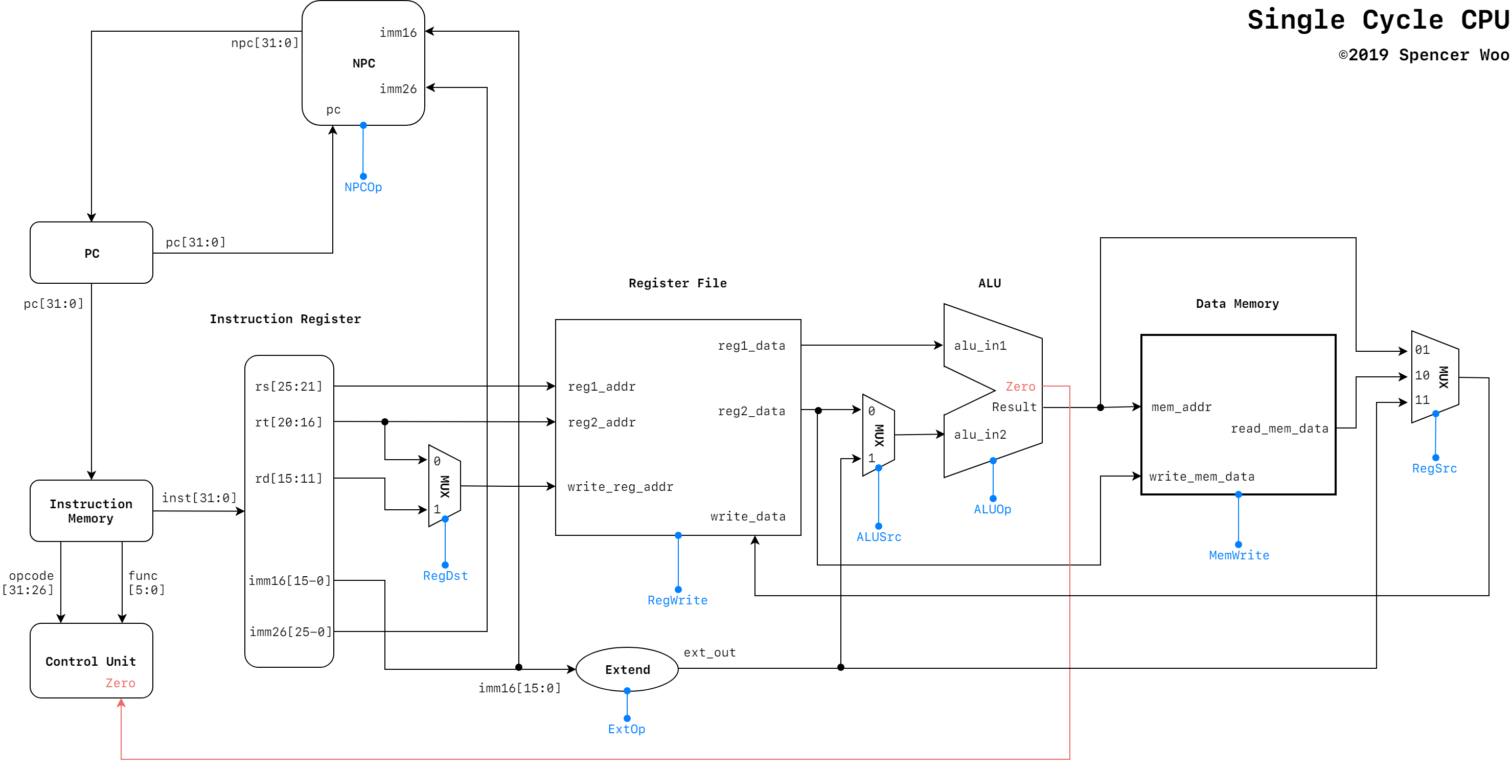
21 |
22 | Detailed documentation at: [🚡 Build Your PC - 个人项目 - 单周期 CPU](https://zanpu.spencerwoo.com/2_SingleCycle/2-1_Basic.html).
23 |
24 | ## Tests
25 |
26 | Complete simulated tests for the following instructions.
27 |
28 | ### LUI
29 |
30 | Test instructions:
31 |
32 | ```MIPS
33 | lui $1, 1
34 | lui $2, 2
35 | ```
36 |
37 | ```
38 |
39 | 0x3c010001
40 | 0x3c020002
41 | ```
42 |
43 | Expected:
44 |
45 | ```
46 |
47 | gpr[2] 00020000
48 | gpr[1] 00010000
49 | gpr[0] 00000000
50 | ```
51 |
52 | Results:
53 |
54 | 
55 |
56 | ### ADDIU
57 |
58 | Test instructions:
59 |
60 | ```MIPS
61 | lui $1, 1
62 | addiu $2, $1, 1024
63 | ```
64 |
65 | ```
66 |
67 | 0x3c010001
68 | 0x24220400
69 | ```
70 |
71 | Expected:
72 |
73 | ```
74 |
75 | gpr[2] 00010400
76 | gpr[1] 00010000
77 | gpr[0] 00000000
78 | ```
79 |
80 | Results:
81 |
82 | 
83 |
84 | ### ADD、SUBU
85 |
86 | Test instructions:
87 |
88 | ```MIPS
89 | lui $1, 1
90 | lui $2, 2
91 | add $3, $1, $2
92 | subu $4, $2, $1
93 | ```
94 |
95 | ```
96 |
97 | 0x3c010001
98 | 0x3c020002
99 | 0x00221820
100 | 0x00412023
101 | ```
102 |
103 | Expected:
104 |
105 | ```
106 |
107 | gpr[4] 00010000
108 | gpr[3] 00030000
109 | gpr[2] 00020000
110 | gpr[1] 00010000
111 | gpr[0] 00000000
112 | ```
113 |
114 | Results:
115 |
116 | 
117 |
118 | ### LW
119 |
120 | Test instructions:
121 |
122 | ```MIPS
123 | lw $1, 0
124 | lw $2, 4
125 | ```
126 |
127 | ```
128 |
129 | 0x8c010000
130 | 0x8c020004
131 | ```
132 |
133 | Initialize data memory with:
134 |
135 | ```
136 |
137 | 0x00000001
138 | 0x0000000f
139 | ```
140 |
141 | Expected:
142 |
143 | ```
144 |
145 | gpr[2] 0000000f
146 | gpr[1] 00000001
147 | gpr[0] 00000000
148 | ```
149 |
150 | Results:
151 |
152 | 
153 |
154 | ### SW
155 |
156 | Test instructions:
157 |
158 | ```MIPS
159 | addiu $1, $0, 0x0009
160 | sw $1, 8
161 | ```
162 |
163 | ```
164 |
165 | 0x24010009
166 | 0xac010008
167 | ```
168 |
169 | Expected:
170 |
171 | ```
172 |
173 | dm[2] 00000009
174 | dm[1] 0000000f
175 | dm[0] 00000001
176 | ```
177 |
178 | Results:
179 |
180 | 
181 |
182 | ### BEQ
183 |
184 | Test instructions:
185 |
186 | ```MIPS
187 | addiu $11, $0, 0x0009
188 | addiu $10, $0, 0x0009
189 | beq $11, $10, target
190 | lui $1, 1
191 | lui $2, 2
192 | target: lui $3, 3
193 | lui $4, 4
194 | ```
195 |
196 | ```
197 |
198 | 0x240b0009
199 | 0x240a0009
200 | 0x116a0002
201 | 0x3c010001
202 | 0x3c020002
203 | 0x3c030003
204 | 0x3c040004
205 | ```
206 |
207 | Expected:
208 |
209 | ```
210 |
211 | gpr[11] 00000009
212 | gpr[10] 00000009
213 | ...
214 | gpr[4] 00040000
215 | gpr[3] 00030000
216 | gpr[2] 00000000
217 | gpr[1] 00000000
218 | gpr[0] 00000000
219 | ```
220 |
221 | Results:
222 |
223 | 
224 |
225 | ### J
226 |
227 | Test instructions:
228 |
229 | ```MIPS
230 | j target
231 | lui $1, 1
232 | lui $2, 2
233 | target: lui $3, 3
234 | lui $4, 4
235 | ```
236 |
237 | ```
238 |
239 | 0x08100003
240 | 0x3c010001
241 | 0x3c020002
242 | 0x3c030003
243 | 0x3c040004
244 | ```
245 |
246 | Expected:
247 |
248 | ```
249 |
250 | gpr[4] 00040000
251 | gpr[3] 00030000
252 | gpr[2] 00000000
253 | gpr[1] 00000000
254 | gpr[0] 00000000
255 | ```
256 |
257 | Results:
258 |
259 | 
260 |
261 | ---
262 |
263 | 🎲 **Single Cycle CPU** ©Spencer Woo. Released under the [MIT License](./LICENSE).
264 |
265 | Authored and maintained by Spencer Woo.
266 |
267 | [@Portfolio](https://spencerwoo.com) · [@GitHub](https://github.com/spencerwooo) · [@BIT](http://www.bit.edu.cn/)
268 |
--------------------------------------------------------------------------------
/single-cycle-cpu.srcs/constrs_1/new/constraints.xdc:
--------------------------------------------------------------------------------
1 | set_property IOSTANDARD LVCMOS33 [get_ports {debug_reg_single[7]}]
2 | set_property IOSTANDARD LVCMOS33 [get_ports {debug_reg_single[6]}]
3 | set_property IOSTANDARD LVCMOS33 [get_ports {debug_reg_single[5]}]
4 | set_property IOSTANDARD LVCMOS33 [get_ports {debug_reg_single[4]}]
5 | set_property IOSTANDARD LVCMOS33 [get_ports {debug_reg_single[3]}]
6 | set_property IOSTANDARD LVCMOS33 [get_ports {debug_reg_single[2]}]
7 | set_property IOSTANDARD LVCMOS33 [get_ports {debug_reg_single[1]}]
8 | set_property IOSTANDARD LVCMOS33 [get_ports {debug_reg_single[0]}]
9 | set_property IOSTANDARD LVCMOS33 [get_ports clk]
10 | set_property IOSTANDARD LVCMOS33 [get_ports rst]
11 | set_property PACKAGE_PIN T5 [get_ports clk]
12 | set_property PACKAGE_PIN P15 [get_ports rst]
13 | set_property PACKAGE_PIN K2 [get_ports {debug_reg_single[0]}]
14 | set_property PACKAGE_PIN J2 [get_ports {debug_reg_single[1]}]
15 | set_property PACKAGE_PIN J3 [get_ports {debug_reg_single[2]}]
16 | set_property PACKAGE_PIN H4 [get_ports {debug_reg_single[3]}]
17 | set_property PACKAGE_PIN J4 [get_ports {debug_reg_single[4]}]
18 | set_property PACKAGE_PIN G3 [get_ports {debug_reg_single[5]}]
19 | set_property PACKAGE_PIN G4 [get_ports {debug_reg_single[6]}]
20 | set_property PACKAGE_PIN F6 [get_ports {debug_reg_single[7]}]
21 |
--------------------------------------------------------------------------------
/single-cycle-cpu.srcs/sim_1/new/testbench.v:
--------------------------------------------------------------------------------
1 | `timescale 1ns / 1ps
2 |
3 | /*
4 | * Testbench
5 | */
6 |
7 | module testbench();
8 | reg clk;
9 | reg rst;
10 | top ZAN_TOP(clk, rst);
11 |
12 | initial begin
13 | // // Load instructions
14 | // $readmemh("../../../tests/instructions.txt", ZAN_TOP.ZAN_INSTR_MEM.im);
15 | // // Load register initial values
16 | // $readmemh("../../../tests/register.txt", ZAN_TOP.ZAN_REG_FILE.gpr);
17 | // // Load memory data initial values
18 | // $readmemh("../../../tests/data_memory.txt", ZAN_TOP.ZAN_DATA_MEM.dm);
19 |
20 | rst = 1;
21 | clk = 0;
22 |
23 | #30 rst = 0;
24 | // #80 $display("$10 value: %h", ZAN_TOP.ZAN_REG_FILE.gpr[10]);
25 | #500 $stop;
26 | end
27 |
28 | always
29 | #20 clk = ~clk;
30 | endmodule
31 |
--------------------------------------------------------------------------------
/single-cycle-cpu.srcs/sources_1/ip/data_memory_ip/data_memory_ip.dcp:
--------------------------------------------------------------------------------
https://raw.githubusercontent.com/spencerwooo/single-cycle-processor/63187f355459f5d1482f4a53c7116b2c8a4080d1/single-cycle-cpu.srcs/sources_1/ip/data_memory_ip/data_memory_ip.dcp
--------------------------------------------------------------------------------
/single-cycle-cpu.srcs/sources_1/ip/data_memory_ip/data_memory_ip.mif:
--------------------------------------------------------------------------------
1 | 00000000000000000000000000000000
2 | 00000000000000000000000000000000
3 | 00000000000000000000000000000000
4 |
--------------------------------------------------------------------------------
/single-cycle-cpu.srcs/sources_1/ip/data_memory_ip/data_memory_ip.veo:
--------------------------------------------------------------------------------
1 | // (c) Copyright 1995-2019 Xilinx, Inc. All rights reserved.
2 | //
3 | // This file contains confidential and proprietary information
4 | // of Xilinx, Inc. and is protected under U.S. and
5 | // international copyright and other intellectual property
6 | // laws.
7 | //
8 | // DISCLAIMER
9 | // This disclaimer is not a license and does not grant any
10 | // rights to the materials distributed herewith. Except as
11 | // otherwise provided in a valid license issued to you by
12 | // Xilinx, and to the maximum extent permitted by applicable
13 | // law: (1) THESE MATERIALS ARE MADE AVAILABLE "AS IS" AND
14 | // WITH ALL FAULTS, AND XILINX HEREBY DISCLAIMS ALL WARRANTIES
15 | // AND CONDITIONS, EXPRESS, IMPLIED, OR STATUTORY, INCLUDING
16 | // BUT NOT LIMITED TO WARRANTIES OF MERCHANTABILITY, NON-
17 | // INFRINGEMENT, OR FITNESS FOR ANY PARTICULAR PURPOSE; and
18 | // (2) Xilinx shall not be liable (whether in contract or tort,
19 | // including negligence, or under any other theory of
20 | // liability) for any loss or damage of any kind or nature
21 | // related to, arising under or in connection with these
22 | // materials, including for any direct, or any indirect,
23 | // special, incidental, or consequential loss or damage
24 | // (including loss of data, profits, goodwill, or any type of
25 | // loss or damage suffered as a result of any action brought
26 | // by a third party) even if such damage or loss was
27 | // reasonably foreseeable or Xilinx had been advised of the
28 | // possibility of the same.
29 | //
30 | // CRITICAL APPLICATIONS
31 | // Xilinx products are not designed or intended to be fail-
32 | // safe, or for use in any application requiring fail-safe
33 | // performance, such as life-support or safety devices or
34 | // systems, Class III medical devices, nuclear facilities,
35 | // applications related to the deployment of airbags, or any
36 | // other applications that could lead to death, personal
37 | // injury, or severe property or environmental damage
38 | // (individually and collectively, "Critical
39 | // Applications"). Customer assumes the sole risk and
40 | // liability of any use of Xilinx products in Critical
41 | // Applications, subject only to applicable laws and
42 | // regulations governing limitations on product liability.
43 | //
44 | // THIS COPYRIGHT NOTICE AND DISCLAIMER MUST BE RETAINED AS
45 | // PART OF THIS FILE AT ALL TIMES.
46 | //
47 | // DO NOT MODIFY THIS FILE.
48 |
49 | // IP VLNV: xilinx.com:ip:dist_mem_gen:8.0
50 | // IP Revision: 11
51 |
52 | // The following must be inserted into your Verilog file for this
53 | // core to be instantiated. Change the instance name and port connections
54 | // (in parentheses) to your own signal names.
55 |
56 | //----------- Begin Cut here for INSTANTIATION Template ---// INST_TAG
57 | data_memory_ip your_instance_name (
58 | .a(a), // input wire [9 : 0] a
59 | .d(d), // input wire [31 : 0] d
60 | .clk(clk), // input wire clk
61 | .we(we), // input wire we
62 | .spo(spo) // output wire [31 : 0] spo
63 | );
64 | // INST_TAG_END ------ End INSTANTIATION Template ---------
65 |
66 | // You must compile the wrapper file data_memory_ip.v when simulating
67 | // the core, data_memory_ip. When compiling the wrapper file, be sure to
68 | // reference the Verilog simulation library.
69 |
70 |
--------------------------------------------------------------------------------
/single-cycle-cpu.srcs/sources_1/ip/data_memory_ip/data_memory_ip.vho:
--------------------------------------------------------------------------------
1 | -- (c) Copyright 1995-2019 Xilinx, Inc. All rights reserved.
2 | --
3 | -- This file contains confidential and proprietary information
4 | -- of Xilinx, Inc. and is protected under U.S. and
5 | -- international copyright and other intellectual property
6 | -- laws.
7 | --
8 | -- DISCLAIMER
9 | -- This disclaimer is not a license and does not grant any
10 | -- rights to the materials distributed herewith. Except as
11 | -- otherwise provided in a valid license issued to you by
12 | -- Xilinx, and to the maximum extent permitted by applicable
13 | -- law: (1) THESE MATERIALS ARE MADE AVAILABLE "AS IS" AND
14 | -- WITH ALL FAULTS, AND XILINX HEREBY DISCLAIMS ALL WARRANTIES
15 | -- AND CONDITIONS, EXPRESS, IMPLIED, OR STATUTORY, INCLUDING
16 | -- BUT NOT LIMITED TO WARRANTIES OF MERCHANTABILITY, NON-
17 | -- INFRINGEMENT, OR FITNESS FOR ANY PARTICULAR PURPOSE; and
18 | -- (2) Xilinx shall not be liable (whether in contract or tort,
19 | -- including negligence, or under any other theory of
20 | -- liability) for any loss or damage of any kind or nature
21 | -- related to, arising under or in connection with these
22 | -- materials, including for any direct, or any indirect,
23 | -- special, incidental, or consequential loss or damage
24 | -- (including loss of data, profits, goodwill, or any type of
25 | -- loss or damage suffered as a result of any action brought
26 | -- by a third party) even if such damage or loss was
27 | -- reasonably foreseeable or Xilinx had been advised of the
28 | -- possibility of the same.
29 | --
30 | -- CRITICAL APPLICATIONS
31 | -- Xilinx products are not designed or intended to be fail-
32 | -- safe, or for use in any application requiring fail-safe
33 | -- performance, such as life-support or safety devices or
34 | -- systems, Class III medical devices, nuclear facilities,
35 | -- applications related to the deployment of airbags, or any
36 | -- other applications that could lead to death, personal
37 | -- injury, or severe property or environmental damage
38 | -- (individually and collectively, "Critical
39 | -- Applications"). Customer assumes the sole risk and
40 | -- liability of any use of Xilinx products in Critical
41 | -- Applications, subject only to applicable laws and
42 | -- regulations governing limitations on product liability.
43 | --
44 | -- THIS COPYRIGHT NOTICE AND DISCLAIMER MUST BE RETAINED AS
45 | -- PART OF THIS FILE AT ALL TIMES.
46 | --
47 | -- DO NOT MODIFY THIS FILE.
48 |
49 | -- IP VLNV: xilinx.com:ip:dist_mem_gen:8.0
50 | -- IP Revision: 11
51 |
52 | -- The following code must appear in the VHDL architecture header.
53 |
54 | ------------- Begin Cut here for COMPONENT Declaration ------ COMP_TAG
55 | COMPONENT data_memory_ip
56 | PORT (
57 | a : IN STD_LOGIC_VECTOR(9 DOWNTO 0);
58 | d : IN STD_LOGIC_VECTOR(31 DOWNTO 0);
59 | clk : IN STD_LOGIC;
60 | we : IN STD_LOGIC;
61 | spo : OUT STD_LOGIC_VECTOR(31 DOWNTO 0)
62 | );
63 | END COMPONENT;
64 | -- COMP_TAG_END ------ End COMPONENT Declaration ------------
65 |
66 | -- The following code must appear in the VHDL architecture
67 | -- body. Substitute your own instance name and net names.
68 |
69 | ------------- Begin Cut here for INSTANTIATION Template ----- INST_TAG
70 | your_instance_name : data_memory_ip
71 | PORT MAP (
72 | a => a,
73 | d => d,
74 | clk => clk,
75 | we => we,
76 | spo => spo
77 | );
78 | -- INST_TAG_END ------ End INSTANTIATION Template ---------
79 |
80 | -- You must compile the wrapper file data_memory_ip.vhd when simulating
81 | -- the core, data_memory_ip. When compiling the wrapper file, be sure to
82 | -- reference the VHDL simulation library.
83 |
84 |
--------------------------------------------------------------------------------
/single-cycle-cpu.srcs/sources_1/ip/data_memory_ip/data_memory_ip.xci:
--------------------------------------------------------------------------------
1 |
2 |
3 | xilinx.com
4 | xci
5 | unknown
6 | 1.0
7 |
8 |
9 | data_memory_ip
10 |
11 |
12 | 10
13 | 0
14 | 1024
15 | ./
16 | artix7
17 | 1
18 | 1
19 | 0
20 | 0
21 | 0
22 | 0
23 | 0
24 | 0
25 | 0
26 | 0
27 | 0
28 | 0
29 | 0
30 | 0
31 | 1
32 | 1
33 | data_memory_ip.mif
34 | 1
35 | 1
36 | 0
37 | 0
38 | 0
39 | 1
40 | 0
41 | 0
42 | 1
43 | 32
44 | data_memory_ip
45 | 0
46 | ce_overrides_sync_controls
47 | ../../../../tests/data_memory_tests.coe
48 | false
49 | false
50 | 32
51 | 0
52 | 16
53 | 1024
54 | non_registered
55 | false
56 | false
57 | non_registered
58 | single_port_ram
59 | non_registered
60 | false
61 | false
62 | false
63 | false
64 | non_registered
65 | false
66 | false
67 | false
68 | false
69 | false
70 | artix7
71 |
72 | xc7a35t
73 | csg324
74 | VERILOG
75 |
76 | MIXED
77 | -1
78 |
79 | TRUE
80 | TRUE
81 | IP_Flow
82 | 11
83 | TRUE
84 | .
85 |
86 | .
87 | 2017.2
88 | OUT_OF_CONTEXT
89 |
90 |
91 |
92 |
93 |
94 |
95 |
96 |
97 |
98 |
99 |
100 |
101 |
102 |
--------------------------------------------------------------------------------
/single-cycle-cpu.srcs/sources_1/ip/data_memory_ip/data_memory_ip_ooc.xdc:
--------------------------------------------------------------------------------
1 | ################################################################################
2 | #
3 | # (c) Copyright 2009 - 2014 Xilinx, Inc. All rights reserved.
4 | #
5 | # This file contains confidential and proprietary information
6 | # of Xilinx, Inc. and is protected under U.S. and
7 | # international copyright and other intellectual property
8 | # laws.
9 | #
10 | # DISCLAIMER
11 | # This disclaimer is not a license and does not grant any
12 | # rights to the materials distributed herewith. Except as
13 | # otherwise provided in a valid license issued to you by
14 | # Xilinx, and to the maximum extent permitted by applicable
15 | # law: (1) THESE MATERIALS ARE MADE AVAILABLE "AS IS" AND
16 | # WITH ALL FAULTS, AND XILINX HEREBY DISCLAIMS ALL WARRANTIES
17 | # AND CONDITIONS, EXPRESS, IMPLIED, OR STATUTORY, INCLUDING
18 | # BUT NOT LIMITED TO WARRANTIES OF MERCHANTABILITY, NON-
19 | # INFRINGEMENT, OR FITNESS FOR ANY PARTICULAR PURPOSE; and
20 | # (2) Xilinx shall not be liable (whether in contract or tort,
21 | # including negligence, or under any other theory of
22 | # liability) for any loss or damage of any kind or nature
23 | # related to, arising under or in connection with these
24 | # materials, including for any direct, or any indirect,
25 | # special, incidental, or consequential loss or damage
26 | # (including loss of data, profits, goodwill, or any type of
27 | # loss or damage suffered as a result of any action brought
28 | # by a third party) even if such damage or loss was
29 | # reasonably foreseeable or Xilinx had been advised of the
30 | # possibility of the same.
31 | #
32 | # CRITICAL APPLICATIONS
33 | # Xilinx products are not designed or intended to be fail-
34 | # safe, or for use in any application requiring fail-safe
35 | # performance, such as life-support or safety devices or
36 | # systems, Class III medical devices, nuclear facilities,
37 | # applications related to the deployment of airbags, or any
38 | # other applications that could lead to death, personal
39 | # injury, or severe property or environmental damage
40 | # (individually and collectively, "Critical
41 | # Applications"). Customer assumes the sole risk and
42 | # liability of any use of Xilinx products in Critical
43 | # Applications, subject only to applicable laws and
44 | # regulations governing limitations on product liability.
45 | #
46 | # THIS COPYRIGHT NOTICE AND DISCLAIMER MUST BE RETAINED AS
47 | # PART OF THIS FILE AT ALL TIMES.
48 | #
49 | ################################################################################
50 |
51 | # Tx Core Period Constraint. This constraint can be modified, and is
52 | # valid as long as it is met after place and route.
53 | create_clock -name "TS_CLK" -period 20.0 [ get_ports clk ]
54 |
55 |
56 | ################################################################################
57 |
--------------------------------------------------------------------------------
/single-cycle-cpu.srcs/sources_1/ip/data_memory_ip/data_memory_ip_stub.v:
--------------------------------------------------------------------------------
1 | // Copyright 1986-2017 Xilinx, Inc. All Rights Reserved.
2 | // --------------------------------------------------------------------------------
3 | // Tool Version: Vivado v.2017.2 (win64) Build 1909853 Thu Jun 15 18:39:09 MDT 2017
4 | // Date : Sun Sep 15 15:45:21 2019
5 | // Host : DESKTOP-IT0A8CI running 64-bit major release (build 9200)
6 | // Command : write_verilog -force -mode synth_stub -rename_top data_memory_ip -prefix
7 | // data_memory_ip_ data_memory_ip_stub.v
8 | // Design : data_memory_ip
9 | // Purpose : Stub declaration of top-level module interface
10 | // Device : xc7a35tcsg324-1
11 | // --------------------------------------------------------------------------------
12 |
13 | // This empty module with port declaration file causes synthesis tools to infer a black box for IP.
14 | // The synthesis directives are for Synopsys Synplify support to prevent IO buffer insertion.
15 | // Please paste the declaration into a Verilog source file or add the file as an additional source.
16 | (* x_core_info = "dist_mem_gen_v8_0_11,Vivado 2017.2" *)
17 | module data_memory_ip(a, d, clk, we, spo)
18 | /* synthesis syn_black_box black_box_pad_pin="a[9:0],d[31:0],clk,we,spo[31:0]" */;
19 | input [9:0]a;
20 | input [31:0]d;
21 | input clk;
22 | input we;
23 | output [31:0]spo;
24 | endmodule
25 |
--------------------------------------------------------------------------------
/single-cycle-cpu.srcs/sources_1/ip/data_memory_ip/data_memory_ip_stub.vhdl:
--------------------------------------------------------------------------------
1 | -- Copyright 1986-2017 Xilinx, Inc. All Rights Reserved.
2 | -- --------------------------------------------------------------------------------
3 | -- Tool Version: Vivado v.2017.2 (win64) Build 1909853 Thu Jun 15 18:39:09 MDT 2017
4 | -- Date : Sun Sep 15 15:45:21 2019
5 | -- Host : DESKTOP-IT0A8CI running 64-bit major release (build 9200)
6 | -- Command : write_vhdl -force -mode synth_stub -rename_top data_memory_ip -prefix
7 | -- data_memory_ip_ data_memory_ip_stub.vhdl
8 | -- Design : data_memory_ip
9 | -- Purpose : Stub declaration of top-level module interface
10 | -- Device : xc7a35tcsg324-1
11 | -- --------------------------------------------------------------------------------
12 | library IEEE;
13 | use IEEE.STD_LOGIC_1164.ALL;
14 |
15 | entity data_memory_ip is
16 | Port (
17 | a : in STD_LOGIC_VECTOR ( 9 downto 0 );
18 | d : in STD_LOGIC_VECTOR ( 31 downto 0 );
19 | clk : in STD_LOGIC;
20 | we : in STD_LOGIC;
21 | spo : out STD_LOGIC_VECTOR ( 31 downto 0 )
22 | );
23 |
24 | end data_memory_ip;
25 |
26 | architecture stub of data_memory_ip is
27 | attribute syn_black_box : boolean;
28 | attribute black_box_pad_pin : string;
29 | attribute syn_black_box of stub : architecture is true;
30 | attribute black_box_pad_pin of stub : architecture is "a[9:0],d[31:0],clk,we,spo[31:0]";
31 | attribute x_core_info : string;
32 | attribute x_core_info of stub : architecture is "dist_mem_gen_v8_0_11,Vivado 2017.2";
33 | begin
34 | end;
35 |
--------------------------------------------------------------------------------
/single-cycle-cpu.srcs/sources_1/ip/data_memory_ip/doc/dist_mem_gen_v8_0_changelog.txt:
--------------------------------------------------------------------------------
1 | 2017.2:
2 | * Version 8.0 (Rev. 11)
3 | * No changes
4 |
5 | 2017.1:
6 | * Version 8.0 (Rev. 11)
7 | * No changes
8 |
9 | 2016.4:
10 | * Version 8.0 (Rev. 11)
11 | * No changes
12 |
13 | 2016.3:
14 | * Version 8.0 (Rev. 11)
15 | * General: Enable support for future devices
16 |
17 | 2016.2:
18 | * Version 8.0 (Rev. 10)
19 | * No changes
20 |
21 | 2016.1:
22 | * Version 8.0 (Rev. 10)
23 | * Delivering only verilog simulation model, Stopped delivery of vhdl simulation model.
24 |
25 | 2015.4.2:
26 | * Version 8.0 (Rev. 9)
27 | * No changes
28 |
29 | 2015.4.1:
30 | * Version 8.0 (Rev. 9)
31 | * No changes
32 |
33 | 2015.4:
34 | * Version 8.0 (Rev. 9)
35 | * No changes
36 |
37 | 2015.3:
38 | * Version 8.0 (Rev. 9)
39 | * Delivering only vhdl simulation model, Stopped delivery of verilog simulation model.
40 | * IP revision number added to HDL module, library, and include file names, to support designs with both locked and upgraded IP instances
41 |
42 | 2015.2.1:
43 | * Version 8.0 (Rev. 8)
44 | * No changes
45 |
46 | 2015.2:
47 | * Version 8.0 (Rev. 8)
48 | * No changes
49 |
50 | 2015.1:
51 | * Version 8.0 (Rev. 8)
52 | * Delivering unencrypted simulation files.
53 | * Supported devices and production status are now determined automatically, to simplify support for future devices
54 |
55 | 2014.4.1:
56 | * Version 8.0 (Rev. 7)
57 | * No changes
58 |
59 | 2014.4:
60 | * Version 8.0 (Rev. 7)
61 | * Encrypted source files are concatenated together to reduce the number of files and to reduce simulator compile time
62 | * Internal device family change, no functional changes
63 |
64 | 2014.3:
65 | * Version 8.0 (Rev. 6)
66 | * Reduced warnings in synthesis, no functional changes
67 |
68 | 2014.2:
69 | * Version 8.0 (Rev. 5)
70 | * Repackaged to improve internal automation, no functional changes.
71 |
72 | 2014.1:
73 | * Version 8.0 (Rev. 4)
74 | * Internal device family name change, no functional changes
75 |
76 | 2013.4:
77 | * Version 8.0 (Rev. 3)
78 | * Added support for Ultrascale devices
79 |
80 | 2013.3:
81 | * Version 8.0 (Rev. 2)
82 | * Enhanced support for IP Integrator
83 | * Reduced warnings in synthesis and simulation
84 | * Added support for Cadence IES and Synopsys VCS simulators
85 |
86 | 2013.2:
87 | * Version 8.0 (Rev. 1)
88 | * Repackaged to enable internal version management, no functional changes.
89 |
90 | 2013.1:
91 | * Version 8.0
92 | * Native Vivado Release
93 | * Unused port SPRA and its associated parameters removed.
94 |
95 | (c) Copyright 2002 - 2017 Xilinx, Inc. All rights reserved.
96 |
97 | This file contains confidential and proprietary information
98 | of Xilinx, Inc. and is protected under U.S. and
99 | international copyright and other intellectual property
100 | laws.
101 |
102 | DISCLAIMER
103 | This disclaimer is not a license and does not grant any
104 | rights to the materials distributed herewith. Except as
105 | otherwise provided in a valid license issued to you by
106 | Xilinx, and to the maximum extent permitted by applicable
107 | law: (1) THESE MATERIALS ARE MADE AVAILABLE "AS IS" AND
108 | WITH ALL FAULTS, AND XILINX HEREBY DISCLAIMS ALL WARRANTIES
109 | AND CONDITIONS, EXPRESS, IMPLIED, OR STATUTORY, INCLUDING
110 | BUT NOT LIMITED TO WARRANTIES OF MERCHANTABILITY, NON-
111 | INFRINGEMENT, OR FITNESS FOR ANY PARTICULAR PURPOSE; and
112 | (2) Xilinx shall not be liable (whether in contract or tort,
113 | including negligence, or under any other theory of
114 | liability) for any loss or damage of any kind or nature
115 | related to, arising under or in connection with these
116 | materials, including for any direct, or any indirect,
117 | special, incidental, or consequential loss or damage
118 | (including loss of data, profits, goodwill, or any type of
119 | loss or damage suffered as a result of any action brought
120 | by a third party) even if such damage or loss was
121 | reasonably foreseeable or Xilinx had been advised of the
122 | possibility of the same.
123 |
124 | CRITICAL APPLICATIONS
125 | Xilinx products are not designed or intended to be fail-
126 | safe, or for use in any application requiring fail-safe
127 | performance, such as life-support or safety devices or
128 | systems, Class III medical devices, nuclear facilities,
129 | applications related to the deployment of airbags, or any
130 | other applications that could lead to death, personal
131 | injury, or severe property or environmental damage
132 | (individually and collectively, "Critical
133 | Applications"). Customer assumes the sole risk and
134 | liability of any use of Xilinx products in Critical
135 | Applications, subject only to applicable laws and
136 | regulations governing limitations on product liability.
137 |
138 | THIS COPYRIGHT NOTICE AND DISCLAIMER MUST BE RETAINED AS
139 | PART OF THIS FILE AT ALL TIMES.
140 |
--------------------------------------------------------------------------------
/single-cycle-cpu.srcs/sources_1/ip/data_memory_ip/sim/data_memory_ip.v:
--------------------------------------------------------------------------------
1 | // (c) Copyright 1995-2019 Xilinx, Inc. All rights reserved.
2 | //
3 | // This file contains confidential and proprietary information
4 | // of Xilinx, Inc. and is protected under U.S. and
5 | // international copyright and other intellectual property
6 | // laws.
7 | //
8 | // DISCLAIMER
9 | // This disclaimer is not a license and does not grant any
10 | // rights to the materials distributed herewith. Except as
11 | // otherwise provided in a valid license issued to you by
12 | // Xilinx, and to the maximum extent permitted by applicable
13 | // law: (1) THESE MATERIALS ARE MADE AVAILABLE "AS IS" AND
14 | // WITH ALL FAULTS, AND XILINX HEREBY DISCLAIMS ALL WARRANTIES
15 | // AND CONDITIONS, EXPRESS, IMPLIED, OR STATUTORY, INCLUDING
16 | // BUT NOT LIMITED TO WARRANTIES OF MERCHANTABILITY, NON-
17 | // INFRINGEMENT, OR FITNESS FOR ANY PARTICULAR PURPOSE; and
18 | // (2) Xilinx shall not be liable (whether in contract or tort,
19 | // including negligence, or under any other theory of
20 | // liability) for any loss or damage of any kind or nature
21 | // related to, arising under or in connection with these
22 | // materials, including for any direct, or any indirect,
23 | // special, incidental, or consequential loss or damage
24 | // (including loss of data, profits, goodwill, or any type of
25 | // loss or damage suffered as a result of any action brought
26 | // by a third party) even if such damage or loss was
27 | // reasonably foreseeable or Xilinx had been advised of the
28 | // possibility of the same.
29 | //
30 | // CRITICAL APPLICATIONS
31 | // Xilinx products are not designed or intended to be fail-
32 | // safe, or for use in any application requiring fail-safe
33 | // performance, such as life-support or safety devices or
34 | // systems, Class III medical devices, nuclear facilities,
35 | // applications related to the deployment of airbags, or any
36 | // other applications that could lead to death, personal
37 | // injury, or severe property or environmental damage
38 | // (individually and collectively, "Critical
39 | // Applications"). Customer assumes the sole risk and
40 | // liability of any use of Xilinx products in Critical
41 | // Applications, subject only to applicable laws and
42 | // regulations governing limitations on product liability.
43 | //
44 | // THIS COPYRIGHT NOTICE AND DISCLAIMER MUST BE RETAINED AS
45 | // PART OF THIS FILE AT ALL TIMES.
46 | //
47 | // DO NOT MODIFY THIS FILE.
48 |
49 |
50 | // IP VLNV: xilinx.com:ip:dist_mem_gen:8.0
51 | // IP Revision: 11
52 |
53 | `timescale 1ns/1ps
54 |
55 | (* DowngradeIPIdentifiedWarnings = "yes" *)
56 | module data_memory_ip (
57 | a,
58 | d,
59 | clk,
60 | we,
61 | spo
62 | );
63 |
64 | input wire [9 : 0] a;
65 | input wire [31 : 0] d;
66 | input wire clk;
67 | input wire we;
68 | output wire [31 : 0] spo;
69 |
70 | dist_mem_gen_v8_0_11 #(
71 | .C_FAMILY("artix7"),
72 | .C_ADDR_WIDTH(10),
73 | .C_DEFAULT_DATA("0"),
74 | .C_DEPTH(1024),
75 | .C_HAS_CLK(1),
76 | .C_HAS_D(1),
77 | .C_HAS_DPO(0),
78 | .C_HAS_DPRA(0),
79 | .C_HAS_I_CE(0),
80 | .C_HAS_QDPO(0),
81 | .C_HAS_QDPO_CE(0),
82 | .C_HAS_QDPO_CLK(0),
83 | .C_HAS_QDPO_RST(0),
84 | .C_HAS_QDPO_SRST(0),
85 | .C_HAS_QSPO(0),
86 | .C_HAS_QSPO_CE(0),
87 | .C_HAS_QSPO_RST(0),
88 | .C_HAS_QSPO_SRST(0),
89 | .C_HAS_SPO(1),
90 | .C_HAS_WE(1),
91 | .C_MEM_INIT_FILE("data_memory_ip.mif"),
92 | .C_ELABORATION_DIR("./"),
93 | .C_MEM_TYPE(1),
94 | .C_PIPELINE_STAGES(0),
95 | .C_QCE_JOINED(0),
96 | .C_QUALIFY_WE(0),
97 | .C_READ_MIF(1),
98 | .C_REG_A_D_INPUTS(0),
99 | .C_REG_DPRA_INPUT(0),
100 | .C_SYNC_ENABLE(1),
101 | .C_WIDTH(32),
102 | .C_PARSER_TYPE(1)
103 | ) inst (
104 | .a(a),
105 | .d(d),
106 | .dpra(10'B0),
107 | .clk(clk),
108 | .we(we),
109 | .i_ce(1'D1),
110 | .qspo_ce(1'D1),
111 | .qdpo_ce(1'D1),
112 | .qdpo_clk(1'D0),
113 | .qspo_rst(1'D0),
114 | .qdpo_rst(1'D0),
115 | .qspo_srst(1'D0),
116 | .qdpo_srst(1'D0),
117 | .spo(spo),
118 | .dpo(),
119 | .qspo(),
120 | .qdpo()
121 | );
122 | endmodule
123 |
--------------------------------------------------------------------------------
/single-cycle-cpu.srcs/sources_1/ip/data_memory_ip/simulation/dist_mem_gen_v8_0.v:
--------------------------------------------------------------------------------
1 | /*
2 | *******************************************************************************
3 | *
4 | * Distributed Memory Generator - Verilog Behavioral Model
5 | *
6 | *******************************************************************************
7 | *
8 | * (c) Copyright 1995 - 2009 Xilinx, Inc. All rights reserved.
9 | *
10 | * This file contains confidential and proprietary information
11 | * of Xilinx, Inc. and is protected under U.S. and
12 | * international copyright and other intellectual property
13 | * laws.
14 | *
15 | * DISCLAIMER
16 | * This disclaimer is not a license and does not grant any
17 | * rights to the materials distributed herewith. Except as
18 | * otherwise provided in a valid license issued to you by
19 | * Xilinx, and to the maximum extent permitted by applicable
20 | * law: (1) THESE MATERIALS ARE MADE AVAILABLE "AS IS" AND
21 | * WITH ALL FAULTS, AND XILINX HEREBY DISCLAIMS ALL WARRANTIES
22 | * AND CONDITIONS, EXPRESS, IMPLIED, OR STATUTORY, INCLUDING
23 | * BUT NOT LIMITED TO WARRANTIES OF MERCHANTABILITY, NON-
24 | * INFRINGEMENT, OR FITNESS FOR ANY PARTICULAR PURPOSE; and
25 | * (2) Xilinx shall not be liable (whether in contract or tort,
26 | * including negligence, or under any other theory of
27 | * liability) for any loss or damage of any kind or nature
28 | * related to, arising under or in connection with these
29 | * materials, including for any direct, or any indirect,
30 | * special, incidental, or consequential loss or damage
31 | * (including loss of data, profits, goodwill, or any type of
32 | * loss or damage suffered as a result of any action brought
33 | * by a third party) even if such damage or loss was
34 | * reasonably foreseeable or Xilinx had been advised of the
35 | * possibility of the same.
36 | *
37 | * CRITICAL APPLICATIONS
38 | * Xilinx products are not designed or intended to be fail-
39 | * safe, or for use in any application requiring fail-safe
40 | * performance, such as life-support or safety devices or
41 | * systems, Class III medical devices, nuclear facilities,
42 | * applications related to the deployment of airbags, or any
43 | * other applications that could lead to death, personal
44 | * injury, or severe property or environmental damage
45 | * (individually and collectively, "Critical
46 | * Applications"). Customer assumes the sole risk and
47 | * liability of any use of Xilinx products in Critical
48 | * Applications, subject only to applicable laws and
49 | * regulations governing limitations on product liability.
50 | *
51 | * THIS COPYRIGHT NOTICE AND DISCLAIMER MUST BE RETAINED AS
52 | * PART OF THIS FILE AT ALL TIMES.
53 | *
54 | *******************************************************************************
55 | *******************************************************************************
56 | *
57 | * Filename : dist_mem_gen_v8_0_11.v
58 | *
59 | * Author : Xilinx
60 | *
61 | * Description : Distributed Memory Simulation Model
62 | *
63 | *******************************************************************************
64 | */
65 |
66 | `timescale 1ps/1ps
67 | `ifndef TCQ
68 | `define TCQ 100
69 | `endif
70 |
71 | `define all0s {C_WIDTH{1'b0}}
72 | `define allXs {C_WIDTH{1'bx}}
73 | `define c_rom 0
74 | `define c_sp_ram 1
75 | `define c_dp_ram 2
76 | `define c_sdp_ram 4
77 |
78 | module dist_mem_gen_v8_0_11 (a, d, dpra, clk, we, i_ce, qspo_ce, qdpo_ce, qdpo_clk, qspo_rst, qdpo_rst, qspo_srst, qdpo_srst, spo, dpo, qspo, qdpo);
79 |
80 | parameter C_FAMILY = "virtex5";
81 | parameter C_ADDR_WIDTH = 6;
82 | parameter C_DEFAULT_DATA = "0";
83 | parameter C_ELABORATION_DIR = "./";
84 | parameter C_DEPTH = 64;
85 | parameter C_HAS_CLK = 1;
86 | parameter C_HAS_D = 1;
87 | parameter C_HAS_DPO = 0;
88 | parameter C_HAS_DPRA = 0;
89 | parameter C_HAS_I_CE = 0;
90 | parameter C_HAS_QDPO = 0;
91 | parameter C_HAS_QDPO_CE = 0;
92 | parameter C_HAS_QDPO_CLK = 0;
93 | parameter C_HAS_QDPO_RST = 0;
94 | parameter C_HAS_QDPO_SRST = 0;
95 | parameter C_HAS_QSPO = 0;
96 | parameter C_HAS_QSPO_CE = 0;
97 | parameter C_HAS_QSPO_RST = 0;
98 | parameter C_HAS_QSPO_SRST = 0;
99 | parameter C_HAS_SPO = 1;
100 | parameter C_HAS_WE = 1;
101 | parameter C_MEM_INIT_FILE = "null.mif";
102 | parameter C_MEM_TYPE = 1;
103 | parameter C_PIPELINE_STAGES = 0;
104 | parameter C_QCE_JOINED = 0;
105 | parameter C_QUALIFY_WE = 0;
106 | parameter C_READ_MIF = 0;
107 | parameter C_REG_A_D_INPUTS = 0;
108 | parameter C_REG_DPRA_INPUT = 0;
109 | parameter C_SYNC_ENABLE = 0;
110 | parameter C_WIDTH = 16;
111 | parameter C_PARSER_TYPE = 1;
112 |
113 | input [C_ADDR_WIDTH-1:0] a;
114 | input [C_WIDTH-1 : 0] d;
115 | input [C_ADDR_WIDTH-1 : 0] dpra;
116 | input clk;
117 | input we;
118 | input i_ce;
119 | input qspo_ce;
120 | input qdpo_ce;
121 | input qdpo_clk;
122 | input qspo_rst;
123 | input qdpo_rst;
124 | input qspo_srst;
125 | input qdpo_srst;
126 | output [C_WIDTH-1 : 0] spo;
127 | output [C_WIDTH-1 : 0] qspo;
128 | output [C_WIDTH-1 : 0] dpo;
129 | output [C_WIDTH-1 : 0] qdpo;
130 |
131 | // Address signal connected to memory
132 | wire [C_ADDR_WIDTH - 1 : 0] a_int;
133 |
134 | // Input data signal connected to memory
135 | wire [C_WIDTH - 1 : 0] d_int;
136 |
137 | // Internal Write Enable
138 | wire we_int;
139 |
140 | // Internal QSPO Clock Enable
141 | wire qspo_ce_int;
142 |
143 | // Internal QDPO Clock
144 | wire qdpo_clk_int;
145 |
146 | // Internal Dual Port Read Address connected to memory
147 | wire [C_ADDR_WIDTH - 1 : 0] dpra_int;
148 |
149 | // Internal QDPO Clock Enable
150 | wire qdpo_ce_int;
151 |
152 | // Registered Write Enable
153 | reg we_reg;
154 |
155 | // Registered Address connected to memory
156 | reg [C_ADDR_WIDTH - 1 : 0] a_reg;
157 |
158 | // Registered data signal connected to memory
159 | reg [C_WIDTH-1 : 0] d_reg;
160 |
161 | // Registered QSPO Clock Enable
162 | reg qspo_ce_reg;
163 |
164 | // Registered Dual Port Read Address connected to memory
165 | reg [C_ADDR_WIDTH - 1 : 0] dpra_reg;
166 |
167 | // Registered QDPO Clock Enable
168 | reg qdpo_ce_reg;
169 |
170 | // Internal Single Port RAM output signal
171 | wire [C_WIDTH - 1 : 0] spo_int;
172 |
173 | // Internal Dual Port RAM output signal
174 | wire [C_WIDTH - 1 : 0] dpo_int;
175 |
176 | // Internal ROM/Single Port RAM
177 | // registered output
178 | reg [C_WIDTH - 1 : 0] qspo_int;
179 |
180 | // Pipeline registers
181 | reg [C_WIDTH - 1 : 0] qspo_pipe;
182 |
183 | // Internal Dual Port RAM registered output
184 | reg [C_WIDTH - 1 : 0] qdpo_int;
185 |
186 | // Pipeline registers
187 | reg [C_WIDTH - 1 : 0] qdpo_pipe;
188 |
189 | reg [C_WIDTH-1 : 0] ram_data [(2**C_ADDR_WIDTH)-1 : 0];
190 | reg [C_WIDTH-1 : 0] ram_data_tmp[C_DEPTH-1 : 0];
191 |
192 |
193 | reg [C_WIDTH-1 : 0] default_data;
194 |
195 | wire [C_WIDTH-1 : 0] data_sp;
196 | wire [C_WIDTH-1 : 0] data_dp;
197 |
198 | wire [C_WIDTH-1 : 0] data_sp_over;
199 | wire [C_WIDTH-1 : 0] data_dp_over;
200 |
201 | wire [C_ADDR_WIDTH - 1 : 0] a_over;
202 | wire [C_ADDR_WIDTH - 1 : 0] dpra_over;
203 |
204 | wire a_is_over;
205 | wire dpra_is_over;
206 |
207 | reg [C_ADDR_WIDTH-1 : 0] max_address;
208 |
209 | integer i;
210 | integer j;
211 |
212 |
213 | // Initial block - initialise the memory,
214 | // and when appropriate write content into the given address.
215 | initial
216 | begin
217 | $display("WARNING: This core is supplied with a behavioral model. To model cycle-accurate behavior you must run timing simulation.");
218 |
219 |
220 | default_data = 'b0;
221 | default_data = binstr_conv(C_DEFAULT_DATA);
222 |
223 | // Assign that C_DEFAULT_DATA to each address in the memory.
224 | for (i = 0; i < C_DEPTH; i = i + 1)
225 | begin
226 | ram_data[i] = default_data;
227 | ram_data_tmp[i] = default_data;
228 | end
229 |
230 | //Read the MIF file, and use it to initialise the content of ram_data
231 | //if that is required.
232 | if (C_READ_MIF)
233 | begin
234 | $readmemb(C_MEM_INIT_FILE, ram_data_tmp, 0, C_DEPTH-1);
235 |
236 | for (i = 0; i < C_DEPTH; i = i + 1)
237 | ram_data[i] = ram_data_tmp[i];
238 |
239 | end
240 |
241 | if (C_DEPTH != (2**C_ADDR_WIDTH))
242 | begin
243 | for (i = C_DEPTH; i < (2**C_ADDR_WIDTH); i = i + 1)
244 | ram_data[i] = 'b0;
245 | end
246 |
247 | a_reg = 'b0;
248 | we_reg = 1'b0;
249 | d_reg = 'b0;
250 | qspo_ce_reg = 1'b0;
251 | dpra_reg = 'b0;
252 | qdpo_ce_reg = 1'b0;
253 |
254 | qspo_int = default_data;
255 | qspo_pipe = 'b0;
256 | qdpo_int = default_data;
257 | qdpo_pipe = 'b0;
258 |
259 | max_address = C_DEPTH-1;
260 |
261 |
262 | end // initial begin
263 |
264 | // Now look for writes to the memory (note that this means the
265 | // memory is not a ROM and that the Write Enable WE is active.
266 | always@(posedge clk)
267 | begin
268 | if (C_MEM_TYPE != `c_rom && we_int)
269 | begin
270 | if (a_is_over)
271 | begin
272 | $display("WARNING in %m at time %d ns", $time);
273 | $write("Writing to out of range address. ");
274 | $display("Max address in %m is %d", C_DEPTH-1);
275 | $display("Write will be ignored.");
276 | end
277 | else
278 | ram_data[a_int] <= #`TCQ d_int;
279 | end // if (C_MEM_TYPE != `c_rom && we_int)
280 | end // always@ (posedge CLK)
281 |
282 | // Model optional input registers, which operate in the CLK clock domain.
283 | always @(posedge clk)
284 | begin
285 | if (C_MEM_TYPE == 0) begin // ROM
286 | if (C_HAS_QSPO_CE == 1) begin
287 | if (qspo_ce == 1)
288 | a_reg <= #`TCQ a;
289 | end else
290 | a_reg <= #`TCQ a;
291 | end else if (!C_HAS_I_CE)
292 | begin
293 | we_reg <= #`TCQ we;
294 | a_reg <= #`TCQ a;
295 | d_reg <= #`TCQ d;
296 | end
297 | else if (!C_QUALIFY_WE)
298 | begin
299 | we_reg <= #`TCQ we;
300 | if (i_ce)
301 | begin
302 | a_reg <= #`TCQ a;
303 | d_reg <= #`TCQ d;
304 | end
305 | end
306 | else if (C_QUALIFY_WE)
307 | if (i_ce)
308 | begin
309 | we_reg <= #`TCQ we;
310 | a_reg <= #`TCQ a;
311 | d_reg <= #`TCQ d;
312 | end
313 |
314 | qspo_ce_reg <= #`TCQ qspo_ce;
315 | end // always @ (posedge CLK)
316 |
317 |
318 | assign we_int = (C_HAS_WE ? (C_REG_A_D_INPUTS ? we_reg : we) : 1'b0);
319 | assign d_int = (C_MEM_TYPE > 0 ? (C_REG_A_D_INPUTS ? d_reg : d) : 'b0);
320 | assign a_int = (C_REG_A_D_INPUTS ? a_reg : a);
321 |
322 | assign qspo_ce_int = (C_HAS_QSPO_CE ? (C_REG_A_D_INPUTS ? qspo_ce_reg : qspo_ce) : 1'b0);
323 |
324 | assign qdpo_clk_int = (((C_MEM_TYPE == `c_dp_ram) || (C_MEM_TYPE == `c_sdp_ram)) ?
325 | (C_HAS_QDPO_CLK == 1 ? qdpo_clk : clk) : 1'b0);
326 |
327 | always@(posedge qdpo_clk_int)
328 | begin
329 | if (C_QCE_JOINED)
330 | begin
331 | if (!C_HAS_QSPO_CE)
332 | dpra_reg <= #`TCQ dpra;
333 | else if (qspo_ce)
334 | dpra_reg <= #`TCQ dpra;
335 | end
336 | else
337 | begin
338 | if (!C_HAS_QDPO_CE)
339 | dpra_reg <= #`TCQ dpra;
340 | else if (qdpo_ce)
341 | dpra_reg <= #`TCQ dpra;
342 | end // else: !if(C_QCE_JOINED)
343 |
344 | qdpo_ce_reg <= #`TCQ qdpo_ce;
345 |
346 | end // always@ (posedge qdpo_clk_int)
347 |
348 | assign dpra_int = (((C_MEM_TYPE == `c_dp_ram) || (C_MEM_TYPE == `c_sdp_ram)) ?
349 | (C_REG_DPRA_INPUT == 1 ? dpra_reg : dpra) : 1'b0);
350 |
351 | assign qdpo_ce_int = (((C_MEM_TYPE == `c_dp_ram) || (C_MEM_TYPE == `c_sdp_ram)) ?
352 | (C_HAS_QDPO_CE ? (C_REG_DPRA_INPUT ? qdpo_ce_reg : qdpo_ce) : 1'b0) : 1'b0);
353 |
354 | always@(posedge a_is_over)
355 | begin
356 | $display("WARNING in %m at time %d ns: ", $time);
357 | $write("Reading from out-of-range address. ");
358 | $display("Max address in %m is %d", C_DEPTH-1);
359 | end // always@ (a_int or posedge CLK)
360 |
361 | assign spo = (C_HAS_SPO ? spo_int : `allXs);
362 |
363 | always@(posedge dpra_is_over)
364 | begin
365 | if ((C_MEM_TYPE == `c_dp_ram) || (C_MEM_TYPE == `c_sdp_ram))
366 | begin
367 | $display("WARNING in %m at time %d ns: ", $time);
368 | $write("Reading from out-of-range address. ");
369 | $display("Max address in %m is %d", C_DEPTH-1);
370 | end // if (C_MEM_TYPE == `c_dp_ram)
371 | end // always@ (dpra_int)
372 |
373 | assign spo_int = (a_is_over ? data_sp_over : data_sp);
374 |
375 | assign dpo_int = (((C_MEM_TYPE == `c_dp_ram) || (C_MEM_TYPE == `c_sdp_ram)) ? (dpra_is_over ? data_dp_over : data_dp) : `allXs);
376 |
377 | assign data_sp = ram_data[a_int];
378 | assign data_dp = ram_data[dpra_int];
379 |
380 | assign a_is_over = (a_int > max_address ? 1'b1 : 1'b0);
381 | assign dpra_is_over = (dpra_int > max_address ? 1'b1 : 1'b0);
382 |
383 | assign a_over = a_int & max_address;
384 | assign dpra_over = dpra_int & max_address;
385 |
386 | assign data_sp_over = 'bx;
387 | assign data_dp_over = 'bx;
388 |
389 | assign dpo = (C_HAS_DPO ? dpo_int : `allXs);
390 |
391 | always@(posedge clk or posedge qspo_rst)
392 | begin
393 | if (C_HAS_QSPO_RST && qspo_rst)
394 | begin
395 | qspo_pipe <= 'b0;
396 | qspo_int <= 'b0;
397 | end
398 | else if (C_HAS_QSPO_SRST && qspo_srst)
399 | begin
400 | if (!C_HAS_QSPO_CE)
401 | begin
402 | qspo_pipe <= #`TCQ 'b0;
403 | qspo_int <= #`TCQ 'b0;
404 | end
405 | else if (!C_SYNC_ENABLE)
406 | begin
407 | qspo_pipe <= #`TCQ 'b0;
408 | qspo_int <= #`TCQ 'b0;
409 | end
410 | else if (C_HAS_QSPO_CE && qspo_ce_int)
411 | begin
412 | qspo_pipe <= #`TCQ 'b0;
413 | qspo_int <= #`TCQ 'b0;
414 | end
415 | end // if (C_HAS_QSPO_SRST && QSPO_SRST)
416 |
417 | else if (C_HAS_QSPO_CE && qspo_ce_int)
418 | begin
419 | if (C_PIPELINE_STAGES == 1)
420 | begin
421 | qspo_int <= #`TCQ qspo_pipe;
422 | end
423 | else
424 | begin
425 | qspo_int <= #`TCQ spo_int;
426 | end
427 | qspo_pipe <= #`TCQ spo_int;
428 | end
429 | else if (!C_HAS_QSPO_CE)
430 | begin
431 | if (C_PIPELINE_STAGES == 1)
432 | begin
433 | qspo_int <= #`TCQ qspo_pipe;
434 | end
435 | else
436 | begin
437 | qspo_int <= #`TCQ spo_int;
438 | end
439 | qspo_pipe <= #`TCQ spo_int;
440 | end // if (!C_HAS_QSPO_CE)
441 | end // always@ (posedge CLK or QSPO_RST)
442 |
443 | assign qspo = (C_HAS_QSPO == 1 ? qspo_int : `allXs);
444 |
445 | always@(posedge qdpo_clk_int or posedge qdpo_rst)
446 | begin
447 | if (C_HAS_QDPO_RST && qdpo_rst)
448 | begin
449 | qdpo_pipe <= 'b0;
450 | qdpo_int <= 'b0;
451 | end
452 | else if (C_HAS_QDPO_SRST && qdpo_srst)
453 | begin
454 | if (!C_SYNC_ENABLE)
455 | begin
456 | qdpo_pipe <= #`TCQ 'b0;
457 | qdpo_int <= #`TCQ 'b0;
458 | end
459 | else if (!C_QCE_JOINED)
460 | begin
461 | if (!C_HAS_QDPO_CE)
462 | begin
463 | qdpo_pipe <= #`TCQ 'b0;
464 | qdpo_int <= #`TCQ 'b0;
465 | end
466 | else if (C_HAS_QDPO_CE && qdpo_ce_int)
467 | begin
468 | qdpo_pipe <= #`TCQ 'b0;
469 | qdpo_int <= #`TCQ 'b0;
470 | end
471 | end
472 | else
473 | begin
474 | if (!C_HAS_QSPO_CE)
475 | begin
476 | qdpo_pipe <= #`TCQ 'b0;
477 | qdpo_int <= #`TCQ 'b0;
478 | end
479 | else if (C_HAS_QSPO_CE && qspo_ce_int)
480 | begin
481 | qdpo_pipe <= #`TCQ 'b0;
482 | qdpo_int <= #`TCQ 'b0;
483 | end
484 | end
485 | end // if (C_HAS_QDPO_SRST && QDPO_SRST)
486 |
487 | else if (!C_QCE_JOINED)
488 | begin
489 | if (!C_HAS_QDPO_CE)
490 | begin
491 | qdpo_pipe <= #`TCQ dpo_int;
492 | if (C_PIPELINE_STAGES == 1)
493 | begin
494 | qdpo_int <= #`TCQ qdpo_pipe;
495 | end
496 | else
497 | begin
498 | qdpo_int <= #`TCQ dpo_int;
499 | end
500 | end // if (!C_HAS_QDPO_CE)
501 | else if (C_HAS_QDPO_CE && qdpo_ce_int)
502 | begin
503 | qdpo_pipe <= #`TCQ dpo_int;
504 | if (C_PIPELINE_STAGES == 1)
505 | begin
506 | qdpo_int <= #`TCQ qdpo_pipe;
507 | end
508 | else
509 | begin
510 | qdpo_int <= #`TCQ dpo_int;
511 | end
512 | end // if (C_HAS_QDPO_CE && qdpo_ce_int)
513 | end // if (!C_QCE_JOINED)
514 | else if (C_QCE_JOINED)
515 | begin
516 | if (C_HAS_QSPO_CE && qspo_ce_int)
517 | begin
518 | qdpo_pipe <= #`TCQ dpo_int;
519 | if (C_PIPELINE_STAGES == 1)
520 | begin
521 | qdpo_int <= #`TCQ qdpo_pipe;
522 | end
523 | else
524 | begin
525 | qdpo_int <= #`TCQ dpo_int;
526 | end
527 | end // if (C_HAS_QSPO_CE && qspo_ce_int)
528 | else if (!C_HAS_QSPO_CE)
529 | begin
530 | qdpo_pipe <= #`TCQ dpo_int;
531 | if (C_PIPELINE_STAGES == 1)
532 | begin
533 | qdpo_int <= #`TCQ qdpo_pipe;
534 | end
535 | else
536 | begin
537 | qdpo_int <= #`TCQ dpo_int;
538 | end
539 | end // if (!C_HAS_QSPO_CE)
540 | end // if (C_QCE_JOINED)
541 | end // always@ (posedge qdpo_clk_int or posedge QDPO_RST)
542 |
543 | assign qdpo = (C_HAS_QDPO == 1 ? qdpo_int : `allXs);
544 |
545 | function [C_WIDTH - 1 : 0] binstr_conv;
546 | input [(C_WIDTH * 8) - 1 : 0] def_data;
547 | integer index,i;
548 | begin
549 | index = 0;
550 | binstr_conv = 'b0;
551 |
552 | for (i=C_WIDTH-1; i>=0; i=i-1)
553 | begin
554 | case (def_data[7:0])
555 | 8'b00000000 : i = -1;
556 | 8'b00110000 : binstr_conv[index] = 1'b0;
557 | 8'b00110001 : binstr_conv[index] = 1'b1;
558 | default :
559 | begin
560 | $display("ERROR in %m at time %d ns: NOT A BINARY CHARACTER", $time);
561 | binstr_conv[index] = 1'bx;
562 | end
563 | endcase // case(def_data[7:0])
564 |
565 | index = index + 1;
566 | def_data = def_data >> 8;
567 | end // for (i=C_WIDTH-1; i>=0; i=i-1)
568 |
569 | end
570 | endfunction // binstr_conv
571 |
572 | endmodule // dist_mem_gen_v8_0_11
573 |
574 | `undef all0s
575 | `undef allXs
576 | `undef c_rom
577 | `undef c_sp_ram
578 | `undef c_dp_ram
579 | `undef c_sdp_ram
580 |
--------------------------------------------------------------------------------
/single-cycle-cpu.srcs/sources_1/ip/data_memory_ip/synth/data_memory_ip.vhd:
--------------------------------------------------------------------------------
1 | -- (c) Copyright 1995-2019 Xilinx, Inc. All rights reserved.
2 | --
3 | -- This file contains confidential and proprietary information
4 | -- of Xilinx, Inc. and is protected under U.S. and
5 | -- international copyright and other intellectual property
6 | -- laws.
7 | --
8 | -- DISCLAIMER
9 | -- This disclaimer is not a license and does not grant any
10 | -- rights to the materials distributed herewith. Except as
11 | -- otherwise provided in a valid license issued to you by
12 | -- Xilinx, and to the maximum extent permitted by applicable
13 | -- law: (1) THESE MATERIALS ARE MADE AVAILABLE "AS IS" AND
14 | -- WITH ALL FAULTS, AND XILINX HEREBY DISCLAIMS ALL WARRANTIES
15 | -- AND CONDITIONS, EXPRESS, IMPLIED, OR STATUTORY, INCLUDING
16 | -- BUT NOT LIMITED TO WARRANTIES OF MERCHANTABILITY, NON-
17 | -- INFRINGEMENT, OR FITNESS FOR ANY PARTICULAR PURPOSE; and
18 | -- (2) Xilinx shall not be liable (whether in contract or tort,
19 | -- including negligence, or under any other theory of
20 | -- liability) for any loss or damage of any kind or nature
21 | -- related to, arising under or in connection with these
22 | -- materials, including for any direct, or any indirect,
23 | -- special, incidental, or consequential loss or damage
24 | -- (including loss of data, profits, goodwill, or any type of
25 | -- loss or damage suffered as a result of any action brought
26 | -- by a third party) even if such damage or loss was
27 | -- reasonably foreseeable or Xilinx had been advised of the
28 | -- possibility of the same.
29 | --
30 | -- CRITICAL APPLICATIONS
31 | -- Xilinx products are not designed or intended to be fail-
32 | -- safe, or for use in any application requiring fail-safe
33 | -- performance, such as life-support or safety devices or
34 | -- systems, Class III medical devices, nuclear facilities,
35 | -- applications related to the deployment of airbags, or any
36 | -- other applications that could lead to death, personal
37 | -- injury, or severe property or environmental damage
38 | -- (individually and collectively, "Critical
39 | -- Applications"). Customer assumes the sole risk and
40 | -- liability of any use of Xilinx products in Critical
41 | -- Applications, subject only to applicable laws and
42 | -- regulations governing limitations on product liability.
43 | --
44 | -- THIS COPYRIGHT NOTICE AND DISCLAIMER MUST BE RETAINED AS
45 | -- PART OF THIS FILE AT ALL TIMES.
46 | --
47 | -- DO NOT MODIFY THIS FILE.
48 |
49 | -- IP VLNV: xilinx.com:ip:dist_mem_gen:8.0
50 | -- IP Revision: 11
51 |
52 | LIBRARY ieee;
53 | USE ieee.std_logic_1164.ALL;
54 | USE ieee.numeric_std.ALL;
55 |
56 | LIBRARY dist_mem_gen_v8_0_11;
57 | USE dist_mem_gen_v8_0_11.dist_mem_gen_v8_0_11;
58 |
59 | ENTITY data_memory_ip IS
60 | PORT (
61 | a : IN STD_LOGIC_VECTOR(9 DOWNTO 0);
62 | d : IN STD_LOGIC_VECTOR(31 DOWNTO 0);
63 | clk : IN STD_LOGIC;
64 | we : IN STD_LOGIC;
65 | spo : OUT STD_LOGIC_VECTOR(31 DOWNTO 0)
66 | );
67 | END data_memory_ip;
68 |
69 | ARCHITECTURE data_memory_ip_arch OF data_memory_ip IS
70 | ATTRIBUTE DowngradeIPIdentifiedWarnings : STRING;
71 | ATTRIBUTE DowngradeIPIdentifiedWarnings OF data_memory_ip_arch: ARCHITECTURE IS "yes";
72 | COMPONENT dist_mem_gen_v8_0_11 IS
73 | GENERIC (
74 | C_FAMILY : STRING;
75 | C_ADDR_WIDTH : INTEGER;
76 | C_DEFAULT_DATA : STRING;
77 | C_DEPTH : INTEGER;
78 | C_HAS_CLK : INTEGER;
79 | C_HAS_D : INTEGER;
80 | C_HAS_DPO : INTEGER;
81 | C_HAS_DPRA : INTEGER;
82 | C_HAS_I_CE : INTEGER;
83 | C_HAS_QDPO : INTEGER;
84 | C_HAS_QDPO_CE : INTEGER;
85 | C_HAS_QDPO_CLK : INTEGER;
86 | C_HAS_QDPO_RST : INTEGER;
87 | C_HAS_QDPO_SRST : INTEGER;
88 | C_HAS_QSPO : INTEGER;
89 | C_HAS_QSPO_CE : INTEGER;
90 | C_HAS_QSPO_RST : INTEGER;
91 | C_HAS_QSPO_SRST : INTEGER;
92 | C_HAS_SPO : INTEGER;
93 | C_HAS_WE : INTEGER;
94 | C_MEM_INIT_FILE : STRING;
95 | C_ELABORATION_DIR : STRING;
96 | C_MEM_TYPE : INTEGER;
97 | C_PIPELINE_STAGES : INTEGER;
98 | C_QCE_JOINED : INTEGER;
99 | C_QUALIFY_WE : INTEGER;
100 | C_READ_MIF : INTEGER;
101 | C_REG_A_D_INPUTS : INTEGER;
102 | C_REG_DPRA_INPUT : INTEGER;
103 | C_SYNC_ENABLE : INTEGER;
104 | C_WIDTH : INTEGER;
105 | C_PARSER_TYPE : INTEGER
106 | );
107 | PORT (
108 | a : IN STD_LOGIC_VECTOR(9 DOWNTO 0);
109 | d : IN STD_LOGIC_VECTOR(31 DOWNTO 0);
110 | dpra : IN STD_LOGIC_VECTOR(9 DOWNTO 0);
111 | clk : IN STD_LOGIC;
112 | we : IN STD_LOGIC;
113 | i_ce : IN STD_LOGIC;
114 | qspo_ce : IN STD_LOGIC;
115 | qdpo_ce : IN STD_LOGIC;
116 | qdpo_clk : IN STD_LOGIC;
117 | qspo_rst : IN STD_LOGIC;
118 | qdpo_rst : IN STD_LOGIC;
119 | qspo_srst : IN STD_LOGIC;
120 | qdpo_srst : IN STD_LOGIC;
121 | spo : OUT STD_LOGIC_VECTOR(31 DOWNTO 0);
122 | dpo : OUT STD_LOGIC_VECTOR(31 DOWNTO 0);
123 | qspo : OUT STD_LOGIC_VECTOR(31 DOWNTO 0);
124 | qdpo : OUT STD_LOGIC_VECTOR(31 DOWNTO 0)
125 | );
126 | END COMPONENT dist_mem_gen_v8_0_11;
127 | ATTRIBUTE X_CORE_INFO : STRING;
128 | ATTRIBUTE X_CORE_INFO OF data_memory_ip_arch: ARCHITECTURE IS "dist_mem_gen_v8_0_11,Vivado 2017.2";
129 | ATTRIBUTE CHECK_LICENSE_TYPE : STRING;
130 | ATTRIBUTE CHECK_LICENSE_TYPE OF data_memory_ip_arch : ARCHITECTURE IS "data_memory_ip,dist_mem_gen_v8_0_11,{}";
131 | ATTRIBUTE CORE_GENERATION_INFO : STRING;
132 | ATTRIBUTE CORE_GENERATION_INFO OF data_memory_ip_arch: ARCHITECTURE IS "data_memory_ip,dist_mem_gen_v8_0_11,{x_ipProduct=Vivado 2017.2,x_ipVendor=xilinx.com,x_ipLibrary=ip,x_ipName=dist_mem_gen,x_ipVersion=8.0,x_ipCoreRevision=11,x_ipLanguage=VERILOG,x_ipSimLanguage=MIXED,C_FAMILY=artix7,C_ADDR_WIDTH=10,C_DEFAULT_DATA=0,C_DEPTH=1024,C_HAS_CLK=1,C_HAS_D=1,C_HAS_DPO=0,C_HAS_DPRA=0,C_HAS_I_CE=0,C_HAS_QDPO=0,C_HAS_QDPO_CE=0,C_HAS_QDPO_CLK=0,C_HAS_QDPO_RST=0,C_HAS_QDPO_SRST=0,C_HAS_QSPO=0,C_HAS_QSPO_CE=0,C_HAS_QSPO_RST=0,C_HAS_QSPO_SRST=0,C_HAS_SPO=1,C_HAS_WE=1,C_MEM_INI" &
133 | "T_FILE=data_memory_ip.mif,C_ELABORATION_DIR=./,C_MEM_TYPE=1,C_PIPELINE_STAGES=0,C_QCE_JOINED=0,C_QUALIFY_WE=0,C_READ_MIF=1,C_REG_A_D_INPUTS=0,C_REG_DPRA_INPUT=0,C_SYNC_ENABLE=1,C_WIDTH=32,C_PARSER_TYPE=1}";
134 | BEGIN
135 | U0 : dist_mem_gen_v8_0_11
136 | GENERIC MAP (
137 | C_FAMILY => "artix7",
138 | C_ADDR_WIDTH => 10,
139 | C_DEFAULT_DATA => "0",
140 | C_DEPTH => 1024,
141 | C_HAS_CLK => 1,
142 | C_HAS_D => 1,
143 | C_HAS_DPO => 0,
144 | C_HAS_DPRA => 0,
145 | C_HAS_I_CE => 0,
146 | C_HAS_QDPO => 0,
147 | C_HAS_QDPO_CE => 0,
148 | C_HAS_QDPO_CLK => 0,
149 | C_HAS_QDPO_RST => 0,
150 | C_HAS_QDPO_SRST => 0,
151 | C_HAS_QSPO => 0,
152 | C_HAS_QSPO_CE => 0,
153 | C_HAS_QSPO_RST => 0,
154 | C_HAS_QSPO_SRST => 0,
155 | C_HAS_SPO => 1,
156 | C_HAS_WE => 1,
157 | C_MEM_INIT_FILE => "data_memory_ip.mif",
158 | C_ELABORATION_DIR => "./",
159 | C_MEM_TYPE => 1,
160 | C_PIPELINE_STAGES => 0,
161 | C_QCE_JOINED => 0,
162 | C_QUALIFY_WE => 0,
163 | C_READ_MIF => 1,
164 | C_REG_A_D_INPUTS => 0,
165 | C_REG_DPRA_INPUT => 0,
166 | C_SYNC_ENABLE => 1,
167 | C_WIDTH => 32,
168 | C_PARSER_TYPE => 1
169 | )
170 | PORT MAP (
171 | a => a,
172 | d => d,
173 | dpra => STD_LOGIC_VECTOR(TO_UNSIGNED(0, 10)),
174 | clk => clk,
175 | we => we,
176 | i_ce => '1',
177 | qspo_ce => '1',
178 | qdpo_ce => '1',
179 | qdpo_clk => '0',
180 | qspo_rst => '0',
181 | qdpo_rst => '0',
182 | qspo_srst => '0',
183 | qdpo_srst => '0',
184 | spo => spo
185 | );
186 | END data_memory_ip_arch;
187 |
--------------------------------------------------------------------------------
/single-cycle-cpu.srcs/sources_1/ip/instruction_memory_ip/doc/dist_mem_gen_v8_0_changelog.txt:
--------------------------------------------------------------------------------
1 | 2017.2:
2 | * Version 8.0 (Rev. 11)
3 | * No changes
4 |
5 | 2017.1:
6 | * Version 8.0 (Rev. 11)
7 | * No changes
8 |
9 | 2016.4:
10 | * Version 8.0 (Rev. 11)
11 | * No changes
12 |
13 | 2016.3:
14 | * Version 8.0 (Rev. 11)
15 | * General: Enable support for future devices
16 |
17 | 2016.2:
18 | * Version 8.0 (Rev. 10)
19 | * No changes
20 |
21 | 2016.1:
22 | * Version 8.0 (Rev. 10)
23 | * Delivering only verilog simulation model, Stopped delivery of vhdl simulation model.
24 |
25 | 2015.4.2:
26 | * Version 8.0 (Rev. 9)
27 | * No changes
28 |
29 | 2015.4.1:
30 | * Version 8.0 (Rev. 9)
31 | * No changes
32 |
33 | 2015.4:
34 | * Version 8.0 (Rev. 9)
35 | * No changes
36 |
37 | 2015.3:
38 | * Version 8.0 (Rev. 9)
39 | * Delivering only vhdl simulation model, Stopped delivery of verilog simulation model.
40 | * IP revision number added to HDL module, library, and include file names, to support designs with both locked and upgraded IP instances
41 |
42 | 2015.2.1:
43 | * Version 8.0 (Rev. 8)
44 | * No changes
45 |
46 | 2015.2:
47 | * Version 8.0 (Rev. 8)
48 | * No changes
49 |
50 | 2015.1:
51 | * Version 8.0 (Rev. 8)
52 | * Delivering unencrypted simulation files.
53 | * Supported devices and production status are now determined automatically, to simplify support for future devices
54 |
55 | 2014.4.1:
56 | * Version 8.0 (Rev. 7)
57 | * No changes
58 |
59 | 2014.4:
60 | * Version 8.0 (Rev. 7)
61 | * Encrypted source files are concatenated together to reduce the number of files and to reduce simulator compile time
62 | * Internal device family change, no functional changes
63 |
64 | 2014.3:
65 | * Version 8.0 (Rev. 6)
66 | * Reduced warnings in synthesis, no functional changes
67 |
68 | 2014.2:
69 | * Version 8.0 (Rev. 5)
70 | * Repackaged to improve internal automation, no functional changes.
71 |
72 | 2014.1:
73 | * Version 8.0 (Rev. 4)
74 | * Internal device family name change, no functional changes
75 |
76 | 2013.4:
77 | * Version 8.0 (Rev. 3)
78 | * Added support for Ultrascale devices
79 |
80 | 2013.3:
81 | * Version 8.0 (Rev. 2)
82 | * Enhanced support for IP Integrator
83 | * Reduced warnings in synthesis and simulation
84 | * Added support for Cadence IES and Synopsys VCS simulators
85 |
86 | 2013.2:
87 | * Version 8.0 (Rev. 1)
88 | * Repackaged to enable internal version management, no functional changes.
89 |
90 | 2013.1:
91 | * Version 8.0
92 | * Native Vivado Release
93 | * Unused port SPRA and its associated parameters removed.
94 |
95 | (c) Copyright 2002 - 2017 Xilinx, Inc. All rights reserved.
96 |
97 | This file contains confidential and proprietary information
98 | of Xilinx, Inc. and is protected under U.S. and
99 | international copyright and other intellectual property
100 | laws.
101 |
102 | DISCLAIMER
103 | This disclaimer is not a license and does not grant any
104 | rights to the materials distributed herewith. Except as
105 | otherwise provided in a valid license issued to you by
106 | Xilinx, and to the maximum extent permitted by applicable
107 | law: (1) THESE MATERIALS ARE MADE AVAILABLE "AS IS" AND
108 | WITH ALL FAULTS, AND XILINX HEREBY DISCLAIMS ALL WARRANTIES
109 | AND CONDITIONS, EXPRESS, IMPLIED, OR STATUTORY, INCLUDING
110 | BUT NOT LIMITED TO WARRANTIES OF MERCHANTABILITY, NON-
111 | INFRINGEMENT, OR FITNESS FOR ANY PARTICULAR PURPOSE; and
112 | (2) Xilinx shall not be liable (whether in contract or tort,
113 | including negligence, or under any other theory of
114 | liability) for any loss or damage of any kind or nature
115 | related to, arising under or in connection with these
116 | materials, including for any direct, or any indirect,
117 | special, incidental, or consequential loss or damage
118 | (including loss of data, profits, goodwill, or any type of
119 | loss or damage suffered as a result of any action brought
120 | by a third party) even if such damage or loss was
121 | reasonably foreseeable or Xilinx had been advised of the
122 | possibility of the same.
123 |
124 | CRITICAL APPLICATIONS
125 | Xilinx products are not designed or intended to be fail-
126 | safe, or for use in any application requiring fail-safe
127 | performance, such as life-support or safety devices or
128 | systems, Class III medical devices, nuclear facilities,
129 | applications related to the deployment of airbags, or any
130 | other applications that could lead to death, personal
131 | injury, or severe property or environmental damage
132 | (individually and collectively, "Critical
133 | Applications"). Customer assumes the sole risk and
134 | liability of any use of Xilinx products in Critical
135 | Applications, subject only to applicable laws and
136 | regulations governing limitations on product liability.
137 |
138 | THIS COPYRIGHT NOTICE AND DISCLAIMER MUST BE RETAINED AS
139 | PART OF THIS FILE AT ALL TIMES.
140 |
--------------------------------------------------------------------------------
/single-cycle-cpu.srcs/sources_1/ip/instruction_memory_ip/instruction_memory_ip.dcp:
--------------------------------------------------------------------------------
https://raw.githubusercontent.com/spencerwooo/single-cycle-processor/63187f355459f5d1482f4a53c7116b2c8a4080d1/single-cycle-cpu.srcs/sources_1/ip/instruction_memory_ip/instruction_memory_ip.dcp
--------------------------------------------------------------------------------
/single-cycle-cpu.srcs/sources_1/ip/instruction_memory_ip/instruction_memory_ip.mif:
--------------------------------------------------------------------------------
1 | 00100100000000010000000001010000
2 | 00100100000000100000000010010000
3 | 00000000010000010001100000100011
4 | 00000000001000100010000000100000
5 | 00111100000001010000000101010011
6 | 00111100000001100000000101010011
7 | 10101100000000110000000000000000
8 | 10101100000001000000000000000100
9 | 00010000101001100000000000000001
10 | 00111100000001110000000000000111
11 | 00111100000010000000000000001000
12 | 10001100000010010000000000000100
13 |
--------------------------------------------------------------------------------
/single-cycle-cpu.srcs/sources_1/ip/instruction_memory_ip/instruction_memory_ip.veo:
--------------------------------------------------------------------------------
1 | // (c) Copyright 1995-2019 Xilinx, Inc. All rights reserved.
2 | //
3 | // This file contains confidential and proprietary information
4 | // of Xilinx, Inc. and is protected under U.S. and
5 | // international copyright and other intellectual property
6 | // laws.
7 | //
8 | // DISCLAIMER
9 | // This disclaimer is not a license and does not grant any
10 | // rights to the materials distributed herewith. Except as
11 | // otherwise provided in a valid license issued to you by
12 | // Xilinx, and to the maximum extent permitted by applicable
13 | // law: (1) THESE MATERIALS ARE MADE AVAILABLE "AS IS" AND
14 | // WITH ALL FAULTS, AND XILINX HEREBY DISCLAIMS ALL WARRANTIES
15 | // AND CONDITIONS, EXPRESS, IMPLIED, OR STATUTORY, INCLUDING
16 | // BUT NOT LIMITED TO WARRANTIES OF MERCHANTABILITY, NON-
17 | // INFRINGEMENT, OR FITNESS FOR ANY PARTICULAR PURPOSE; and
18 | // (2) Xilinx shall not be liable (whether in contract or tort,
19 | // including negligence, or under any other theory of
20 | // liability) for any loss or damage of any kind or nature
21 | // related to, arising under or in connection with these
22 | // materials, including for any direct, or any indirect,
23 | // special, incidental, or consequential loss or damage
24 | // (including loss of data, profits, goodwill, or any type of
25 | // loss or damage suffered as a result of any action brought
26 | // by a third party) even if such damage or loss was
27 | // reasonably foreseeable or Xilinx had been advised of the
28 | // possibility of the same.
29 | //
30 | // CRITICAL APPLICATIONS
31 | // Xilinx products are not designed or intended to be fail-
32 | // safe, or for use in any application requiring fail-safe
33 | // performance, such as life-support or safety devices or
34 | // systems, Class III medical devices, nuclear facilities,
35 | // applications related to the deployment of airbags, or any
36 | // other applications that could lead to death, personal
37 | // injury, or severe property or environmental damage
38 | // (individually and collectively, "Critical
39 | // Applications"). Customer assumes the sole risk and
40 | // liability of any use of Xilinx products in Critical
41 | // Applications, subject only to applicable laws and
42 | // regulations governing limitations on product liability.
43 | //
44 | // THIS COPYRIGHT NOTICE AND DISCLAIMER MUST BE RETAINED AS
45 | // PART OF THIS FILE AT ALL TIMES.
46 | //
47 | // DO NOT MODIFY THIS FILE.
48 |
49 | // IP VLNV: xilinx.com:ip:dist_mem_gen:8.0
50 | // IP Revision: 11
51 |
52 | // The following must be inserted into your Verilog file for this
53 | // core to be instantiated. Change the instance name and port connections
54 | // (in parentheses) to your own signal names.
55 |
56 | //----------- Begin Cut here for INSTANTIATION Template ---// INST_TAG
57 | instruction_memory_ip your_instance_name (
58 | .a(a), // input wire [9 : 0] a
59 | .spo(spo) // output wire [31 : 0] spo
60 | );
61 | // INST_TAG_END ------ End INSTANTIATION Template ---------
62 |
63 | // You must compile the wrapper file instruction_memory_ip.v when simulating
64 | // the core, instruction_memory_ip. When compiling the wrapper file, be sure to
65 | // reference the Verilog simulation library.
66 |
67 |
--------------------------------------------------------------------------------
/single-cycle-cpu.srcs/sources_1/ip/instruction_memory_ip/instruction_memory_ip.vho:
--------------------------------------------------------------------------------
1 | -- (c) Copyright 1995-2019 Xilinx, Inc. All rights reserved.
2 | --
3 | -- This file contains confidential and proprietary information
4 | -- of Xilinx, Inc. and is protected under U.S. and
5 | -- international copyright and other intellectual property
6 | -- laws.
7 | --
8 | -- DISCLAIMER
9 | -- This disclaimer is not a license and does not grant any
10 | -- rights to the materials distributed herewith. Except as
11 | -- otherwise provided in a valid license issued to you by
12 | -- Xilinx, and to the maximum extent permitted by applicable
13 | -- law: (1) THESE MATERIALS ARE MADE AVAILABLE "AS IS" AND
14 | -- WITH ALL FAULTS, AND XILINX HEREBY DISCLAIMS ALL WARRANTIES
15 | -- AND CONDITIONS, EXPRESS, IMPLIED, OR STATUTORY, INCLUDING
16 | -- BUT NOT LIMITED TO WARRANTIES OF MERCHANTABILITY, NON-
17 | -- INFRINGEMENT, OR FITNESS FOR ANY PARTICULAR PURPOSE; and
18 | -- (2) Xilinx shall not be liable (whether in contract or tort,
19 | -- including negligence, or under any other theory of
20 | -- liability) for any loss or damage of any kind or nature
21 | -- related to, arising under or in connection with these
22 | -- materials, including for any direct, or any indirect,
23 | -- special, incidental, or consequential loss or damage
24 | -- (including loss of data, profits, goodwill, or any type of
25 | -- loss or damage suffered as a result of any action brought
26 | -- by a third party) even if such damage or loss was
27 | -- reasonably foreseeable or Xilinx had been advised of the
28 | -- possibility of the same.
29 | --
30 | -- CRITICAL APPLICATIONS
31 | -- Xilinx products are not designed or intended to be fail-
32 | -- safe, or for use in any application requiring fail-safe
33 | -- performance, such as life-support or safety devices or
34 | -- systems, Class III medical devices, nuclear facilities,
35 | -- applications related to the deployment of airbags, or any
36 | -- other applications that could lead to death, personal
37 | -- injury, or severe property or environmental damage
38 | -- (individually and collectively, "Critical
39 | -- Applications"). Customer assumes the sole risk and
40 | -- liability of any use of Xilinx products in Critical
41 | -- Applications, subject only to applicable laws and
42 | -- regulations governing limitations on product liability.
43 | --
44 | -- THIS COPYRIGHT NOTICE AND DISCLAIMER MUST BE RETAINED AS
45 | -- PART OF THIS FILE AT ALL TIMES.
46 | --
47 | -- DO NOT MODIFY THIS FILE.
48 |
49 | -- IP VLNV: xilinx.com:ip:dist_mem_gen:8.0
50 | -- IP Revision: 11
51 |
52 | -- The following code must appear in the VHDL architecture header.
53 |
54 | ------------- Begin Cut here for COMPONENT Declaration ------ COMP_TAG
55 | COMPONENT instruction_memory_ip
56 | PORT (
57 | a : IN STD_LOGIC_VECTOR(9 DOWNTO 0);
58 | spo : OUT STD_LOGIC_VECTOR(31 DOWNTO 0)
59 | );
60 | END COMPONENT;
61 | -- COMP_TAG_END ------ End COMPONENT Declaration ------------
62 |
63 | -- The following code must appear in the VHDL architecture
64 | -- body. Substitute your own instance name and net names.
65 |
66 | ------------- Begin Cut here for INSTANTIATION Template ----- INST_TAG
67 | your_instance_name : instruction_memory_ip
68 | PORT MAP (
69 | a => a,
70 | spo => spo
71 | );
72 | -- INST_TAG_END ------ End INSTANTIATION Template ---------
73 |
74 | -- You must compile the wrapper file instruction_memory_ip.vhd when simulating
75 | -- the core, instruction_memory_ip. When compiling the wrapper file, be sure to
76 | -- reference the VHDL simulation library.
77 |
78 |
--------------------------------------------------------------------------------
/single-cycle-cpu.srcs/sources_1/ip/instruction_memory_ip/instruction_memory_ip.xci:
--------------------------------------------------------------------------------
1 |
2 |
3 | xilinx.com
4 | xci
5 | unknown
6 | 1.0
7 |
8 |
9 | instruction_memory_ip
10 |
11 |
12 | 10
13 | 0
14 | 1024
15 | ./
16 | artix7
17 | 0
18 | 0
19 | 0
20 | 0
21 | 0
22 | 0
23 | 0
24 | 0
25 | 0
26 | 0
27 | 0
28 | 0
29 | 0
30 | 0
31 | 1
32 | 0
33 | instruction_memory_ip.mif
34 | 0
35 | 1
36 | 0
37 | 0
38 | 0
39 | 1
40 | 0
41 | 0
42 | 1
43 | 32
44 | instruction_memory_ip
45 | 0
46 | ce_overrides_sync_controls
47 | ../../../../tests/instruction_tests.coe
48 | false
49 | false
50 | 32
51 | 0
52 | 16
53 | 1024
54 | non_registered
55 | false
56 | false
57 | non_registered
58 | rom
59 | non_registered
60 | false
61 | false
62 | false
63 | false
64 | non_registered
65 | false
66 | false
67 | false
68 | false
69 | false
70 | artix7
71 |
72 | xc7a35t
73 | csg324
74 | VERILOG
75 |
76 | MIXED
77 | -1
78 |
79 | TRUE
80 | TRUE
81 | IP_Flow
82 | 11
83 | TRUE
84 | .
85 |
86 | .
87 | 2017.2
88 | OUT_OF_CONTEXT
89 |
90 |
91 |
92 |
93 |
94 |
95 |
96 |
97 |
98 |
99 |
100 |
101 |
102 |
103 |
--------------------------------------------------------------------------------
/single-cycle-cpu.srcs/sources_1/ip/instruction_memory_ip/instruction_memory_ip_ooc.xdc:
--------------------------------------------------------------------------------
1 | ################################################################################
2 | #
3 | # (c) Copyright 2009 - 2014 Xilinx, Inc. All rights reserved.
4 | #
5 | # This file contains confidential and proprietary information
6 | # of Xilinx, Inc. and is protected under U.S. and
7 | # international copyright and other intellectual property
8 | # laws.
9 | #
10 | # DISCLAIMER
11 | # This disclaimer is not a license and does not grant any
12 | # rights to the materials distributed herewith. Except as
13 | # otherwise provided in a valid license issued to you by
14 | # Xilinx, and to the maximum extent permitted by applicable
15 | # law: (1) THESE MATERIALS ARE MADE AVAILABLE "AS IS" AND
16 | # WITH ALL FAULTS, AND XILINX HEREBY DISCLAIMS ALL WARRANTIES
17 | # AND CONDITIONS, EXPRESS, IMPLIED, OR STATUTORY, INCLUDING
18 | # BUT NOT LIMITED TO WARRANTIES OF MERCHANTABILITY, NON-
19 | # INFRINGEMENT, OR FITNESS FOR ANY PARTICULAR PURPOSE; and
20 | # (2) Xilinx shall not be liable (whether in contract or tort,
21 | # including negligence, or under any other theory of
22 | # liability) for any loss or damage of any kind or nature
23 | # related to, arising under or in connection with these
24 | # materials, including for any direct, or any indirect,
25 | # special, incidental, or consequential loss or damage
26 | # (including loss of data, profits, goodwill, or any type of
27 | # loss or damage suffered as a result of any action brought
28 | # by a third party) even if such damage or loss was
29 | # reasonably foreseeable or Xilinx had been advised of the
30 | # possibility of the same.
31 | #
32 | # CRITICAL APPLICATIONS
33 | # Xilinx products are not designed or intended to be fail-
34 | # safe, or for use in any application requiring fail-safe
35 | # performance, such as life-support or safety devices or
36 | # systems, Class III medical devices, nuclear facilities,
37 | # applications related to the deployment of airbags, or any
38 | # other applications that could lead to death, personal
39 | # injury, or severe property or environmental damage
40 | # (individually and collectively, "Critical
41 | # Applications"). Customer assumes the sole risk and
42 | # liability of any use of Xilinx products in Critical
43 | # Applications, subject only to applicable laws and
44 | # regulations governing limitations on product liability.
45 | #
46 | # THIS COPYRIGHT NOTICE AND DISCLAIMER MUST BE RETAINED AS
47 | # PART OF THIS FILE AT ALL TIMES.
48 | #
49 | ################################################################################
50 |
51 | # Tx Core Period Constraint. This constraint can be modified, and is
52 | # valid as long as it is met after place and route.
53 | create_clock -name "TS_CLK" -period 20.0 [ get_ports clk ]
54 |
55 |
56 | ################################################################################
57 |
--------------------------------------------------------------------------------
/single-cycle-cpu.srcs/sources_1/ip/instruction_memory_ip/instruction_memory_ip_sim_netlist.v:
--------------------------------------------------------------------------------
1 | // Copyright 1986-2017 Xilinx, Inc. All Rights Reserved.
2 | // --------------------------------------------------------------------------------
3 | // Tool Version: Vivado v.2017.2 (win64) Build 1909853 Thu Jun 15 18:39:09 MDT 2017
4 | // Date : Sun Sep 15 15:45:43 2019
5 | // Host : DESKTOP-IT0A8CI running 64-bit major release (build 9200)
6 | // Command : write_verilog -force -mode funcsim -rename_top instruction_memory_ip -prefix
7 | // instruction_memory_ip_ instruction_memory_ip_sim_netlist.v
8 | // Design : instruction_memory_ip
9 | // Purpose : This verilog netlist is a functional simulation representation of the design and should not be modified
10 | // or synthesized. This netlist cannot be used for SDF annotated simulation.
11 | // Device : xc7a35tcsg324-1
12 | // --------------------------------------------------------------------------------
13 | `timescale 1 ps / 1 ps
14 |
15 | (* CHECK_LICENSE_TYPE = "instruction_memory_ip,dist_mem_gen_v8_0_11,{}" *) (* downgradeipidentifiedwarnings = "yes" *) (* x_core_info = "dist_mem_gen_v8_0_11,Vivado 2017.2" *)
16 | (* NotValidForBitStream *)
17 | module instruction_memory_ip
18 | (a,
19 | spo);
20 | input [9:0]a;
21 | output [31:0]spo;
22 |
23 | wire [9:0]a;
24 | wire [31:0]spo;
25 | wire [31:0]NLW_U0_dpo_UNCONNECTED;
26 | wire [31:0]NLW_U0_qdpo_UNCONNECTED;
27 | wire [31:0]NLW_U0_qspo_UNCONNECTED;
28 |
29 | (* C_FAMILY = "artix7" *)
30 | (* C_HAS_D = "0" *)
31 | (* C_HAS_DPO = "0" *)
32 | (* C_HAS_DPRA = "0" *)
33 | (* C_HAS_I_CE = "0" *)
34 | (* C_HAS_QDPO = "0" *)
35 | (* C_HAS_QDPO_CE = "0" *)
36 | (* C_HAS_QDPO_CLK = "0" *)
37 | (* C_HAS_QDPO_RST = "0" *)
38 | (* C_HAS_QDPO_SRST = "0" *)
39 | (* C_HAS_WE = "0" *)
40 | (* C_MEM_TYPE = "0" *)
41 | (* C_PIPELINE_STAGES = "0" *)
42 | (* C_QCE_JOINED = "0" *)
43 | (* C_QUALIFY_WE = "0" *)
44 | (* C_REG_DPRA_INPUT = "0" *)
45 | (* c_addr_width = "10" *)
46 | (* c_default_data = "0" *)
47 | (* c_depth = "1024" *)
48 | (* c_elaboration_dir = "./" *)
49 | (* c_has_clk = "0" *)
50 | (* c_has_qspo = "0" *)
51 | (* c_has_qspo_ce = "0" *)
52 | (* c_has_qspo_rst = "0" *)
53 | (* c_has_qspo_srst = "0" *)
54 | (* c_has_spo = "1" *)
55 | (* c_mem_init_file = "instruction_memory_ip.mif" *)
56 | (* c_parser_type = "1" *)
57 | (* c_read_mif = "1" *)
58 | (* c_reg_a_d_inputs = "0" *)
59 | (* c_sync_enable = "1" *)
60 | (* c_width = "32" *)
61 | instruction_memory_ip_dist_mem_gen_v8_0_11 U0
62 | (.a(a),
63 | .clk(1'b0),
64 | .d({1'b0,1'b0,1'b0,1'b0,1'b0,1'b0,1'b0,1'b0,1'b0,1'b0,1'b0,1'b0,1'b0,1'b0,1'b0,1'b0,1'b0,1'b0,1'b0,1'b0,1'b0,1'b0,1'b0,1'b0,1'b0,1'b0,1'b0,1'b0,1'b0,1'b0,1'b0,1'b0}),
65 | .dpo(NLW_U0_dpo_UNCONNECTED[31:0]),
66 | .dpra({1'b0,1'b0,1'b0,1'b0,1'b0,1'b0,1'b0,1'b0,1'b0,1'b0}),
67 | .i_ce(1'b1),
68 | .qdpo(NLW_U0_qdpo_UNCONNECTED[31:0]),
69 | .qdpo_ce(1'b1),
70 | .qdpo_clk(1'b0),
71 | .qdpo_rst(1'b0),
72 | .qdpo_srst(1'b0),
73 | .qspo(NLW_U0_qspo_UNCONNECTED[31:0]),
74 | .qspo_ce(1'b1),
75 | .qspo_rst(1'b0),
76 | .qspo_srst(1'b0),
77 | .spo(spo),
78 | .we(1'b0));
79 | endmodule
80 |
81 | (* C_ADDR_WIDTH = "10" *) (* C_DEFAULT_DATA = "0" *) (* C_DEPTH = "1024" *)
82 | (* C_ELABORATION_DIR = "./" *) (* C_FAMILY = "artix7" *) (* C_HAS_CLK = "0" *)
83 | (* C_HAS_D = "0" *) (* C_HAS_DPO = "0" *) (* C_HAS_DPRA = "0" *)
84 | (* C_HAS_I_CE = "0" *) (* C_HAS_QDPO = "0" *) (* C_HAS_QDPO_CE = "0" *)
85 | (* C_HAS_QDPO_CLK = "0" *) (* C_HAS_QDPO_RST = "0" *) (* C_HAS_QDPO_SRST = "0" *)
86 | (* C_HAS_QSPO = "0" *) (* C_HAS_QSPO_CE = "0" *) (* C_HAS_QSPO_RST = "0" *)
87 | (* C_HAS_QSPO_SRST = "0" *) (* C_HAS_SPO = "1" *) (* C_HAS_WE = "0" *)
88 | (* C_MEM_INIT_FILE = "instruction_memory_ip.mif" *) (* C_MEM_TYPE = "0" *) (* C_PARSER_TYPE = "1" *)
89 | (* C_PIPELINE_STAGES = "0" *) (* C_QCE_JOINED = "0" *) (* C_QUALIFY_WE = "0" *)
90 | (* C_READ_MIF = "1" *) (* C_REG_A_D_INPUTS = "0" *) (* C_REG_DPRA_INPUT = "0" *)
91 | (* C_SYNC_ENABLE = "1" *) (* C_WIDTH = "32" *)
92 | module instruction_memory_ip_dist_mem_gen_v8_0_11
93 | (a,
94 | d,
95 | dpra,
96 | clk,
97 | we,
98 | i_ce,
99 | qspo_ce,
100 | qdpo_ce,
101 | qdpo_clk,
102 | qspo_rst,
103 | qdpo_rst,
104 | qspo_srst,
105 | qdpo_srst,
106 | spo,
107 | dpo,
108 | qspo,
109 | qdpo);
110 | input [9:0]a;
111 | input [31:0]d;
112 | input [9:0]dpra;
113 | input clk;
114 | input we;
115 | input i_ce;
116 | input qspo_ce;
117 | input qdpo_ce;
118 | input qdpo_clk;
119 | input qspo_rst;
120 | input qdpo_rst;
121 | input qspo_srst;
122 | input qdpo_srst;
123 | output [31:0]spo;
124 | output [31:0]dpo;
125 | output [31:0]qspo;
126 | output [31:0]qdpo;
127 |
128 | wire \ ;
129 | wire [9:0]a;
130 | wire [31:0]\^spo ;
131 |
132 | assign dpo[31] = \ ;
133 | assign dpo[30] = \ ;
134 | assign dpo[29] = \ ;
135 | assign dpo[28] = \ ;
136 | assign dpo[27] = \ ;
137 | assign dpo[26] = \ ;
138 | assign dpo[25] = \ ;
139 | assign dpo[24] = \ ;
140 | assign dpo[23] = \ ;
141 | assign dpo[22] = \ ;
142 | assign dpo[21] = \ ;
143 | assign dpo[20] = \ ;
144 | assign dpo[19] = \ ;
145 | assign dpo[18] = \ ;
146 | assign dpo[17] = \ ;
147 | assign dpo[16] = \ ;
148 | assign dpo[15] = \ ;
149 | assign dpo[14] = \ ;
150 | assign dpo[13] = \ ;
151 | assign dpo[12] = \ ;
152 | assign dpo[11] = \ ;
153 | assign dpo[10] = \ ;
154 | assign dpo[9] = \ ;
155 | assign dpo[8] = \ ;
156 | assign dpo[7] = \ ;
157 | assign dpo[6] = \ ;
158 | assign dpo[5] = \ ;
159 | assign dpo[4] = \ ;
160 | assign dpo[3] = \ ;
161 | assign dpo[2] = \ ;
162 | assign dpo[1] = \ ;
163 | assign dpo[0] = \ ;
164 | assign qdpo[31] = \ ;
165 | assign qdpo[30] = \ ;
166 | assign qdpo[29] = \ ;
167 | assign qdpo[28] = \ ;
168 | assign qdpo[27] = \ ;
169 | assign qdpo[26] = \ ;
170 | assign qdpo[25] = \ ;
171 | assign qdpo[24] = \ ;
172 | assign qdpo[23] = \ ;
173 | assign qdpo[22] = \ ;
174 | assign qdpo[21] = \ ;
175 | assign qdpo[20] = \ ;
176 | assign qdpo[19] = \ ;
177 | assign qdpo[18] = \ ;
178 | assign qdpo[17] = \ ;
179 | assign qdpo[16] = \ ;
180 | assign qdpo[15] = \ ;
181 | assign qdpo[14] = \ ;
182 | assign qdpo[13] = \ ;
183 | assign qdpo[12] = \ ;
184 | assign qdpo[11] = \ ;
185 | assign qdpo[10] = \ ;
186 | assign qdpo[9] = \ ;
187 | assign qdpo[8] = \ ;
188 | assign qdpo[7] = \ ;
189 | assign qdpo[6] = \ ;
190 | assign qdpo[5] = \ ;
191 | assign qdpo[4] = \ ;
192 | assign qdpo[3] = \ ;
193 | assign qdpo[2] = \ ;
194 | assign qdpo[1] = \ ;
195 | assign qdpo[0] = \ ;
196 | assign qspo[31] = \ ;
197 | assign qspo[30] = \ ;
198 | assign qspo[29] = \ ;
199 | assign qspo[28] = \ ;
200 | assign qspo[27] = \ ;
201 | assign qspo[26] = \ ;
202 | assign qspo[25] = \ ;
203 | assign qspo[24] = \ ;
204 | assign qspo[23] = \ ;
205 | assign qspo[22] = \ ;
206 | assign qspo[21] = \ ;
207 | assign qspo[20] = \ ;
208 | assign qspo[19] = \ ;
209 | assign qspo[18] = \ ;
210 | assign qspo[17] = \ ;
211 | assign qspo[16] = \ ;
212 | assign qspo[15] = \ ;
213 | assign qspo[14] = \ ;
214 | assign qspo[13] = \ ;
215 | assign qspo[12] = \ ;
216 | assign qspo[11] = \ ;
217 | assign qspo[10] = \ ;
218 | assign qspo[9] = \ ;
219 | assign qspo[8] = \ ;
220 | assign qspo[7] = \ ;
221 | assign qspo[6] = \ ;
222 | assign qspo[5] = \ ;
223 | assign qspo[4] = \ ;
224 | assign qspo[3] = \ ;
225 | assign qspo[2] = \ ;
226 | assign qspo[1] = \ ;
227 | assign qspo[0] = \ ;
228 | assign spo[31] = \^spo [31];
229 | assign spo[30] = \ ;
230 | assign spo[29:26] = \^spo [29:26];
231 | assign spo[25] = \ ;
232 | assign spo[24] = \ ;
233 | assign spo[23:21] = \^spo [23:21];
234 | assign spo[20] = \ ;
235 | assign spo[19:16] = \^spo [19:16];
236 | assign spo[15] = \ ;
237 | assign spo[14] = \ ;
238 | assign spo[13] = \^spo [13];
239 | assign spo[12] = \^spo [22];
240 | assign spo[11] = \^spo [22];
241 | assign spo[10] = \ ;
242 | assign spo[9] = \ ;
243 | assign spo[8:0] = \^spo [8:0];
244 | GND GND
245 | (.G(\ ));
246 | instruction_memory_ip_dist_mem_gen_v8_0_11_synth \synth_options.dist_mem_inst
247 | (.a(a),
248 | .spo({\^spo [31],\^spo [29:26],\^spo [23:21],\^spo [19:16],\^spo [13],\^spo [8:0]}));
249 | endmodule
250 |
251 | module instruction_memory_ip_dist_mem_gen_v8_0_11_synth
252 | (spo,
253 | a);
254 | output [21:0]spo;
255 | input [9:0]a;
256 |
257 | wire [9:0]a;
258 | wire [21:0]spo;
259 |
260 | instruction_memory_ip_rom \gen_rom.rom_inst
261 | (.a(a),
262 | .spo(spo));
263 | endmodule
264 |
265 | module instruction_memory_ip_rom
266 | (spo,
267 | a);
268 | output [21:0]spo;
269 | input [9:0]a;
270 |
271 | wire [9:0]a;
272 | wire [21:0]spo;
273 | wire \spo[31]_INST_0_i_1_n_0 ;
274 |
275 | (* SOFT_HLUTNM = "soft_lutpair4" *)
276 | LUT5 #(
277 | .INIT(32'h03003400))
278 | \spo[0]_INST_0
279 | (.I0(a[0]),
280 | .I1(a[1]),
281 | .I2(a[2]),
282 | .I3(\spo[31]_INST_0_i_1_n_0 ),
283 | .I4(a[3]),
284 | .O(spo[0]));
285 | (* SOFT_HLUTNM = "soft_lutpair7" *)
286 | LUT5 #(
287 | .INIT(32'h00100000))
288 | \spo[11]_INST_0
289 | (.I0(a[0]),
290 | .I1(a[3]),
291 | .I2(\spo[31]_INST_0_i_1_n_0 ),
292 | .I3(a[2]),
293 | .I4(a[1]),
294 | .O(spo[15]));
295 | (* SOFT_HLUTNM = "soft_lutpair8" *)
296 | LUT5 #(
297 | .INIT(32'h00200000))
298 | \spo[13]_INST_0
299 | (.I0(a[0]),
300 | .I1(a[3]),
301 | .I2(\spo[31]_INST_0_i_1_n_0 ),
302 | .I3(a[2]),
303 | .I4(a[1]),
304 | .O(spo[9]));
305 | (* SOFT_HLUTNM = "soft_lutpair8" *)
306 | LUT4 #(
307 | .INIT(16'h4030))
308 | \spo[16]_INST_0
309 | (.I0(a[2]),
310 | .I1(a[0]),
311 | .I2(\spo[31]_INST_0_i_1_n_0 ),
312 | .I3(a[3]),
313 | .O(spo[10]));
314 | (* SOFT_HLUTNM = "soft_lutpair0" *)
315 | LUT5 #(
316 | .INIT(32'h06005C00))
317 | \spo[17]_INST_0
318 | (.I0(a[1]),
319 | .I1(a[0]),
320 | .I2(a[3]),
321 | .I3(\spo[31]_INST_0_i_1_n_0 ),
322 | .I4(a[2]),
323 | .O(spo[11]));
324 | (* SOFT_HLUTNM = "soft_lutpair1" *)
325 | LUT5 #(
326 | .INIT(32'h0300B000))
327 | \spo[18]_INST_0
328 | (.I0(a[0]),
329 | .I1(a[1]),
330 | .I2(a[2]),
331 | .I3(\spo[31]_INST_0_i_1_n_0 ),
332 | .I4(a[3]),
333 | .O(spo[12]));
334 | (* SOFT_HLUTNM = "soft_lutpair9" *)
335 | LUT4 #(
336 | .INIT(16'h4000))
337 | \spo[19]_INST_0
338 | (.I0(a[2]),
339 | .I1(\spo[31]_INST_0_i_1_n_0 ),
340 | .I2(a[3]),
341 | .I3(a[1]),
342 | .O(spo[13]));
343 | (* SOFT_HLUTNM = "soft_lutpair6" *)
344 | LUT5 #(
345 | .INIT(32'h05004200))
346 | \spo[1]_INST_0
347 | (.I0(a[1]),
348 | .I1(a[0]),
349 | .I2(a[3]),
350 | .I3(\spo[31]_INST_0_i_1_n_0 ),
351 | .I4(a[2]),
352 | .O(spo[1]));
353 | (* SOFT_HLUTNM = "soft_lutpair3" *)
354 | LUT5 #(
355 | .INIT(32'h00201000))
356 | \spo[21]_INST_0
357 | (.I0(a[1]),
358 | .I1(a[2]),
359 | .I2(\spo[31]_INST_0_i_1_n_0 ),
360 | .I3(a[3]),
361 | .I4(a[0]),
362 | .O(spo[14]));
363 | (* SOFT_HLUTNM = "soft_lutpair3" *)
364 | LUT5 #(
365 | .INIT(32'h00000040))
366 | \spo[23]_INST_0
367 | (.I0(a[0]),
368 | .I1(a[3]),
369 | .I2(\spo[31]_INST_0_i_1_n_0 ),
370 | .I3(a[2]),
371 | .I4(a[1]),
372 | .O(spo[16]));
373 | (* SOFT_HLUTNM = "soft_lutpair0" *)
374 | LUT5 #(
375 | .INIT(32'h3200DD00))
376 | \spo[26]_INST_0
377 | (.I0(a[1]),
378 | .I1(a[2]),
379 | .I2(a[0]),
380 | .I3(\spo[31]_INST_0_i_1_n_0 ),
381 | .I4(a[3]),
382 | .O(spo[17]));
383 | (* SOFT_HLUTNM = "soft_lutpair5" *)
384 | LUT5 #(
385 | .INIT(32'h0F00E000))
386 | \spo[27]_INST_0
387 | (.I0(a[1]),
388 | .I1(a[0]),
389 | .I2(a[3]),
390 | .I3(\spo[31]_INST_0_i_1_n_0 ),
391 | .I4(a[2]),
392 | .O(spo[18]));
393 | (* SOFT_HLUTNM = "soft_lutpair4" *)
394 | LUT5 #(
395 | .INIT(32'h07003000))
396 | \spo[28]_INST_0
397 | (.I0(a[0]),
398 | .I1(a[1]),
399 | .I2(a[2]),
400 | .I3(\spo[31]_INST_0_i_1_n_0 ),
401 | .I4(a[3]),
402 | .O(spo[19]));
403 | (* SOFT_HLUTNM = "soft_lutpair1" *)
404 | LUT5 #(
405 | .INIT(32'h1200DD00))
406 | \spo[29]_INST_0
407 | (.I0(a[1]),
408 | .I1(a[2]),
409 | .I2(a[0]),
410 | .I3(\spo[31]_INST_0_i_1_n_0 ),
411 | .I4(a[3]),
412 | .O(spo[20]));
413 | (* SOFT_HLUTNM = "soft_lutpair2" *)
414 | LUT5 #(
415 | .INIT(32'h30800000))
416 | \spo[2]_INST_0
417 | (.I0(a[1]),
418 | .I1(a[2]),
419 | .I2(\spo[31]_INST_0_i_1_n_0 ),
420 | .I3(a[3]),
421 | .I4(a[0]),
422 | .O(spo[2]));
423 | (* SOFT_HLUTNM = "soft_lutpair5" *)
424 | LUT5 #(
425 | .INIT(32'h48080000))
426 | \spo[31]_INST_0
427 | (.I0(a[2]),
428 | .I1(\spo[31]_INST_0_i_1_n_0 ),
429 | .I2(a[3]),
430 | .I3(a[0]),
431 | .I4(a[1]),
432 | .O(spo[21]));
433 | LUT6 #(
434 | .INIT(64'h0000000000000001))
435 | \spo[31]_INST_0_i_1
436 | (.I0(a[6]),
437 | .I1(a[4]),
438 | .I2(a[8]),
439 | .I3(a[9]),
440 | .I4(a[5]),
441 | .I5(a[7]),
442 | .O(\spo[31]_INST_0_i_1_n_0 ));
443 | (* SOFT_HLUTNM = "soft_lutpair2" *)
444 | LUT5 #(
445 | .INIT(32'h00400000))
446 | \spo[3]_INST_0
447 | (.I0(a[0]),
448 | .I1(a[3]),
449 | .I2(\spo[31]_INST_0_i_1_n_0 ),
450 | .I3(a[2]),
451 | .I4(a[1]),
452 | .O(spo[3]));
453 | (* SOFT_HLUTNM = "soft_lutpair10" *)
454 | LUT3 #(
455 | .INIT(8'h04))
456 | \spo[4]_INST_0
457 | (.I0(a[3]),
458 | .I1(\spo[31]_INST_0_i_1_n_0 ),
459 | .I2(a[1]),
460 | .O(spo[4]));
461 | (* SOFT_HLUTNM = "soft_lutpair9" *)
462 | LUT4 #(
463 | .INIT(16'h0400))
464 | \spo[5]_INST_0
465 | (.I0(a[2]),
466 | .I1(\spo[31]_INST_0_i_1_n_0 ),
467 | .I2(a[3]),
468 | .I3(a[1]),
469 | .O(spo[5]));
470 | (* SOFT_HLUTNM = "soft_lutpair6" *)
471 | LUT5 #(
472 | .INIT(32'h00004404))
473 | \spo[6]_INST_0
474 | (.I0(a[3]),
475 | .I1(\spo[31]_INST_0_i_1_n_0 ),
476 | .I2(a[0]),
477 | .I3(a[2]),
478 | .I4(a[1]),
479 | .O(spo[6]));
480 | (* SOFT_HLUTNM = "soft_lutpair7" *)
481 | LUT5 #(
482 | .INIT(32'h00000020))
483 | \spo[7]_INST_0
484 | (.I0(a[0]),
485 | .I1(a[3]),
486 | .I2(\spo[31]_INST_0_i_1_n_0 ),
487 | .I3(a[2]),
488 | .I4(a[1]),
489 | .O(spo[7]));
490 | (* SOFT_HLUTNM = "soft_lutpair10" *)
491 | LUT4 #(
492 | .INIT(16'h0008))
493 | \spo[8]_INST_0
494 | (.I0(a[2]),
495 | .I1(\spo[31]_INST_0_i_1_n_0 ),
496 | .I2(a[3]),
497 | .I3(a[1]),
498 | .O(spo[8]));
499 | endmodule
500 | `ifndef GLBL
501 | `define GLBL
502 | `timescale 1 ps / 1 ps
503 |
504 | module glbl ();
505 |
506 | parameter ROC_WIDTH = 100000;
507 | parameter TOC_WIDTH = 0;
508 |
509 | //-------- STARTUP Globals --------------
510 | wire GSR;
511 | wire GTS;
512 | wire GWE;
513 | wire PRLD;
514 | tri1 p_up_tmp;
515 | tri (weak1, strong0) PLL_LOCKG = p_up_tmp;
516 |
517 | wire PROGB_GLBL;
518 | wire CCLKO_GLBL;
519 | wire FCSBO_GLBL;
520 | wire [3:0] DO_GLBL;
521 | wire [3:0] DI_GLBL;
522 |
523 | reg GSR_int;
524 | reg GTS_int;
525 | reg PRLD_int;
526 |
527 | //-------- JTAG Globals --------------
528 | wire JTAG_TDO_GLBL;
529 | wire JTAG_TCK_GLBL;
530 | wire JTAG_TDI_GLBL;
531 | wire JTAG_TMS_GLBL;
532 | wire JTAG_TRST_GLBL;
533 |
534 | reg JTAG_CAPTURE_GLBL;
535 | reg JTAG_RESET_GLBL;
536 | reg JTAG_SHIFT_GLBL;
537 | reg JTAG_UPDATE_GLBL;
538 | reg JTAG_RUNTEST_GLBL;
539 |
540 | reg JTAG_SEL1_GLBL = 0;
541 | reg JTAG_SEL2_GLBL = 0 ;
542 | reg JTAG_SEL3_GLBL = 0;
543 | reg JTAG_SEL4_GLBL = 0;
544 |
545 | reg JTAG_USER_TDO1_GLBL = 1'bz;
546 | reg JTAG_USER_TDO2_GLBL = 1'bz;
547 | reg JTAG_USER_TDO3_GLBL = 1'bz;
548 | reg JTAG_USER_TDO4_GLBL = 1'bz;
549 |
550 | assign (strong1, weak0) GSR = GSR_int;
551 | assign (strong1, weak0) GTS = GTS_int;
552 | assign (weak1, weak0) PRLD = PRLD_int;
553 |
554 | initial begin
555 | GSR_int = 1'b1;
556 | PRLD_int = 1'b1;
557 | #(ROC_WIDTH)
558 | GSR_int = 1'b0;
559 | PRLD_int = 1'b0;
560 | end
561 |
562 | initial begin
563 | GTS_int = 1'b1;
564 | #(TOC_WIDTH)
565 | GTS_int = 1'b0;
566 | end
567 |
568 | endmodule
569 | `endif
570 |
--------------------------------------------------------------------------------
/single-cycle-cpu.srcs/sources_1/ip/instruction_memory_ip/instruction_memory_ip_sim_netlist.vhdl:
--------------------------------------------------------------------------------
1 | -- Copyright 1986-2017 Xilinx, Inc. All Rights Reserved.
2 | -- --------------------------------------------------------------------------------
3 | -- Tool Version: Vivado v.2017.2 (win64) Build 1909853 Thu Jun 15 18:39:09 MDT 2017
4 | -- Date : Sun Sep 15 15:45:43 2019
5 | -- Host : DESKTOP-IT0A8CI running 64-bit major release (build 9200)
6 | -- Command : write_vhdl -force -mode funcsim -rename_top instruction_memory_ip -prefix
7 | -- instruction_memory_ip_ instruction_memory_ip_sim_netlist.vhdl
8 | -- Design : instruction_memory_ip
9 | -- Purpose : This VHDL netlist is a functional simulation representation of the design and should not be modified or
10 | -- synthesized. This netlist cannot be used for SDF annotated simulation.
11 | -- Device : xc7a35tcsg324-1
12 | -- --------------------------------------------------------------------------------
13 | library IEEE;
14 | use IEEE.STD_LOGIC_1164.ALL;
15 | library UNISIM;
16 | use UNISIM.VCOMPONENTS.ALL;
17 | entity instruction_memory_ip_rom is
18 | port (
19 | spo : out STD_LOGIC_VECTOR ( 21 downto 0 );
20 | a : in STD_LOGIC_VECTOR ( 9 downto 0 )
21 | );
22 | end instruction_memory_ip_rom;
23 |
24 | architecture STRUCTURE of instruction_memory_ip_rom is
25 | signal \spo[31]_INST_0_i_1_n_0\ : STD_LOGIC;
26 | attribute SOFT_HLUTNM : string;
27 | attribute SOFT_HLUTNM of \spo[0]_INST_0\ : label is "soft_lutpair4";
28 | attribute SOFT_HLUTNM of \spo[11]_INST_0\ : label is "soft_lutpair7";
29 | attribute SOFT_HLUTNM of \spo[13]_INST_0\ : label is "soft_lutpair8";
30 | attribute SOFT_HLUTNM of \spo[16]_INST_0\ : label is "soft_lutpair8";
31 | attribute SOFT_HLUTNM of \spo[17]_INST_0\ : label is "soft_lutpair0";
32 | attribute SOFT_HLUTNM of \spo[18]_INST_0\ : label is "soft_lutpair1";
33 | attribute SOFT_HLUTNM of \spo[19]_INST_0\ : label is "soft_lutpair9";
34 | attribute SOFT_HLUTNM of \spo[1]_INST_0\ : label is "soft_lutpair6";
35 | attribute SOFT_HLUTNM of \spo[21]_INST_0\ : label is "soft_lutpair3";
36 | attribute SOFT_HLUTNM of \spo[23]_INST_0\ : label is "soft_lutpair3";
37 | attribute SOFT_HLUTNM of \spo[26]_INST_0\ : label is "soft_lutpair0";
38 | attribute SOFT_HLUTNM of \spo[27]_INST_0\ : label is "soft_lutpair5";
39 | attribute SOFT_HLUTNM of \spo[28]_INST_0\ : label is "soft_lutpair4";
40 | attribute SOFT_HLUTNM of \spo[29]_INST_0\ : label is "soft_lutpair1";
41 | attribute SOFT_HLUTNM of \spo[2]_INST_0\ : label is "soft_lutpair2";
42 | attribute SOFT_HLUTNM of \spo[31]_INST_0\ : label is "soft_lutpair5";
43 | attribute SOFT_HLUTNM of \spo[3]_INST_0\ : label is "soft_lutpair2";
44 | attribute SOFT_HLUTNM of \spo[4]_INST_0\ : label is "soft_lutpair10";
45 | attribute SOFT_HLUTNM of \spo[5]_INST_0\ : label is "soft_lutpair9";
46 | attribute SOFT_HLUTNM of \spo[6]_INST_0\ : label is "soft_lutpair6";
47 | attribute SOFT_HLUTNM of \spo[7]_INST_0\ : label is "soft_lutpair7";
48 | attribute SOFT_HLUTNM of \spo[8]_INST_0\ : label is "soft_lutpair10";
49 | begin
50 | \spo[0]_INST_0\: unisim.vcomponents.LUT5
51 | generic map(
52 | INIT => X"03003400"
53 | )
54 | port map (
55 | I0 => a(0),
56 | I1 => a(1),
57 | I2 => a(2),
58 | I3 => \spo[31]_INST_0_i_1_n_0\,
59 | I4 => a(3),
60 | O => spo(0)
61 | );
62 | \spo[11]_INST_0\: unisim.vcomponents.LUT5
63 | generic map(
64 | INIT => X"00100000"
65 | )
66 | port map (
67 | I0 => a(0),
68 | I1 => a(3),
69 | I2 => \spo[31]_INST_0_i_1_n_0\,
70 | I3 => a(2),
71 | I4 => a(1),
72 | O => spo(15)
73 | );
74 | \spo[13]_INST_0\: unisim.vcomponents.LUT5
75 | generic map(
76 | INIT => X"00200000"
77 | )
78 | port map (
79 | I0 => a(0),
80 | I1 => a(3),
81 | I2 => \spo[31]_INST_0_i_1_n_0\,
82 | I3 => a(2),
83 | I4 => a(1),
84 | O => spo(9)
85 | );
86 | \spo[16]_INST_0\: unisim.vcomponents.LUT4
87 | generic map(
88 | INIT => X"4030"
89 | )
90 | port map (
91 | I0 => a(2),
92 | I1 => a(0),
93 | I2 => \spo[31]_INST_0_i_1_n_0\,
94 | I3 => a(3),
95 | O => spo(10)
96 | );
97 | \spo[17]_INST_0\: unisim.vcomponents.LUT5
98 | generic map(
99 | INIT => X"06005C00"
100 | )
101 | port map (
102 | I0 => a(1),
103 | I1 => a(0),
104 | I2 => a(3),
105 | I3 => \spo[31]_INST_0_i_1_n_0\,
106 | I4 => a(2),
107 | O => spo(11)
108 | );
109 | \spo[18]_INST_0\: unisim.vcomponents.LUT5
110 | generic map(
111 | INIT => X"0300B000"
112 | )
113 | port map (
114 | I0 => a(0),
115 | I1 => a(1),
116 | I2 => a(2),
117 | I3 => \spo[31]_INST_0_i_1_n_0\,
118 | I4 => a(3),
119 | O => spo(12)
120 | );
121 | \spo[19]_INST_0\: unisim.vcomponents.LUT4
122 | generic map(
123 | INIT => X"4000"
124 | )
125 | port map (
126 | I0 => a(2),
127 | I1 => \spo[31]_INST_0_i_1_n_0\,
128 | I2 => a(3),
129 | I3 => a(1),
130 | O => spo(13)
131 | );
132 | \spo[1]_INST_0\: unisim.vcomponents.LUT5
133 | generic map(
134 | INIT => X"05004200"
135 | )
136 | port map (
137 | I0 => a(1),
138 | I1 => a(0),
139 | I2 => a(3),
140 | I3 => \spo[31]_INST_0_i_1_n_0\,
141 | I4 => a(2),
142 | O => spo(1)
143 | );
144 | \spo[21]_INST_0\: unisim.vcomponents.LUT5
145 | generic map(
146 | INIT => X"00201000"
147 | )
148 | port map (
149 | I0 => a(1),
150 | I1 => a(2),
151 | I2 => \spo[31]_INST_0_i_1_n_0\,
152 | I3 => a(3),
153 | I4 => a(0),
154 | O => spo(14)
155 | );
156 | \spo[23]_INST_0\: unisim.vcomponents.LUT5
157 | generic map(
158 | INIT => X"00000040"
159 | )
160 | port map (
161 | I0 => a(0),
162 | I1 => a(3),
163 | I2 => \spo[31]_INST_0_i_1_n_0\,
164 | I3 => a(2),
165 | I4 => a(1),
166 | O => spo(16)
167 | );
168 | \spo[26]_INST_0\: unisim.vcomponents.LUT5
169 | generic map(
170 | INIT => X"3200DD00"
171 | )
172 | port map (
173 | I0 => a(1),
174 | I1 => a(2),
175 | I2 => a(0),
176 | I3 => \spo[31]_INST_0_i_1_n_0\,
177 | I4 => a(3),
178 | O => spo(17)
179 | );
180 | \spo[27]_INST_0\: unisim.vcomponents.LUT5
181 | generic map(
182 | INIT => X"0F00E000"
183 | )
184 | port map (
185 | I0 => a(1),
186 | I1 => a(0),
187 | I2 => a(3),
188 | I3 => \spo[31]_INST_0_i_1_n_0\,
189 | I4 => a(2),
190 | O => spo(18)
191 | );
192 | \spo[28]_INST_0\: unisim.vcomponents.LUT5
193 | generic map(
194 | INIT => X"07003000"
195 | )
196 | port map (
197 | I0 => a(0),
198 | I1 => a(1),
199 | I2 => a(2),
200 | I3 => \spo[31]_INST_0_i_1_n_0\,
201 | I4 => a(3),
202 | O => spo(19)
203 | );
204 | \spo[29]_INST_0\: unisim.vcomponents.LUT5
205 | generic map(
206 | INIT => X"1200DD00"
207 | )
208 | port map (
209 | I0 => a(1),
210 | I1 => a(2),
211 | I2 => a(0),
212 | I3 => \spo[31]_INST_0_i_1_n_0\,
213 | I4 => a(3),
214 | O => spo(20)
215 | );
216 | \spo[2]_INST_0\: unisim.vcomponents.LUT5
217 | generic map(
218 | INIT => X"30800000"
219 | )
220 | port map (
221 | I0 => a(1),
222 | I1 => a(2),
223 | I2 => \spo[31]_INST_0_i_1_n_0\,
224 | I3 => a(3),
225 | I4 => a(0),
226 | O => spo(2)
227 | );
228 | \spo[31]_INST_0\: unisim.vcomponents.LUT5
229 | generic map(
230 | INIT => X"48080000"
231 | )
232 | port map (
233 | I0 => a(2),
234 | I1 => \spo[31]_INST_0_i_1_n_0\,
235 | I2 => a(3),
236 | I3 => a(0),
237 | I4 => a(1),
238 | O => spo(21)
239 | );
240 | \spo[31]_INST_0_i_1\: unisim.vcomponents.LUT6
241 | generic map(
242 | INIT => X"0000000000000001"
243 | )
244 | port map (
245 | I0 => a(6),
246 | I1 => a(4),
247 | I2 => a(8),
248 | I3 => a(9),
249 | I4 => a(5),
250 | I5 => a(7),
251 | O => \spo[31]_INST_0_i_1_n_0\
252 | );
253 | \spo[3]_INST_0\: unisim.vcomponents.LUT5
254 | generic map(
255 | INIT => X"00400000"
256 | )
257 | port map (
258 | I0 => a(0),
259 | I1 => a(3),
260 | I2 => \spo[31]_INST_0_i_1_n_0\,
261 | I3 => a(2),
262 | I4 => a(1),
263 | O => spo(3)
264 | );
265 | \spo[4]_INST_0\: unisim.vcomponents.LUT3
266 | generic map(
267 | INIT => X"04"
268 | )
269 | port map (
270 | I0 => a(3),
271 | I1 => \spo[31]_INST_0_i_1_n_0\,
272 | I2 => a(1),
273 | O => spo(4)
274 | );
275 | \spo[5]_INST_0\: unisim.vcomponents.LUT4
276 | generic map(
277 | INIT => X"0400"
278 | )
279 | port map (
280 | I0 => a(2),
281 | I1 => \spo[31]_INST_0_i_1_n_0\,
282 | I2 => a(3),
283 | I3 => a(1),
284 | O => spo(5)
285 | );
286 | \spo[6]_INST_0\: unisim.vcomponents.LUT5
287 | generic map(
288 | INIT => X"00004404"
289 | )
290 | port map (
291 | I0 => a(3),
292 | I1 => \spo[31]_INST_0_i_1_n_0\,
293 | I2 => a(0),
294 | I3 => a(2),
295 | I4 => a(1),
296 | O => spo(6)
297 | );
298 | \spo[7]_INST_0\: unisim.vcomponents.LUT5
299 | generic map(
300 | INIT => X"00000020"
301 | )
302 | port map (
303 | I0 => a(0),
304 | I1 => a(3),
305 | I2 => \spo[31]_INST_0_i_1_n_0\,
306 | I3 => a(2),
307 | I4 => a(1),
308 | O => spo(7)
309 | );
310 | \spo[8]_INST_0\: unisim.vcomponents.LUT4
311 | generic map(
312 | INIT => X"0008"
313 | )
314 | port map (
315 | I0 => a(2),
316 | I1 => \spo[31]_INST_0_i_1_n_0\,
317 | I2 => a(3),
318 | I3 => a(1),
319 | O => spo(8)
320 | );
321 | end STRUCTURE;
322 | library IEEE;
323 | use IEEE.STD_LOGIC_1164.ALL;
324 | library UNISIM;
325 | use UNISIM.VCOMPONENTS.ALL;
326 | entity instruction_memory_ip_dist_mem_gen_v8_0_11_synth is
327 | port (
328 | spo : out STD_LOGIC_VECTOR ( 21 downto 0 );
329 | a : in STD_LOGIC_VECTOR ( 9 downto 0 )
330 | );
331 | end instruction_memory_ip_dist_mem_gen_v8_0_11_synth;
332 |
333 | architecture STRUCTURE of instruction_memory_ip_dist_mem_gen_v8_0_11_synth is
334 | begin
335 | \gen_rom.rom_inst\: entity work.instruction_memory_ip_rom
336 | port map (
337 | a(9 downto 0) => a(9 downto 0),
338 | spo(21 downto 0) => spo(21 downto 0)
339 | );
340 | end STRUCTURE;
341 | library IEEE;
342 | use IEEE.STD_LOGIC_1164.ALL;
343 | library UNISIM;
344 | use UNISIM.VCOMPONENTS.ALL;
345 | entity instruction_memory_ip_dist_mem_gen_v8_0_11 is
346 | port (
347 | a : in STD_LOGIC_VECTOR ( 9 downto 0 );
348 | d : in STD_LOGIC_VECTOR ( 31 downto 0 );
349 | dpra : in STD_LOGIC_VECTOR ( 9 downto 0 );
350 | clk : in STD_LOGIC;
351 | we : in STD_LOGIC;
352 | i_ce : in STD_LOGIC;
353 | qspo_ce : in STD_LOGIC;
354 | qdpo_ce : in STD_LOGIC;
355 | qdpo_clk : in STD_LOGIC;
356 | qspo_rst : in STD_LOGIC;
357 | qdpo_rst : in STD_LOGIC;
358 | qspo_srst : in STD_LOGIC;
359 | qdpo_srst : in STD_LOGIC;
360 | spo : out STD_LOGIC_VECTOR ( 31 downto 0 );
361 | dpo : out STD_LOGIC_VECTOR ( 31 downto 0 );
362 | qspo : out STD_LOGIC_VECTOR ( 31 downto 0 );
363 | qdpo : out STD_LOGIC_VECTOR ( 31 downto 0 )
364 | );
365 | attribute C_ADDR_WIDTH : integer;
366 | attribute C_ADDR_WIDTH of instruction_memory_ip_dist_mem_gen_v8_0_11 : entity is 10;
367 | attribute C_DEFAULT_DATA : string;
368 | attribute C_DEFAULT_DATA of instruction_memory_ip_dist_mem_gen_v8_0_11 : entity is "0";
369 | attribute C_DEPTH : integer;
370 | attribute C_DEPTH of instruction_memory_ip_dist_mem_gen_v8_0_11 : entity is 1024;
371 | attribute C_ELABORATION_DIR : string;
372 | attribute C_ELABORATION_DIR of instruction_memory_ip_dist_mem_gen_v8_0_11 : entity is "./";
373 | attribute C_FAMILY : string;
374 | attribute C_FAMILY of instruction_memory_ip_dist_mem_gen_v8_0_11 : entity is "artix7";
375 | attribute C_HAS_CLK : integer;
376 | attribute C_HAS_CLK of instruction_memory_ip_dist_mem_gen_v8_0_11 : entity is 0;
377 | attribute C_HAS_D : integer;
378 | attribute C_HAS_D of instruction_memory_ip_dist_mem_gen_v8_0_11 : entity is 0;
379 | attribute C_HAS_DPO : integer;
380 | attribute C_HAS_DPO of instruction_memory_ip_dist_mem_gen_v8_0_11 : entity is 0;
381 | attribute C_HAS_DPRA : integer;
382 | attribute C_HAS_DPRA of instruction_memory_ip_dist_mem_gen_v8_0_11 : entity is 0;
383 | attribute C_HAS_I_CE : integer;
384 | attribute C_HAS_I_CE of instruction_memory_ip_dist_mem_gen_v8_0_11 : entity is 0;
385 | attribute C_HAS_QDPO : integer;
386 | attribute C_HAS_QDPO of instruction_memory_ip_dist_mem_gen_v8_0_11 : entity is 0;
387 | attribute C_HAS_QDPO_CE : integer;
388 | attribute C_HAS_QDPO_CE of instruction_memory_ip_dist_mem_gen_v8_0_11 : entity is 0;
389 | attribute C_HAS_QDPO_CLK : integer;
390 | attribute C_HAS_QDPO_CLK of instruction_memory_ip_dist_mem_gen_v8_0_11 : entity is 0;
391 | attribute C_HAS_QDPO_RST : integer;
392 | attribute C_HAS_QDPO_RST of instruction_memory_ip_dist_mem_gen_v8_0_11 : entity is 0;
393 | attribute C_HAS_QDPO_SRST : integer;
394 | attribute C_HAS_QDPO_SRST of instruction_memory_ip_dist_mem_gen_v8_0_11 : entity is 0;
395 | attribute C_HAS_QSPO : integer;
396 | attribute C_HAS_QSPO of instruction_memory_ip_dist_mem_gen_v8_0_11 : entity is 0;
397 | attribute C_HAS_QSPO_CE : integer;
398 | attribute C_HAS_QSPO_CE of instruction_memory_ip_dist_mem_gen_v8_0_11 : entity is 0;
399 | attribute C_HAS_QSPO_RST : integer;
400 | attribute C_HAS_QSPO_RST of instruction_memory_ip_dist_mem_gen_v8_0_11 : entity is 0;
401 | attribute C_HAS_QSPO_SRST : integer;
402 | attribute C_HAS_QSPO_SRST of instruction_memory_ip_dist_mem_gen_v8_0_11 : entity is 0;
403 | attribute C_HAS_SPO : integer;
404 | attribute C_HAS_SPO of instruction_memory_ip_dist_mem_gen_v8_0_11 : entity is 1;
405 | attribute C_HAS_WE : integer;
406 | attribute C_HAS_WE of instruction_memory_ip_dist_mem_gen_v8_0_11 : entity is 0;
407 | attribute C_MEM_INIT_FILE : string;
408 | attribute C_MEM_INIT_FILE of instruction_memory_ip_dist_mem_gen_v8_0_11 : entity is "instruction_memory_ip.mif";
409 | attribute C_MEM_TYPE : integer;
410 | attribute C_MEM_TYPE of instruction_memory_ip_dist_mem_gen_v8_0_11 : entity is 0;
411 | attribute C_PARSER_TYPE : integer;
412 | attribute C_PARSER_TYPE of instruction_memory_ip_dist_mem_gen_v8_0_11 : entity is 1;
413 | attribute C_PIPELINE_STAGES : integer;
414 | attribute C_PIPELINE_STAGES of instruction_memory_ip_dist_mem_gen_v8_0_11 : entity is 0;
415 | attribute C_QCE_JOINED : integer;
416 | attribute C_QCE_JOINED of instruction_memory_ip_dist_mem_gen_v8_0_11 : entity is 0;
417 | attribute C_QUALIFY_WE : integer;
418 | attribute C_QUALIFY_WE of instruction_memory_ip_dist_mem_gen_v8_0_11 : entity is 0;
419 | attribute C_READ_MIF : integer;
420 | attribute C_READ_MIF of instruction_memory_ip_dist_mem_gen_v8_0_11 : entity is 1;
421 | attribute C_REG_A_D_INPUTS : integer;
422 | attribute C_REG_A_D_INPUTS of instruction_memory_ip_dist_mem_gen_v8_0_11 : entity is 0;
423 | attribute C_REG_DPRA_INPUT : integer;
424 | attribute C_REG_DPRA_INPUT of instruction_memory_ip_dist_mem_gen_v8_0_11 : entity is 0;
425 | attribute C_SYNC_ENABLE : integer;
426 | attribute C_SYNC_ENABLE of instruction_memory_ip_dist_mem_gen_v8_0_11 : entity is 1;
427 | attribute C_WIDTH : integer;
428 | attribute C_WIDTH of instruction_memory_ip_dist_mem_gen_v8_0_11 : entity is 32;
429 | end instruction_memory_ip_dist_mem_gen_v8_0_11;
430 |
431 | architecture STRUCTURE of instruction_memory_ip_dist_mem_gen_v8_0_11 is
432 | signal \\ : STD_LOGIC;
433 | signal \^spo\ : STD_LOGIC_VECTOR ( 31 downto 0 );
434 | begin
435 | dpo(31) <= \\;
436 | dpo(30) <= \\;
437 | dpo(29) <= \\;
438 | dpo(28) <= \\;
439 | dpo(27) <= \\;
440 | dpo(26) <= \\;
441 | dpo(25) <= \\;
442 | dpo(24) <= \\;
443 | dpo(23) <= \\;
444 | dpo(22) <= \\;
445 | dpo(21) <= \\;
446 | dpo(20) <= \\;
447 | dpo(19) <= \\;
448 | dpo(18) <= \\;
449 | dpo(17) <= \\;
450 | dpo(16) <= \\;
451 | dpo(15) <= \\;
452 | dpo(14) <= \\;
453 | dpo(13) <= \\;
454 | dpo(12) <= \\;
455 | dpo(11) <= \\;
456 | dpo(10) <= \\;
457 | dpo(9) <= \\;
458 | dpo(8) <= \\;
459 | dpo(7) <= \\;
460 | dpo(6) <= \\;
461 | dpo(5) <= \\;
462 | dpo(4) <= \\;
463 | dpo(3) <= \\;
464 | dpo(2) <= \\;
465 | dpo(1) <= \\;
466 | dpo(0) <= \\;
467 | qdpo(31) <= \\;
468 | qdpo(30) <= \\;
469 | qdpo(29) <= \\;
470 | qdpo(28) <= \\;
471 | qdpo(27) <= \\;
472 | qdpo(26) <= \\;
473 | qdpo(25) <= \\;
474 | qdpo(24) <= \\;
475 | qdpo(23) <= \\;
476 | qdpo(22) <= \\;
477 | qdpo(21) <= \\;
478 | qdpo(20) <= \\;
479 | qdpo(19) <= \\;
480 | qdpo(18) <= \\;
481 | qdpo(17) <= \\;
482 | qdpo(16) <= \\;
483 | qdpo(15) <= \\;
484 | qdpo(14) <= \\;
485 | qdpo(13) <= \\;
486 | qdpo(12) <= \\;
487 | qdpo(11) <= \\;
488 | qdpo(10) <= \\;
489 | qdpo(9) <= \\;
490 | qdpo(8) <= \\;
491 | qdpo(7) <= \\;
492 | qdpo(6) <= \\;
493 | qdpo(5) <= \\;
494 | qdpo(4) <= \\;
495 | qdpo(3) <= \\;
496 | qdpo(2) <= \\;
497 | qdpo(1) <= \\;
498 | qdpo(0) <= \\;
499 | qspo(31) <= \\;
500 | qspo(30) <= \\;
501 | qspo(29) <= \\;
502 | qspo(28) <= \\;
503 | qspo(27) <= \\;
504 | qspo(26) <= \\;
505 | qspo(25) <= \\;
506 | qspo(24) <= \\;
507 | qspo(23) <= \\;
508 | qspo(22) <= \\;
509 | qspo(21) <= \\;
510 | qspo(20) <= \\;
511 | qspo(19) <= \\;
512 | qspo(18) <= \\;
513 | qspo(17) <= \\;
514 | qspo(16) <= \\;
515 | qspo(15) <= \\;
516 | qspo(14) <= \\;
517 | qspo(13) <= \\;
518 | qspo(12) <= \\;
519 | qspo(11) <= \\;
520 | qspo(10) <= \\;
521 | qspo(9) <= \\;
522 | qspo(8) <= \\;
523 | qspo(7) <= \\;
524 | qspo(6) <= \\;
525 | qspo(5) <= \\;
526 | qspo(4) <= \\;
527 | qspo(3) <= \\;
528 | qspo(2) <= \\;
529 | qspo(1) <= \\;
530 | qspo(0) <= \\;
531 | spo(31) <= \^spo\(31);
532 | spo(30) <= \\;
533 | spo(29 downto 26) <= \^spo\(29 downto 26);
534 | spo(25) <= \\;
535 | spo(24) <= \\;
536 | spo(23 downto 21) <= \^spo\(23 downto 21);
537 | spo(20) <= \\;
538 | spo(19 downto 16) <= \^spo\(19 downto 16);
539 | spo(15) <= \\;
540 | spo(14) <= \\;
541 | spo(13) <= \^spo\(13);
542 | spo(12) <= \^spo\(22);
543 | spo(11) <= \^spo\(22);
544 | spo(10) <= \\;
545 | spo(9) <= \\;
546 | spo(8 downto 0) <= \^spo\(8 downto 0);
547 | GND: unisim.vcomponents.GND
548 | port map (
549 | G => \\
550 | );
551 | \synth_options.dist_mem_inst\: entity work.instruction_memory_ip_dist_mem_gen_v8_0_11_synth
552 | port map (
553 | a(9 downto 0) => a(9 downto 0),
554 | spo(21) => \^spo\(31),
555 | spo(20 downto 17) => \^spo\(29 downto 26),
556 | spo(16 downto 14) => \^spo\(23 downto 21),
557 | spo(13 downto 10) => \^spo\(19 downto 16),
558 | spo(9) => \^spo\(13),
559 | spo(8 downto 0) => \^spo\(8 downto 0)
560 | );
561 | end STRUCTURE;
562 | library IEEE;
563 | use IEEE.STD_LOGIC_1164.ALL;
564 | library UNISIM;
565 | use UNISIM.VCOMPONENTS.ALL;
566 | entity instruction_memory_ip is
567 | port (
568 | a : in STD_LOGIC_VECTOR ( 9 downto 0 );
569 | spo : out STD_LOGIC_VECTOR ( 31 downto 0 )
570 | );
571 | attribute NotValidForBitStream : boolean;
572 | attribute NotValidForBitStream of instruction_memory_ip : entity is true;
573 | attribute CHECK_LICENSE_TYPE : string;
574 | attribute CHECK_LICENSE_TYPE of instruction_memory_ip : entity is "instruction_memory_ip,dist_mem_gen_v8_0_11,{}";
575 | attribute downgradeipidentifiedwarnings : string;
576 | attribute downgradeipidentifiedwarnings of instruction_memory_ip : entity is "yes";
577 | attribute x_core_info : string;
578 | attribute x_core_info of instruction_memory_ip : entity is "dist_mem_gen_v8_0_11,Vivado 2017.2";
579 | end instruction_memory_ip;
580 |
581 | architecture STRUCTURE of instruction_memory_ip is
582 | signal NLW_U0_dpo_UNCONNECTED : STD_LOGIC_VECTOR ( 31 downto 0 );
583 | signal NLW_U0_qdpo_UNCONNECTED : STD_LOGIC_VECTOR ( 31 downto 0 );
584 | signal NLW_U0_qspo_UNCONNECTED : STD_LOGIC_VECTOR ( 31 downto 0 );
585 | attribute C_FAMILY : string;
586 | attribute C_FAMILY of U0 : label is "artix7";
587 | attribute C_HAS_D : integer;
588 | attribute C_HAS_D of U0 : label is 0;
589 | attribute C_HAS_DPO : integer;
590 | attribute C_HAS_DPO of U0 : label is 0;
591 | attribute C_HAS_DPRA : integer;
592 | attribute C_HAS_DPRA of U0 : label is 0;
593 | attribute C_HAS_I_CE : integer;
594 | attribute C_HAS_I_CE of U0 : label is 0;
595 | attribute C_HAS_QDPO : integer;
596 | attribute C_HAS_QDPO of U0 : label is 0;
597 | attribute C_HAS_QDPO_CE : integer;
598 | attribute C_HAS_QDPO_CE of U0 : label is 0;
599 | attribute C_HAS_QDPO_CLK : integer;
600 | attribute C_HAS_QDPO_CLK of U0 : label is 0;
601 | attribute C_HAS_QDPO_RST : integer;
602 | attribute C_HAS_QDPO_RST of U0 : label is 0;
603 | attribute C_HAS_QDPO_SRST : integer;
604 | attribute C_HAS_QDPO_SRST of U0 : label is 0;
605 | attribute C_HAS_WE : integer;
606 | attribute C_HAS_WE of U0 : label is 0;
607 | attribute C_MEM_TYPE : integer;
608 | attribute C_MEM_TYPE of U0 : label is 0;
609 | attribute C_PIPELINE_STAGES : integer;
610 | attribute C_PIPELINE_STAGES of U0 : label is 0;
611 | attribute C_QCE_JOINED : integer;
612 | attribute C_QCE_JOINED of U0 : label is 0;
613 | attribute C_QUALIFY_WE : integer;
614 | attribute C_QUALIFY_WE of U0 : label is 0;
615 | attribute C_REG_DPRA_INPUT : integer;
616 | attribute C_REG_DPRA_INPUT of U0 : label is 0;
617 | attribute c_addr_width : integer;
618 | attribute c_addr_width of U0 : label is 10;
619 | attribute c_default_data : string;
620 | attribute c_default_data of U0 : label is "0";
621 | attribute c_depth : integer;
622 | attribute c_depth of U0 : label is 1024;
623 | attribute c_elaboration_dir : string;
624 | attribute c_elaboration_dir of U0 : label is "./";
625 | attribute c_has_clk : integer;
626 | attribute c_has_clk of U0 : label is 0;
627 | attribute c_has_qspo : integer;
628 | attribute c_has_qspo of U0 : label is 0;
629 | attribute c_has_qspo_ce : integer;
630 | attribute c_has_qspo_ce of U0 : label is 0;
631 | attribute c_has_qspo_rst : integer;
632 | attribute c_has_qspo_rst of U0 : label is 0;
633 | attribute c_has_qspo_srst : integer;
634 | attribute c_has_qspo_srst of U0 : label is 0;
635 | attribute c_has_spo : integer;
636 | attribute c_has_spo of U0 : label is 1;
637 | attribute c_mem_init_file : string;
638 | attribute c_mem_init_file of U0 : label is "instruction_memory_ip.mif";
639 | attribute c_parser_type : integer;
640 | attribute c_parser_type of U0 : label is 1;
641 | attribute c_read_mif : integer;
642 | attribute c_read_mif of U0 : label is 1;
643 | attribute c_reg_a_d_inputs : integer;
644 | attribute c_reg_a_d_inputs of U0 : label is 0;
645 | attribute c_sync_enable : integer;
646 | attribute c_sync_enable of U0 : label is 1;
647 | attribute c_width : integer;
648 | attribute c_width of U0 : label is 32;
649 | begin
650 | U0: entity work.instruction_memory_ip_dist_mem_gen_v8_0_11
651 | port map (
652 | a(9 downto 0) => a(9 downto 0),
653 | clk => '0',
654 | d(31 downto 0) => B"00000000000000000000000000000000",
655 | dpo(31 downto 0) => NLW_U0_dpo_UNCONNECTED(31 downto 0),
656 | dpra(9 downto 0) => B"0000000000",
657 | i_ce => '1',
658 | qdpo(31 downto 0) => NLW_U0_qdpo_UNCONNECTED(31 downto 0),
659 | qdpo_ce => '1',
660 | qdpo_clk => '0',
661 | qdpo_rst => '0',
662 | qdpo_srst => '0',
663 | qspo(31 downto 0) => NLW_U0_qspo_UNCONNECTED(31 downto 0),
664 | qspo_ce => '1',
665 | qspo_rst => '0',
666 | qspo_srst => '0',
667 | spo(31 downto 0) => spo(31 downto 0),
668 | we => '0'
669 | );
670 | end STRUCTURE;
671 |
--------------------------------------------------------------------------------
/single-cycle-cpu.srcs/sources_1/ip/instruction_memory_ip/instruction_memory_ip_stub.v:
--------------------------------------------------------------------------------
1 | // Copyright 1986-2017 Xilinx, Inc. All Rights Reserved.
2 | // --------------------------------------------------------------------------------
3 | // Tool Version: Vivado v.2017.2 (win64) Build 1909853 Thu Jun 15 18:39:09 MDT 2017
4 | // Date : Sun Sep 15 15:45:43 2019
5 | // Host : DESKTOP-IT0A8CI running 64-bit major release (build 9200)
6 | // Command : write_verilog -force -mode synth_stub -rename_top instruction_memory_ip -prefix
7 | // instruction_memory_ip_ instruction_memory_ip_stub.v
8 | // Design : instruction_memory_ip
9 | // Purpose : Stub declaration of top-level module interface
10 | // Device : xc7a35tcsg324-1
11 | // --------------------------------------------------------------------------------
12 |
13 | // This empty module with port declaration file causes synthesis tools to infer a black box for IP.
14 | // The synthesis directives are for Synopsys Synplify support to prevent IO buffer insertion.
15 | // Please paste the declaration into a Verilog source file or add the file as an additional source.
16 | (* x_core_info = "dist_mem_gen_v8_0_11,Vivado 2017.2" *)
17 | module instruction_memory_ip(a, spo)
18 | /* synthesis syn_black_box black_box_pad_pin="a[9:0],spo[31:0]" */;
19 | input [9:0]a;
20 | output [31:0]spo;
21 | endmodule
22 |
--------------------------------------------------------------------------------
/single-cycle-cpu.srcs/sources_1/ip/instruction_memory_ip/instruction_memory_ip_stub.vhdl:
--------------------------------------------------------------------------------
1 | -- Copyright 1986-2017 Xilinx, Inc. All Rights Reserved.
2 | -- --------------------------------------------------------------------------------
3 | -- Tool Version: Vivado v.2017.2 (win64) Build 1909853 Thu Jun 15 18:39:09 MDT 2017
4 | -- Date : Sun Sep 15 15:45:43 2019
5 | -- Host : DESKTOP-IT0A8CI running 64-bit major release (build 9200)
6 | -- Command : write_vhdl -force -mode synth_stub -rename_top instruction_memory_ip -prefix
7 | -- instruction_memory_ip_ instruction_memory_ip_stub.vhdl
8 | -- Design : instruction_memory_ip
9 | -- Purpose : Stub declaration of top-level module interface
10 | -- Device : xc7a35tcsg324-1
11 | -- --------------------------------------------------------------------------------
12 | library IEEE;
13 | use IEEE.STD_LOGIC_1164.ALL;
14 |
15 | entity instruction_memory_ip is
16 | Port (
17 | a : in STD_LOGIC_VECTOR ( 9 downto 0 );
18 | spo : out STD_LOGIC_VECTOR ( 31 downto 0 )
19 | );
20 |
21 | end instruction_memory_ip;
22 |
23 | architecture stub of instruction_memory_ip is
24 | attribute syn_black_box : boolean;
25 | attribute black_box_pad_pin : string;
26 | attribute syn_black_box of stub : architecture is true;
27 | attribute black_box_pad_pin of stub : architecture is "a[9:0],spo[31:0]";
28 | attribute x_core_info : string;
29 | attribute x_core_info of stub : architecture is "dist_mem_gen_v8_0_11,Vivado 2017.2";
30 | begin
31 | end;
32 |
--------------------------------------------------------------------------------
/single-cycle-cpu.srcs/sources_1/ip/instruction_memory_ip/sim/instruction_memory_ip.v:
--------------------------------------------------------------------------------
1 | // (c) Copyright 1995-2019 Xilinx, Inc. All rights reserved.
2 | //
3 | // This file contains confidential and proprietary information
4 | // of Xilinx, Inc. and is protected under U.S. and
5 | // international copyright and other intellectual property
6 | // laws.
7 | //
8 | // DISCLAIMER
9 | // This disclaimer is not a license and does not grant any
10 | // rights to the materials distributed herewith. Except as
11 | // otherwise provided in a valid license issued to you by
12 | // Xilinx, and to the maximum extent permitted by applicable
13 | // law: (1) THESE MATERIALS ARE MADE AVAILABLE "AS IS" AND
14 | // WITH ALL FAULTS, AND XILINX HEREBY DISCLAIMS ALL WARRANTIES
15 | // AND CONDITIONS, EXPRESS, IMPLIED, OR STATUTORY, INCLUDING
16 | // BUT NOT LIMITED TO WARRANTIES OF MERCHANTABILITY, NON-
17 | // INFRINGEMENT, OR FITNESS FOR ANY PARTICULAR PURPOSE; and
18 | // (2) Xilinx shall not be liable (whether in contract or tort,
19 | // including negligence, or under any other theory of
20 | // liability) for any loss or damage of any kind or nature
21 | // related to, arising under or in connection with these
22 | // materials, including for any direct, or any indirect,
23 | // special, incidental, or consequential loss or damage
24 | // (including loss of data, profits, goodwill, or any type of
25 | // loss or damage suffered as a result of any action brought
26 | // by a third party) even if such damage or loss was
27 | // reasonably foreseeable or Xilinx had been advised of the
28 | // possibility of the same.
29 | //
30 | // CRITICAL APPLICATIONS
31 | // Xilinx products are not designed or intended to be fail-
32 | // safe, or for use in any application requiring fail-safe
33 | // performance, such as life-support or safety devices or
34 | // systems, Class III medical devices, nuclear facilities,
35 | // applications related to the deployment of airbags, or any
36 | // other applications that could lead to death, personal
37 | // injury, or severe property or environmental damage
38 | // (individually and collectively, "Critical
39 | // Applications"). Customer assumes the sole risk and
40 | // liability of any use of Xilinx products in Critical
41 | // Applications, subject only to applicable laws and
42 | // regulations governing limitations on product liability.
43 | //
44 | // THIS COPYRIGHT NOTICE AND DISCLAIMER MUST BE RETAINED AS
45 | // PART OF THIS FILE AT ALL TIMES.
46 | //
47 | // DO NOT MODIFY THIS FILE.
48 |
49 |
50 | // IP VLNV: xilinx.com:ip:dist_mem_gen:8.0
51 | // IP Revision: 11
52 |
53 | `timescale 1ns/1ps
54 |
55 | (* DowngradeIPIdentifiedWarnings = "yes" *)
56 | module instruction_memory_ip (
57 | a,
58 | spo
59 | );
60 |
61 | input wire [9 : 0] a;
62 | output wire [31 : 0] spo;
63 |
64 | dist_mem_gen_v8_0_11 #(
65 | .C_FAMILY("artix7"),
66 | .C_ADDR_WIDTH(10),
67 | .C_DEFAULT_DATA("0"),
68 | .C_DEPTH(1024),
69 | .C_HAS_CLK(0),
70 | .C_HAS_D(0),
71 | .C_HAS_DPO(0),
72 | .C_HAS_DPRA(0),
73 | .C_HAS_I_CE(0),
74 | .C_HAS_QDPO(0),
75 | .C_HAS_QDPO_CE(0),
76 | .C_HAS_QDPO_CLK(0),
77 | .C_HAS_QDPO_RST(0),
78 | .C_HAS_QDPO_SRST(0),
79 | .C_HAS_QSPO(0),
80 | .C_HAS_QSPO_CE(0),
81 | .C_HAS_QSPO_RST(0),
82 | .C_HAS_QSPO_SRST(0),
83 | .C_HAS_SPO(1),
84 | .C_HAS_WE(0),
85 | .C_MEM_INIT_FILE("instruction_memory_ip.mif"),
86 | .C_ELABORATION_DIR("./"),
87 | .C_MEM_TYPE(0),
88 | .C_PIPELINE_STAGES(0),
89 | .C_QCE_JOINED(0),
90 | .C_QUALIFY_WE(0),
91 | .C_READ_MIF(1),
92 | .C_REG_A_D_INPUTS(0),
93 | .C_REG_DPRA_INPUT(0),
94 | .C_SYNC_ENABLE(1),
95 | .C_WIDTH(32),
96 | .C_PARSER_TYPE(1)
97 | ) inst (
98 | .a(a),
99 | .d(32'B0),
100 | .dpra(10'B0),
101 | .clk(1'D0),
102 | .we(1'D0),
103 | .i_ce(1'D1),
104 | .qspo_ce(1'D1),
105 | .qdpo_ce(1'D1),
106 | .qdpo_clk(1'D0),
107 | .qspo_rst(1'D0),
108 | .qdpo_rst(1'D0),
109 | .qspo_srst(1'D0),
110 | .qdpo_srst(1'D0),
111 | .spo(spo),
112 | .dpo(),
113 | .qspo(),
114 | .qdpo()
115 | );
116 | endmodule
117 |
--------------------------------------------------------------------------------
/single-cycle-cpu.srcs/sources_1/ip/instruction_memory_ip/simulation/dist_mem_gen_v8_0.v:
--------------------------------------------------------------------------------
1 | /*
2 | *******************************************************************************
3 | *
4 | * Distributed Memory Generator - Verilog Behavioral Model
5 | *
6 | *******************************************************************************
7 | *
8 | * (c) Copyright 1995 - 2009 Xilinx, Inc. All rights reserved.
9 | *
10 | * This file contains confidential and proprietary information
11 | * of Xilinx, Inc. and is protected under U.S. and
12 | * international copyright and other intellectual property
13 | * laws.
14 | *
15 | * DISCLAIMER
16 | * This disclaimer is not a license and does not grant any
17 | * rights to the materials distributed herewith. Except as
18 | * otherwise provided in a valid license issued to you by
19 | * Xilinx, and to the maximum extent permitted by applicable
20 | * law: (1) THESE MATERIALS ARE MADE AVAILABLE "AS IS" AND
21 | * WITH ALL FAULTS, AND XILINX HEREBY DISCLAIMS ALL WARRANTIES
22 | * AND CONDITIONS, EXPRESS, IMPLIED, OR STATUTORY, INCLUDING
23 | * BUT NOT LIMITED TO WARRANTIES OF MERCHANTABILITY, NON-
24 | * INFRINGEMENT, OR FITNESS FOR ANY PARTICULAR PURPOSE; and
25 | * (2) Xilinx shall not be liable (whether in contract or tort,
26 | * including negligence, or under any other theory of
27 | * liability) for any loss or damage of any kind or nature
28 | * related to, arising under or in connection with these
29 | * materials, including for any direct, or any indirect,
30 | * special, incidental, or consequential loss or damage
31 | * (including loss of data, profits, goodwill, or any type of
32 | * loss or damage suffered as a result of any action brought
33 | * by a third party) even if such damage or loss was
34 | * reasonably foreseeable or Xilinx had been advised of the
35 | * possibility of the same.
36 | *
37 | * CRITICAL APPLICATIONS
38 | * Xilinx products are not designed or intended to be fail-
39 | * safe, or for use in any application requiring fail-safe
40 | * performance, such as life-support or safety devices or
41 | * systems, Class III medical devices, nuclear facilities,
42 | * applications related to the deployment of airbags, or any
43 | * other applications that could lead to death, personal
44 | * injury, or severe property or environmental damage
45 | * (individually and collectively, "Critical
46 | * Applications"). Customer assumes the sole risk and
47 | * liability of any use of Xilinx products in Critical
48 | * Applications, subject only to applicable laws and
49 | * regulations governing limitations on product liability.
50 | *
51 | * THIS COPYRIGHT NOTICE AND DISCLAIMER MUST BE RETAINED AS
52 | * PART OF THIS FILE AT ALL TIMES.
53 | *
54 | *******************************************************************************
55 | *******************************************************************************
56 | *
57 | * Filename : dist_mem_gen_v8_0_11.v
58 | *
59 | * Author : Xilinx
60 | *
61 | * Description : Distributed Memory Simulation Model
62 | *
63 | *******************************************************************************
64 | */
65 |
66 | `timescale 1ps/1ps
67 | `ifndef TCQ
68 | `define TCQ 100
69 | `endif
70 |
71 | `define all0s {C_WIDTH{1'b0}}
72 | `define allXs {C_WIDTH{1'bx}}
73 | `define c_rom 0
74 | `define c_sp_ram 1
75 | `define c_dp_ram 2
76 | `define c_sdp_ram 4
77 |
78 | module dist_mem_gen_v8_0_11 (a, d, dpra, clk, we, i_ce, qspo_ce, qdpo_ce, qdpo_clk, qspo_rst, qdpo_rst, qspo_srst, qdpo_srst, spo, dpo, qspo, qdpo);
79 |
80 | parameter C_FAMILY = "virtex5";
81 | parameter C_ADDR_WIDTH = 6;
82 | parameter C_DEFAULT_DATA = "0";
83 | parameter C_ELABORATION_DIR = "./";
84 | parameter C_DEPTH = 64;
85 | parameter C_HAS_CLK = 1;
86 | parameter C_HAS_D = 1;
87 | parameter C_HAS_DPO = 0;
88 | parameter C_HAS_DPRA = 0;
89 | parameter C_HAS_I_CE = 0;
90 | parameter C_HAS_QDPO = 0;
91 | parameter C_HAS_QDPO_CE = 0;
92 | parameter C_HAS_QDPO_CLK = 0;
93 | parameter C_HAS_QDPO_RST = 0;
94 | parameter C_HAS_QDPO_SRST = 0;
95 | parameter C_HAS_QSPO = 0;
96 | parameter C_HAS_QSPO_CE = 0;
97 | parameter C_HAS_QSPO_RST = 0;
98 | parameter C_HAS_QSPO_SRST = 0;
99 | parameter C_HAS_SPO = 1;
100 | parameter C_HAS_WE = 1;
101 | parameter C_MEM_INIT_FILE = "null.mif";
102 | parameter C_MEM_TYPE = 1;
103 | parameter C_PIPELINE_STAGES = 0;
104 | parameter C_QCE_JOINED = 0;
105 | parameter C_QUALIFY_WE = 0;
106 | parameter C_READ_MIF = 0;
107 | parameter C_REG_A_D_INPUTS = 0;
108 | parameter C_REG_DPRA_INPUT = 0;
109 | parameter C_SYNC_ENABLE = 0;
110 | parameter C_WIDTH = 16;
111 | parameter C_PARSER_TYPE = 1;
112 |
113 | input [C_ADDR_WIDTH-1:0] a;
114 | input [C_WIDTH-1 : 0] d;
115 | input [C_ADDR_WIDTH-1 : 0] dpra;
116 | input clk;
117 | input we;
118 | input i_ce;
119 | input qspo_ce;
120 | input qdpo_ce;
121 | input qdpo_clk;
122 | input qspo_rst;
123 | input qdpo_rst;
124 | input qspo_srst;
125 | input qdpo_srst;
126 | output [C_WIDTH-1 : 0] spo;
127 | output [C_WIDTH-1 : 0] qspo;
128 | output [C_WIDTH-1 : 0] dpo;
129 | output [C_WIDTH-1 : 0] qdpo;
130 |
131 | // Address signal connected to memory
132 | wire [C_ADDR_WIDTH - 1 : 0] a_int;
133 |
134 | // Input data signal connected to memory
135 | wire [C_WIDTH - 1 : 0] d_int;
136 |
137 | // Internal Write Enable
138 | wire we_int;
139 |
140 | // Internal QSPO Clock Enable
141 | wire qspo_ce_int;
142 |
143 | // Internal QDPO Clock
144 | wire qdpo_clk_int;
145 |
146 | // Internal Dual Port Read Address connected to memory
147 | wire [C_ADDR_WIDTH - 1 : 0] dpra_int;
148 |
149 | // Internal QDPO Clock Enable
150 | wire qdpo_ce_int;
151 |
152 | // Registered Write Enable
153 | reg we_reg;
154 |
155 | // Registered Address connected to memory
156 | reg [C_ADDR_WIDTH - 1 : 0] a_reg;
157 |
158 | // Registered data signal connected to memory
159 | reg [C_WIDTH-1 : 0] d_reg;
160 |
161 | // Registered QSPO Clock Enable
162 | reg qspo_ce_reg;
163 |
164 | // Registered Dual Port Read Address connected to memory
165 | reg [C_ADDR_WIDTH - 1 : 0] dpra_reg;
166 |
167 | // Registered QDPO Clock Enable
168 | reg qdpo_ce_reg;
169 |
170 | // Internal Single Port RAM output signal
171 | wire [C_WIDTH - 1 : 0] spo_int;
172 |
173 | // Internal Dual Port RAM output signal
174 | wire [C_WIDTH - 1 : 0] dpo_int;
175 |
176 | // Internal ROM/Single Port RAM
177 | // registered output
178 | reg [C_WIDTH - 1 : 0] qspo_int;
179 |
180 | // Pipeline registers
181 | reg [C_WIDTH - 1 : 0] qspo_pipe;
182 |
183 | // Internal Dual Port RAM registered output
184 | reg [C_WIDTH - 1 : 0] qdpo_int;
185 |
186 | // Pipeline registers
187 | reg [C_WIDTH - 1 : 0] qdpo_pipe;
188 |
189 | reg [C_WIDTH-1 : 0] ram_data [(2**C_ADDR_WIDTH)-1 : 0];
190 | reg [C_WIDTH-1 : 0] ram_data_tmp[C_DEPTH-1 : 0];
191 |
192 |
193 | reg [C_WIDTH-1 : 0] default_data;
194 |
195 | wire [C_WIDTH-1 : 0] data_sp;
196 | wire [C_WIDTH-1 : 0] data_dp;
197 |
198 | wire [C_WIDTH-1 : 0] data_sp_over;
199 | wire [C_WIDTH-1 : 0] data_dp_over;
200 |
201 | wire [C_ADDR_WIDTH - 1 : 0] a_over;
202 | wire [C_ADDR_WIDTH - 1 : 0] dpra_over;
203 |
204 | wire a_is_over;
205 | wire dpra_is_over;
206 |
207 | reg [C_ADDR_WIDTH-1 : 0] max_address;
208 |
209 | integer i;
210 | integer j;
211 |
212 |
213 | // Initial block - initialise the memory,
214 | // and when appropriate write content into the given address.
215 | initial
216 | begin
217 | $display("WARNING: This core is supplied with a behavioral model. To model cycle-accurate behavior you must run timing simulation.");
218 |
219 |
220 | default_data = 'b0;
221 | default_data = binstr_conv(C_DEFAULT_DATA);
222 |
223 | // Assign that C_DEFAULT_DATA to each address in the memory.
224 | for (i = 0; i < C_DEPTH; i = i + 1)
225 | begin
226 | ram_data[i] = default_data;
227 | ram_data_tmp[i] = default_data;
228 | end
229 |
230 | //Read the MIF file, and use it to initialise the content of ram_data
231 | //if that is required.
232 | if (C_READ_MIF)
233 | begin
234 | $readmemb(C_MEM_INIT_FILE, ram_data_tmp, 0, C_DEPTH-1);
235 |
236 | for (i = 0; i < C_DEPTH; i = i + 1)
237 | ram_data[i] = ram_data_tmp[i];
238 |
239 | end
240 |
241 | if (C_DEPTH != (2**C_ADDR_WIDTH))
242 | begin
243 | for (i = C_DEPTH; i < (2**C_ADDR_WIDTH); i = i + 1)
244 | ram_data[i] = 'b0;
245 | end
246 |
247 | a_reg = 'b0;
248 | we_reg = 1'b0;
249 | d_reg = 'b0;
250 | qspo_ce_reg = 1'b0;
251 | dpra_reg = 'b0;
252 | qdpo_ce_reg = 1'b0;
253 |
254 | qspo_int = default_data;
255 | qspo_pipe = 'b0;
256 | qdpo_int = default_data;
257 | qdpo_pipe = 'b0;
258 |
259 | max_address = C_DEPTH-1;
260 |
261 |
262 | end // initial begin
263 |
264 | // Now look for writes to the memory (note that this means the
265 | // memory is not a ROM and that the Write Enable WE is active.
266 | always@(posedge clk)
267 | begin
268 | if (C_MEM_TYPE != `c_rom && we_int)
269 | begin
270 | if (a_is_over)
271 | begin
272 | $display("WARNING in %m at time %d ns", $time);
273 | $write("Writing to out of range address. ");
274 | $display("Max address in %m is %d", C_DEPTH-1);
275 | $display("Write will be ignored.");
276 | end
277 | else
278 | ram_data[a_int] <= #`TCQ d_int;
279 | end // if (C_MEM_TYPE != `c_rom && we_int)
280 | end // always@ (posedge CLK)
281 |
282 | // Model optional input registers, which operate in the CLK clock domain.
283 | always @(posedge clk)
284 | begin
285 | if (C_MEM_TYPE == 0) begin // ROM
286 | if (C_HAS_QSPO_CE == 1) begin
287 | if (qspo_ce == 1)
288 | a_reg <= #`TCQ a;
289 | end else
290 | a_reg <= #`TCQ a;
291 | end else if (!C_HAS_I_CE)
292 | begin
293 | we_reg <= #`TCQ we;
294 | a_reg <= #`TCQ a;
295 | d_reg <= #`TCQ d;
296 | end
297 | else if (!C_QUALIFY_WE)
298 | begin
299 | we_reg <= #`TCQ we;
300 | if (i_ce)
301 | begin
302 | a_reg <= #`TCQ a;
303 | d_reg <= #`TCQ d;
304 | end
305 | end
306 | else if (C_QUALIFY_WE)
307 | if (i_ce)
308 | begin
309 | we_reg <= #`TCQ we;
310 | a_reg <= #`TCQ a;
311 | d_reg <= #`TCQ d;
312 | end
313 |
314 | qspo_ce_reg <= #`TCQ qspo_ce;
315 | end // always @ (posedge CLK)
316 |
317 |
318 | assign we_int = (C_HAS_WE ? (C_REG_A_D_INPUTS ? we_reg : we) : 1'b0);
319 | assign d_int = (C_MEM_TYPE > 0 ? (C_REG_A_D_INPUTS ? d_reg : d) : 'b0);
320 | assign a_int = (C_REG_A_D_INPUTS ? a_reg : a);
321 |
322 | assign qspo_ce_int = (C_HAS_QSPO_CE ? (C_REG_A_D_INPUTS ? qspo_ce_reg : qspo_ce) : 1'b0);
323 |
324 | assign qdpo_clk_int = (((C_MEM_TYPE == `c_dp_ram) || (C_MEM_TYPE == `c_sdp_ram)) ?
325 | (C_HAS_QDPO_CLK == 1 ? qdpo_clk : clk) : 1'b0);
326 |
327 | always@(posedge qdpo_clk_int)
328 | begin
329 | if (C_QCE_JOINED)
330 | begin
331 | if (!C_HAS_QSPO_CE)
332 | dpra_reg <= #`TCQ dpra;
333 | else if (qspo_ce)
334 | dpra_reg <= #`TCQ dpra;
335 | end
336 | else
337 | begin
338 | if (!C_HAS_QDPO_CE)
339 | dpra_reg <= #`TCQ dpra;
340 | else if (qdpo_ce)
341 | dpra_reg <= #`TCQ dpra;
342 | end // else: !if(C_QCE_JOINED)
343 |
344 | qdpo_ce_reg <= #`TCQ qdpo_ce;
345 |
346 | end // always@ (posedge qdpo_clk_int)
347 |
348 | assign dpra_int = (((C_MEM_TYPE == `c_dp_ram) || (C_MEM_TYPE == `c_sdp_ram)) ?
349 | (C_REG_DPRA_INPUT == 1 ? dpra_reg : dpra) : 1'b0);
350 |
351 | assign qdpo_ce_int = (((C_MEM_TYPE == `c_dp_ram) || (C_MEM_TYPE == `c_sdp_ram)) ?
352 | (C_HAS_QDPO_CE ? (C_REG_DPRA_INPUT ? qdpo_ce_reg : qdpo_ce) : 1'b0) : 1'b0);
353 |
354 | always@(posedge a_is_over)
355 | begin
356 | $display("WARNING in %m at time %d ns: ", $time);
357 | $write("Reading from out-of-range address. ");
358 | $display("Max address in %m is %d", C_DEPTH-1);
359 | end // always@ (a_int or posedge CLK)
360 |
361 | assign spo = (C_HAS_SPO ? spo_int : `allXs);
362 |
363 | always@(posedge dpra_is_over)
364 | begin
365 | if ((C_MEM_TYPE == `c_dp_ram) || (C_MEM_TYPE == `c_sdp_ram))
366 | begin
367 | $display("WARNING in %m at time %d ns: ", $time);
368 | $write("Reading from out-of-range address. ");
369 | $display("Max address in %m is %d", C_DEPTH-1);
370 | end // if (C_MEM_TYPE == `c_dp_ram)
371 | end // always@ (dpra_int)
372 |
373 | assign spo_int = (a_is_over ? data_sp_over : data_sp);
374 |
375 | assign dpo_int = (((C_MEM_TYPE == `c_dp_ram) || (C_MEM_TYPE == `c_sdp_ram)) ? (dpra_is_over ? data_dp_over : data_dp) : `allXs);
376 |
377 | assign data_sp = ram_data[a_int];
378 | assign data_dp = ram_data[dpra_int];
379 |
380 | assign a_is_over = (a_int > max_address ? 1'b1 : 1'b0);
381 | assign dpra_is_over = (dpra_int > max_address ? 1'b1 : 1'b0);
382 |
383 | assign a_over = a_int & max_address;
384 | assign dpra_over = dpra_int & max_address;
385 |
386 | assign data_sp_over = 'bx;
387 | assign data_dp_over = 'bx;
388 |
389 | assign dpo = (C_HAS_DPO ? dpo_int : `allXs);
390 |
391 | always@(posedge clk or posedge qspo_rst)
392 | begin
393 | if (C_HAS_QSPO_RST && qspo_rst)
394 | begin
395 | qspo_pipe <= 'b0;
396 | qspo_int <= 'b0;
397 | end
398 | else if (C_HAS_QSPO_SRST && qspo_srst)
399 | begin
400 | if (!C_HAS_QSPO_CE)
401 | begin
402 | qspo_pipe <= #`TCQ 'b0;
403 | qspo_int <= #`TCQ 'b0;
404 | end
405 | else if (!C_SYNC_ENABLE)
406 | begin
407 | qspo_pipe <= #`TCQ 'b0;
408 | qspo_int <= #`TCQ 'b0;
409 | end
410 | else if (C_HAS_QSPO_CE && qspo_ce_int)
411 | begin
412 | qspo_pipe <= #`TCQ 'b0;
413 | qspo_int <= #`TCQ 'b0;
414 | end
415 | end // if (C_HAS_QSPO_SRST && QSPO_SRST)
416 |
417 | else if (C_HAS_QSPO_CE && qspo_ce_int)
418 | begin
419 | if (C_PIPELINE_STAGES == 1)
420 | begin
421 | qspo_int <= #`TCQ qspo_pipe;
422 | end
423 | else
424 | begin
425 | qspo_int <= #`TCQ spo_int;
426 | end
427 | qspo_pipe <= #`TCQ spo_int;
428 | end
429 | else if (!C_HAS_QSPO_CE)
430 | begin
431 | if (C_PIPELINE_STAGES == 1)
432 | begin
433 | qspo_int <= #`TCQ qspo_pipe;
434 | end
435 | else
436 | begin
437 | qspo_int <= #`TCQ spo_int;
438 | end
439 | qspo_pipe <= #`TCQ spo_int;
440 | end // if (!C_HAS_QSPO_CE)
441 | end // always@ (posedge CLK or QSPO_RST)
442 |
443 | assign qspo = (C_HAS_QSPO == 1 ? qspo_int : `allXs);
444 |
445 | always@(posedge qdpo_clk_int or posedge qdpo_rst)
446 | begin
447 | if (C_HAS_QDPO_RST && qdpo_rst)
448 | begin
449 | qdpo_pipe <= 'b0;
450 | qdpo_int <= 'b0;
451 | end
452 | else if (C_HAS_QDPO_SRST && qdpo_srst)
453 | begin
454 | if (!C_SYNC_ENABLE)
455 | begin
456 | qdpo_pipe <= #`TCQ 'b0;
457 | qdpo_int <= #`TCQ 'b0;
458 | end
459 | else if (!C_QCE_JOINED)
460 | begin
461 | if (!C_HAS_QDPO_CE)
462 | begin
463 | qdpo_pipe <= #`TCQ 'b0;
464 | qdpo_int <= #`TCQ 'b0;
465 | end
466 | else if (C_HAS_QDPO_CE && qdpo_ce_int)
467 | begin
468 | qdpo_pipe <= #`TCQ 'b0;
469 | qdpo_int <= #`TCQ 'b0;
470 | end
471 | end
472 | else
473 | begin
474 | if (!C_HAS_QSPO_CE)
475 | begin
476 | qdpo_pipe <= #`TCQ 'b0;
477 | qdpo_int <= #`TCQ 'b0;
478 | end
479 | else if (C_HAS_QSPO_CE && qspo_ce_int)
480 | begin
481 | qdpo_pipe <= #`TCQ 'b0;
482 | qdpo_int <= #`TCQ 'b0;
483 | end
484 | end
485 | end // if (C_HAS_QDPO_SRST && QDPO_SRST)
486 |
487 | else if (!C_QCE_JOINED)
488 | begin
489 | if (!C_HAS_QDPO_CE)
490 | begin
491 | qdpo_pipe <= #`TCQ dpo_int;
492 | if (C_PIPELINE_STAGES == 1)
493 | begin
494 | qdpo_int <= #`TCQ qdpo_pipe;
495 | end
496 | else
497 | begin
498 | qdpo_int <= #`TCQ dpo_int;
499 | end
500 | end // if (!C_HAS_QDPO_CE)
501 | else if (C_HAS_QDPO_CE && qdpo_ce_int)
502 | begin
503 | qdpo_pipe <= #`TCQ dpo_int;
504 | if (C_PIPELINE_STAGES == 1)
505 | begin
506 | qdpo_int <= #`TCQ qdpo_pipe;
507 | end
508 | else
509 | begin
510 | qdpo_int <= #`TCQ dpo_int;
511 | end
512 | end // if (C_HAS_QDPO_CE && qdpo_ce_int)
513 | end // if (!C_QCE_JOINED)
514 | else if (C_QCE_JOINED)
515 | begin
516 | if (C_HAS_QSPO_CE && qspo_ce_int)
517 | begin
518 | qdpo_pipe <= #`TCQ dpo_int;
519 | if (C_PIPELINE_STAGES == 1)
520 | begin
521 | qdpo_int <= #`TCQ qdpo_pipe;
522 | end
523 | else
524 | begin
525 | qdpo_int <= #`TCQ dpo_int;
526 | end
527 | end // if (C_HAS_QSPO_CE && qspo_ce_int)
528 | else if (!C_HAS_QSPO_CE)
529 | begin
530 | qdpo_pipe <= #`TCQ dpo_int;
531 | if (C_PIPELINE_STAGES == 1)
532 | begin
533 | qdpo_int <= #`TCQ qdpo_pipe;
534 | end
535 | else
536 | begin
537 | qdpo_int <= #`TCQ dpo_int;
538 | end
539 | end // if (!C_HAS_QSPO_CE)
540 | end // if (C_QCE_JOINED)
541 | end // always@ (posedge qdpo_clk_int or posedge QDPO_RST)
542 |
543 | assign qdpo = (C_HAS_QDPO == 1 ? qdpo_int : `allXs);
544 |
545 | function [C_WIDTH - 1 : 0] binstr_conv;
546 | input [(C_WIDTH * 8) - 1 : 0] def_data;
547 | integer index,i;
548 | begin
549 | index = 0;
550 | binstr_conv = 'b0;
551 |
552 | for (i=C_WIDTH-1; i>=0; i=i-1)
553 | begin
554 | case (def_data[7:0])
555 | 8'b00000000 : i = -1;
556 | 8'b00110000 : binstr_conv[index] = 1'b0;
557 | 8'b00110001 : binstr_conv[index] = 1'b1;
558 | default :
559 | begin
560 | $display("ERROR in %m at time %d ns: NOT A BINARY CHARACTER", $time);
561 | binstr_conv[index] = 1'bx;
562 | end
563 | endcase // case(def_data[7:0])
564 |
565 | index = index + 1;
566 | def_data = def_data >> 8;
567 | end // for (i=C_WIDTH-1; i>=0; i=i-1)
568 |
569 | end
570 | endfunction // binstr_conv
571 |
572 | endmodule // dist_mem_gen_v8_0_11
573 |
574 | `undef all0s
575 | `undef allXs
576 | `undef c_rom
577 | `undef c_sp_ram
578 | `undef c_dp_ram
579 | `undef c_sdp_ram
580 |
--------------------------------------------------------------------------------
/single-cycle-cpu.srcs/sources_1/ip/instruction_memory_ip/synth/instruction_memory_ip.vhd:
--------------------------------------------------------------------------------
1 | -- (c) Copyright 1995-2019 Xilinx, Inc. All rights reserved.
2 | --
3 | -- This file contains confidential and proprietary information
4 | -- of Xilinx, Inc. and is protected under U.S. and
5 | -- international copyright and other intellectual property
6 | -- laws.
7 | --
8 | -- DISCLAIMER
9 | -- This disclaimer is not a license and does not grant any
10 | -- rights to the materials distributed herewith. Except as
11 | -- otherwise provided in a valid license issued to you by
12 | -- Xilinx, and to the maximum extent permitted by applicable
13 | -- law: (1) THESE MATERIALS ARE MADE AVAILABLE "AS IS" AND
14 | -- WITH ALL FAULTS, AND XILINX HEREBY DISCLAIMS ALL WARRANTIES
15 | -- AND CONDITIONS, EXPRESS, IMPLIED, OR STATUTORY, INCLUDING
16 | -- BUT NOT LIMITED TO WARRANTIES OF MERCHANTABILITY, NON-
17 | -- INFRINGEMENT, OR FITNESS FOR ANY PARTICULAR PURPOSE; and
18 | -- (2) Xilinx shall not be liable (whether in contract or tort,
19 | -- including negligence, or under any other theory of
20 | -- liability) for any loss or damage of any kind or nature
21 | -- related to, arising under or in connection with these
22 | -- materials, including for any direct, or any indirect,
23 | -- special, incidental, or consequential loss or damage
24 | -- (including loss of data, profits, goodwill, or any type of
25 | -- loss or damage suffered as a result of any action brought
26 | -- by a third party) even if such damage or loss was
27 | -- reasonably foreseeable or Xilinx had been advised of the
28 | -- possibility of the same.
29 | --
30 | -- CRITICAL APPLICATIONS
31 | -- Xilinx products are not designed or intended to be fail-
32 | -- safe, or for use in any application requiring fail-safe
33 | -- performance, such as life-support or safety devices or
34 | -- systems, Class III medical devices, nuclear facilities,
35 | -- applications related to the deployment of airbags, or any
36 | -- other applications that could lead to death, personal
37 | -- injury, or severe property or environmental damage
38 | -- (individually and collectively, "Critical
39 | -- Applications"). Customer assumes the sole risk and
40 | -- liability of any use of Xilinx products in Critical
41 | -- Applications, subject only to applicable laws and
42 | -- regulations governing limitations on product liability.
43 | --
44 | -- THIS COPYRIGHT NOTICE AND DISCLAIMER MUST BE RETAINED AS
45 | -- PART OF THIS FILE AT ALL TIMES.
46 | --
47 | -- DO NOT MODIFY THIS FILE.
48 |
49 | -- IP VLNV: xilinx.com:ip:dist_mem_gen:8.0
50 | -- IP Revision: 11
51 |
52 | LIBRARY ieee;
53 | USE ieee.std_logic_1164.ALL;
54 | USE ieee.numeric_std.ALL;
55 |
56 | LIBRARY dist_mem_gen_v8_0_11;
57 | USE dist_mem_gen_v8_0_11.dist_mem_gen_v8_0_11;
58 |
59 | ENTITY instruction_memory_ip IS
60 | PORT (
61 | a : IN STD_LOGIC_VECTOR(9 DOWNTO 0);
62 | spo : OUT STD_LOGIC_VECTOR(31 DOWNTO 0)
63 | );
64 | END instruction_memory_ip;
65 |
66 | ARCHITECTURE instruction_memory_ip_arch OF instruction_memory_ip IS
67 | ATTRIBUTE DowngradeIPIdentifiedWarnings : STRING;
68 | ATTRIBUTE DowngradeIPIdentifiedWarnings OF instruction_memory_ip_arch: ARCHITECTURE IS "yes";
69 | COMPONENT dist_mem_gen_v8_0_11 IS
70 | GENERIC (
71 | C_FAMILY : STRING;
72 | C_ADDR_WIDTH : INTEGER;
73 | C_DEFAULT_DATA : STRING;
74 | C_DEPTH : INTEGER;
75 | C_HAS_CLK : INTEGER;
76 | C_HAS_D : INTEGER;
77 | C_HAS_DPO : INTEGER;
78 | C_HAS_DPRA : INTEGER;
79 | C_HAS_I_CE : INTEGER;
80 | C_HAS_QDPO : INTEGER;
81 | C_HAS_QDPO_CE : INTEGER;
82 | C_HAS_QDPO_CLK : INTEGER;
83 | C_HAS_QDPO_RST : INTEGER;
84 | C_HAS_QDPO_SRST : INTEGER;
85 | C_HAS_QSPO : INTEGER;
86 | C_HAS_QSPO_CE : INTEGER;
87 | C_HAS_QSPO_RST : INTEGER;
88 | C_HAS_QSPO_SRST : INTEGER;
89 | C_HAS_SPO : INTEGER;
90 | C_HAS_WE : INTEGER;
91 | C_MEM_INIT_FILE : STRING;
92 | C_ELABORATION_DIR : STRING;
93 | C_MEM_TYPE : INTEGER;
94 | C_PIPELINE_STAGES : INTEGER;
95 | C_QCE_JOINED : INTEGER;
96 | C_QUALIFY_WE : INTEGER;
97 | C_READ_MIF : INTEGER;
98 | C_REG_A_D_INPUTS : INTEGER;
99 | C_REG_DPRA_INPUT : INTEGER;
100 | C_SYNC_ENABLE : INTEGER;
101 | C_WIDTH : INTEGER;
102 | C_PARSER_TYPE : INTEGER
103 | );
104 | PORT (
105 | a : IN STD_LOGIC_VECTOR(9 DOWNTO 0);
106 | d : IN STD_LOGIC_VECTOR(31 DOWNTO 0);
107 | dpra : IN STD_LOGIC_VECTOR(9 DOWNTO 0);
108 | clk : IN STD_LOGIC;
109 | we : IN STD_LOGIC;
110 | i_ce : IN STD_LOGIC;
111 | qspo_ce : IN STD_LOGIC;
112 | qdpo_ce : IN STD_LOGIC;
113 | qdpo_clk : IN STD_LOGIC;
114 | qspo_rst : IN STD_LOGIC;
115 | qdpo_rst : IN STD_LOGIC;
116 | qspo_srst : IN STD_LOGIC;
117 | qdpo_srst : IN STD_LOGIC;
118 | spo : OUT STD_LOGIC_VECTOR(31 DOWNTO 0);
119 | dpo : OUT STD_LOGIC_VECTOR(31 DOWNTO 0);
120 | qspo : OUT STD_LOGIC_VECTOR(31 DOWNTO 0);
121 | qdpo : OUT STD_LOGIC_VECTOR(31 DOWNTO 0)
122 | );
123 | END COMPONENT dist_mem_gen_v8_0_11;
124 | ATTRIBUTE X_CORE_INFO : STRING;
125 | ATTRIBUTE X_CORE_INFO OF instruction_memory_ip_arch: ARCHITECTURE IS "dist_mem_gen_v8_0_11,Vivado 2017.2";
126 | ATTRIBUTE CHECK_LICENSE_TYPE : STRING;
127 | ATTRIBUTE CHECK_LICENSE_TYPE OF instruction_memory_ip_arch : ARCHITECTURE IS "instruction_memory_ip,dist_mem_gen_v8_0_11,{}";
128 | ATTRIBUTE CORE_GENERATION_INFO : STRING;
129 | ATTRIBUTE CORE_GENERATION_INFO OF instruction_memory_ip_arch: ARCHITECTURE IS "instruction_memory_ip,dist_mem_gen_v8_0_11,{x_ipProduct=Vivado 2017.2,x_ipVendor=xilinx.com,x_ipLibrary=ip,x_ipName=dist_mem_gen,x_ipVersion=8.0,x_ipCoreRevision=11,x_ipLanguage=VERILOG,x_ipSimLanguage=MIXED,C_FAMILY=artix7,C_ADDR_WIDTH=10,C_DEFAULT_DATA=0,C_DEPTH=1024,C_HAS_CLK=0,C_HAS_D=0,C_HAS_DPO=0,C_HAS_DPRA=0,C_HAS_I_CE=0,C_HAS_QDPO=0,C_HAS_QDPO_CE=0,C_HAS_QDPO_CLK=0,C_HAS_QDPO_RST=0,C_HAS_QDPO_SRST=0,C_HAS_QSPO=0,C_HAS_QSPO_CE=0,C_HAS_QSPO_RST=0,C_HAS_QSPO_SRST=0,C_HAS_SPO=1,C_HAS_WE=0,C_" &
130 | "MEM_INIT_FILE=instruction_memory_ip.mif,C_ELABORATION_DIR=./,C_MEM_TYPE=0,C_PIPELINE_STAGES=0,C_QCE_JOINED=0,C_QUALIFY_WE=0,C_READ_MIF=1,C_REG_A_D_INPUTS=0,C_REG_DPRA_INPUT=0,C_SYNC_ENABLE=1,C_WIDTH=32,C_PARSER_TYPE=1}";
131 | BEGIN
132 | U0 : dist_mem_gen_v8_0_11
133 | GENERIC MAP (
134 | C_FAMILY => "artix7",
135 | C_ADDR_WIDTH => 10,
136 | C_DEFAULT_DATA => "0",
137 | C_DEPTH => 1024,
138 | C_HAS_CLK => 0,
139 | C_HAS_D => 0,
140 | C_HAS_DPO => 0,
141 | C_HAS_DPRA => 0,
142 | C_HAS_I_CE => 0,
143 | C_HAS_QDPO => 0,
144 | C_HAS_QDPO_CE => 0,
145 | C_HAS_QDPO_CLK => 0,
146 | C_HAS_QDPO_RST => 0,
147 | C_HAS_QDPO_SRST => 0,
148 | C_HAS_QSPO => 0,
149 | C_HAS_QSPO_CE => 0,
150 | C_HAS_QSPO_RST => 0,
151 | C_HAS_QSPO_SRST => 0,
152 | C_HAS_SPO => 1,
153 | C_HAS_WE => 0,
154 | C_MEM_INIT_FILE => "instruction_memory_ip.mif",
155 | C_ELABORATION_DIR => "./",
156 | C_MEM_TYPE => 0,
157 | C_PIPELINE_STAGES => 0,
158 | C_QCE_JOINED => 0,
159 | C_QUALIFY_WE => 0,
160 | C_READ_MIF => 1,
161 | C_REG_A_D_INPUTS => 0,
162 | C_REG_DPRA_INPUT => 0,
163 | C_SYNC_ENABLE => 1,
164 | C_WIDTH => 32,
165 | C_PARSER_TYPE => 1
166 | )
167 | PORT MAP (
168 | a => a,
169 | d => STD_LOGIC_VECTOR(TO_UNSIGNED(0, 32)),
170 | dpra => STD_LOGIC_VECTOR(TO_UNSIGNED(0, 10)),
171 | clk => '0',
172 | we => '0',
173 | i_ce => '1',
174 | qspo_ce => '1',
175 | qdpo_ce => '1',
176 | qdpo_clk => '0',
177 | qspo_rst => '0',
178 | qdpo_rst => '0',
179 | qspo_srst => '0',
180 | qdpo_srst => '0',
181 | spo => spo
182 | );
183 | END instruction_memory_ip_arch;
184 |
--------------------------------------------------------------------------------
/single-cycle-cpu.srcs/sources_1/new/alu.v:
--------------------------------------------------------------------------------
1 | `timescale 1ns / 1ps
2 | `include "instruction_head.v"
3 |
4 | /* Module: ALU
5 | */
6 |
7 | module alu(
8 | input wire[`ALU_OP_LENGTH - 1:0] alu_op, // ALU Operator signal
9 |
10 | input wire[31:0] alu_input1, // ALU first input
11 | input wire[31:0] alu_input2, // ALU second input
12 | input wire[4:0] sa, // Shift operation operand
13 |
14 | output wire[31:0] alu_result, // ALU result
15 | output wire zero // Whether result == 0, to determine BEQ
16 | );
17 |
18 | reg[32:0] alu_reg;
19 |
20 | assign alu_result = alu_reg[31:0];
21 |
22 | // Whether ALU result is zero
23 | assign zero = (alu_reg == 0) ? 1'b1 : 1'b0;
24 |
25 | always @ (*) begin
26 | case (alu_op)
27 | `ALU_OP_ADD:
28 | alu_reg <= {alu_input1[31], alu_input1} + {alu_input2[31], alu_input2};
29 | `ALU_OP_SUB:
30 | alu_reg <= {alu_input1[31], alu_input1} - {alu_input2[31], alu_input2};
31 | default:
32 | alu_reg <= {alu_input2[31], alu_input2};
33 | endcase
34 | end
35 | endmodule
36 |
--------------------------------------------------------------------------------
/single-cycle-cpu.srcs/sources_1/new/control_unit.v:
--------------------------------------------------------------------------------
1 | `timescale 1ns / 1ps
2 | `include "instruction_head.v"
3 |
4 | /* Module: Control Unit
5 | */
6 |
7 | module control_unit(
8 | input wire[5:0] opcode, // Instruction opcode
9 | input wire[4:0] sa, // Shift operation operand
10 | input wire[5:0] func, // R-Type instruction function
11 | input wire zero, // For instruction BEQ, determining the result of rs - rt
12 |
13 | // Control signals
14 | output wire[`ALU_OP_LENGTH - 1:0] alu_op,
15 | output wire reg_dst,
16 | output wire reg_write,
17 | output wire alu_src,
18 | output wire mem_write,
19 | output wire[`REG_SRC_LENGTH - 1:0] reg_src,
20 | output wire[`EXT_OP_LENGTH - 1:0] ext_op,
21 | output wire[`NPC_OP_LENGTH - 1:0] npc_op
22 | );
23 |
24 | wire type_r, lui, addiu, add, subu, lw, sw, beq, j;
25 |
26 | // Whether instruction is R-Type
27 | assign type_r = (opcode == `INST_R_TYPE) ? 1 : 0;
28 | // R-Type instructions
29 | assign add = (type_r && func == `FUNC_ADD) ? 1 : 0;
30 | assign subu = (type_r && func == `FUNC_SUBU) ? 1 : 0;
31 |
32 | // I-Type Instructions
33 | assign lui = (opcode == `INST_LUI) ? 1 : 0;
34 | assign addiu = (opcode == `INST_ADDIU) ? 1 : 0;
35 | assign lw = (opcode == `INST_LW) ? 1 : 0;
36 | assign sw = (opcode == `INST_SW) ? 1 : 0;
37 | assign beq = (opcode == `INST_BEQ) ? 1 : 0;
38 |
39 | // J-Type Instructions
40 | assign j = (opcode == `INST_J) ? 1 : 0;
41 |
42 | // Determine control signals
43 | assign alu_op = (add || addiu || lw || sw) ? `ALU_OP_ADD : // Addition in ALU
44 | (subu || beq) ? `ALU_OP_SUB : // Subtraction in ALU
45 | `ALU_OP_DEFAULT; // Default ALU operand (output the second ALU input)
46 |
47 | // RegDst signal
48 | assign reg_dst = (add || subu) ? 1 : 0;
49 | // ALUSrc signal
50 | assign alu_src = (addiu || lw || sw) ? 1 : 0;
51 |
52 | // Write signals
53 | assign reg_write = (lui || type_r || add || subu || addiu || lw) ? 1 : 0;
54 | assign mem_write = (sw) ? 1 : 0;
55 |
56 | assign reg_src = (lui) ? `REG_SRC_IMM : // Source: Extended immediate
57 | (addiu || add || subu) ? `REG_SRC_ALU : // Source: ALU result
58 | (lw) ? `REG_SRC_MEM : `REG_SRC_DEFAULT; // Source: Data memory
59 |
60 | assign ext_op = (lui) ? `EXT_OP_SFT16 : // Extend module operation: shift left 16
61 | (addiu) ? `EXT_OP_SIGNED : // Extend module operation: signed extend
62 | (lw || sw) ? `EXT_OP_UNSIGNED : // Extend module operation: unsigned extend
63 | `EXT_OP_DEFAULT; // Extend module operation: default operation (unsigned extend)
64 |
65 | assign npc_op = (lui || addiu || add || subu || lw || sw) ? `NPC_OP_NEXT : // NPC: normal - next instruction
66 | (beq && !zero) ? `NPC_OP_NEXT : // NPC: BEQ - normal - next instruction
67 | (beq && zero) ? `NPC_OP_OFFSET : // NPC: BEQ - jump to target
68 | (j) ? `NPC_OP_JUMP : `NPC_OP_DEFAULT; // NPC: J - just jump!
69 | endmodule
70 |
--------------------------------------------------------------------------------
/single-cycle-cpu.srcs/sources_1/new/data_memory.v:
--------------------------------------------------------------------------------
1 | `timescale 1ns / 1ps
2 | `include "instruction_head.v"
3 |
4 | /* Module: Data Memory
5 | */
6 |
7 | module data_memory(
8 | input wire clk,
9 | input wire mem_write, // Data memory write signal: MemWrite
10 |
11 | input wire[11:2] mem_addr, // Data memory target address
12 | input wire[31:0] write_mem_data, // Data: write to data memory
13 |
14 | output wire[31:0] read_mem_data // Data: read from data memory
15 | );
16 |
17 | // Data Memory Storage
18 | reg[31:0] dm[`DM_LENGTH:0];
19 | assign read_mem_data = dm[mem_addr];
20 |
21 | always @ (posedge clk) begin
22 | if (mem_write) begin
23 | dm[mem_addr] <= write_mem_data;
24 | end
25 | end
26 | endmodule
27 |
--------------------------------------------------------------------------------
/single-cycle-cpu.srcs/sources_1/new/extend.v:
--------------------------------------------------------------------------------
1 | `timescale 1ns / 1ps
2 | `include "instruction_head.v"
3 |
4 | /* Module: sign extend and shift left two-in-one
5 | */
6 |
7 | module extend(
8 | input wire[15:0] imm16, // 16 bit immediate
9 | input wire[`EXT_OP_LENGTH - 1:0] ext_op, // ExtOp control signal
10 |
11 | output reg[31:0] ext_out // Extend module output
12 | );
13 |
14 | always @ (*) begin
15 | case (ext_op)
16 | `EXT_OP_SFT16:
17 | ext_out <= {imm16, 16'b0}; // LUI: 16 digit shift left
18 | `EXT_OP_SIGNED:
19 | ext_out <= {{16{imm16[15]}}, imm16}; // ADDIU: signed extend of immediate
20 | `EXT_OP_UNSIGNED:
21 | ext_out <= {16'b0, imm16}; // LW, SW: unsigned extend of immediate
22 | default:
23 | ext_out <= {16'b0, imm16}; // Default
24 | endcase
25 | end
26 | endmodule
27 |
--------------------------------------------------------------------------------
/single-cycle-cpu.srcs/sources_1/new/instruction_head.v:
--------------------------------------------------------------------------------
1 | /* Module: Instruction Control Signals
2 | *
3 | * Define: LUI, ADDIU, ADD, LW, SW, BEQ, J, SUBU
4 | */
5 |
6 | // Instruction Memory Capacity
7 | `define IM_LENGTH 1023
8 | // Data Memory Capacity
9 | `define DM_LENGTH 1023
10 | // Default register data (32 digits of 0)
11 | `define INITIAL_VAL 32'h00000000
12 |
13 | // R-Type instructions
14 | `define INST_R_TYPE 6'b000000 // R-Type opcode, decode via function code
15 | `define FUNC_ADD 6'b100000 // ADD func code
16 | `define FUNC_SUBU 6'b100011 // SUBU func code
17 |
18 | // I-Type instructions
19 | `define INST_LUI 6'b001111 // LUI
20 | `define INST_ADDIU 6'b001001 // ADDIU
21 | `define INST_LW 6'b100011 // LW
22 | `define INST_SW 6'b101011 // SW
23 | `define INST_BEQ 6'b000100 // BEQ
24 |
25 | // J-Type instructions
26 | `define INST_J 6'b000010 // J
27 |
28 | // ALU Control Signals
29 | `define ALU_OP_LENGTH 3 // Bits of signal ALUOp
30 | `define ALU_OP_DEFAULT 3'b000 // ALUOp default value
31 | `define ALU_OP_ADD 3'b001 // ALUOp ADD
32 | `define ALU_OP_SUB 3'b010 // ALUOp SUB
33 |
34 | // RegDst Control Signals
35 | `define REG_DST_RT 1'b0 // Register write destination: rt
36 | `define REG_DST_RD 1'b1 // Register write destination: rd
37 |
38 | // ALUSrc Control Signals
39 | `define ALU_SRC_REG 1'b0 // ALU source: register file
40 | `define ALU_SRC_IMM 1'b1 // ALU Source: immediate
41 |
42 | // RegSrc Control Signals
43 | `define REG_SRC_LENGTH 2 // Bits of signal RegSrc
44 | `define REG_SRC_DEFAULT 2'b00 // Register default value
45 | `define REG_SRC_ALU 2'b01 // Register write source: ALU
46 | `define REG_SRC_MEM 2'b10 // Register write source: Data Memory
47 | `define REG_SRC_IMM 2'b11 // Register write source: Extended immediate
48 |
49 | // ExtOp Control Signals
50 | `define EXT_OP_LENGTH 2 // Bits of Signal ExtOp
51 | `define EXT_OP_DEFAULT 2'b00 // ExtOp default value
52 | `define EXT_OP_SFT16 2'b01 // LUI: Shift Left 16
53 | `define EXT_OP_SIGNED 2'b10 // ADDIU: `imm16` signed extended to 32 bit
54 | `define EXT_OP_UNSIGNED 2'b11 // LW, SW: `imm16` unsigned extended to 32 bit
55 |
56 | // NPCOp Control Signals
57 | `define NPC_OP_LENGTH 3 // Bits of NPCOp
58 | `define NPC_OP_DEFAULT 3'b000 // NPCOp default value
59 | `define NPC_OP_NEXT 3'b001 // Next instruction: normal
60 | `define NPC_OP_JUMP 3'b010 // Next instruction: J
61 | `define NPC_OP_OFFSET 3'b011 // Next instruction: BEQ
62 |
--------------------------------------------------------------------------------
/single-cycle-cpu.srcs/sources_1/new/instruction_memory.v:
--------------------------------------------------------------------------------
1 | `timescale 1ns / 1ps
2 | `include "instruction_head.v"
3 |
4 | /* Module: Instruction Memory
5 | */
6 |
7 | module instruction_memory(
8 | // PC address (address for instruction)
9 | input wire[11:2] pc_addr,
10 |
11 | output wire[31:0] instruction
12 | );
13 |
14 | // Instruction memory storage
15 | reg[31:0] im[`IM_LENGTH:0];
16 | assign instruction = im[pc_addr];
17 | endmodule
18 |
--------------------------------------------------------------------------------
/single-cycle-cpu.srcs/sources_1/new/mux.v:
--------------------------------------------------------------------------------
1 | `timescale 1ns / 1ps
2 | `include "instruction_head.v"
3 |
4 | /*
5 | * Multiplexer modules
6 | */
7 |
8 | /*
9 | * Module: RegDst mux module, determines the intake of register write
10 | */
11 | module mux_reg_dst(
12 | input wire reg_dst, // mux control signal: RegDst
13 | input wire[4:0] mux_in_0, // mux input source: rt
14 | input wire[4:0] mux_in_1, // mux input source: rd
15 |
16 | output reg[4:0] mux_out // mux output
17 | );
18 |
19 | always @ (*) begin
20 | case (reg_dst)
21 | `REG_DST_RT:
22 | mux_out <= mux_in_0;
23 | `REG_DST_RD:
24 | mux_out <= mux_in_1;
25 | endcase
26 | end
27 | endmodule
28 |
29 | /*
30 | * Module: RegSrc mux module, determines the register source
31 | */
32 | module mux_reg_src(
33 | input wire[`REG_SRC_LENGTH - 1:0] reg_src, // mux control signal: RegSrc
34 | input wire[31:0] mux_in_0, // mux input source: ALU result
35 | input wire[31:0] mux_in_1, // mux input source: Data Memory
36 | input wire[31:0] mux_in_2, // mux input source: Extend module output
37 |
38 | output reg[31:0] mux_out // mux output
39 | );
40 |
41 | always @ (*) begin
42 | case (reg_src)
43 | `REG_SRC_ALU:
44 | mux_out <= mux_in_0;
45 | `REG_SRC_MEM:
46 | mux_out <= mux_in_1;
47 | `REG_SRC_IMM:
48 | mux_out <= mux_in_2;
49 | default:
50 | mux_out <= mux_in_0;
51 | endcase
52 | end
53 | endmodule
54 |
55 | /*
56 | * Module: ALUSrc mux module, determines the ALU source
57 | */
58 | module mux_alu_src(
59 | input wire alu_src, // mux control signal: ALUSrc
60 | input wire[31:0] mux_in_0, // mux input source: register file
61 | input wire[31:0] mux_in_1, // mux input source: immediate num
62 |
63 | output reg[31:0] mux_out // mux output
64 | );
65 |
66 | always @ (*) begin
67 | case (alu_src)
68 | `ALU_SRC_REG:
69 | mux_out <= mux_in_0;
70 | `ALU_SRC_IMM:
71 | mux_out <= mux_in_1;
72 | endcase
73 | end
74 | endmodule
75 |
--------------------------------------------------------------------------------
/single-cycle-cpu.srcs/sources_1/new/npc.v:
--------------------------------------------------------------------------------
1 | `timescale 1ns / 1ps
2 | `include "instruction_head.v"
3 |
4 | /* Module: Next program counter
5 | */
6 |
7 | module npc(
8 | input wire[`NPC_OP_LENGTH - 1:0] npc_op, // NPCOp control signal
9 |
10 | input wire[31:0] pc, // Program counter
11 | input wire[15:0] imm16, // 16 bit immediate
12 | input wire[25:0] imm26, // 26 bit immediate
13 |
14 | output reg[31:0] npc // Next program counter
15 | );
16 |
17 | wire[31:0] pc_4;
18 | assign pc_4 = pc + 32'h4;
19 |
20 | always @ (*) begin
21 | case (npc_op)
22 | `NPC_OP_NEXT:
23 | npc <= pc_4; // Basic next instruction: no jump
24 | `NPC_OP_JUMP:
25 | npc <= {pc[31:28], imm26, 2'b00}; // Jump to offset: J
26 | `NPC_OP_OFFSET:
27 | npc <= {pc_4 + {{14{imm16[15]}}, {imm16, 2'b00}}}; // PC+4+offset: BEQ
28 | default:
29 | npc <= pc_4; // Default
30 | endcase
31 | end
32 | endmodule
33 |
--------------------------------------------------------------------------------
/single-cycle-cpu.srcs/sources_1/new/pc.v:
--------------------------------------------------------------------------------
1 | `timescale 1ns / 1ps
2 | `include "instruction_head.v"
3 |
4 | /* Module: Program counter
5 | */
6 |
7 | module pc(
8 | input wire clk,
9 | input wire rst,
10 | input wire[31:0] npc,
11 |
12 | output reg[31:0] pc
13 | );
14 |
15 | always @ (posedge clk) begin
16 | if (rst) begin
17 | pc <= `INITIAL_VAL;
18 | end
19 | else begin
20 | pc <= npc;
21 | end
22 | end
23 | endmodule
24 |
--------------------------------------------------------------------------------
/single-cycle-cpu.srcs/sources_1/new/register_file.v:
--------------------------------------------------------------------------------
1 | `timescale 1ns / 1ps
2 | `include "instruction_head.v"
3 |
4 | /* Module: Register File
5 | */
6 |
7 | module register_file(
8 | input wire clk,
9 | input wire reg_write, // "Register Write" signal
10 |
11 | input wire[4:0] read_reg1_addr, // Register rs address
12 | input wire[4:0] read_reg2_addr, // Register rt address
13 | input wire[4:0] write_reg_addr, // "Write" target register address
14 | input wire[31:0] write_data, // "Write" target register data
15 |
16 | output wire[31:0] reg1_data, // Register rs data
17 | output wire[31:0] reg2_data, // Register rt data
18 |
19 | output wire[7:0] debug_reg_single // Debug signal
20 | );
21 |
22 | // Debug signal output
23 | assign debug_reg_single = gpr[1][7:0];
24 |
25 | // General purpose register
26 | reg[31:0] gpr[31:0];
27 |
28 | // Read data from register
29 | assign reg1_data = (read_reg1_addr == 0) ? `INITIAL_VAL : gpr[read_reg1_addr];
30 | assign reg2_data = (read_reg2_addr == 0) ? `INITIAL_VAL : gpr[read_reg2_addr];
31 |
32 | always @ (posedge clk) begin
33 | if (reg_write) begin
34 | // Write data to register
35 | gpr[write_reg_addr] <= write_data;
36 | end
37 | end
38 | endmodule
39 |
--------------------------------------------------------------------------------
/single-cycle-cpu.srcs/sources_1/new/top.v:
--------------------------------------------------------------------------------
1 | `timescale 1ns / 1ps
2 | `include "instruction_head.v"
3 |
4 | /* Module: CPU's hierarchical top module
5 | */
6 |
7 | module top(
8 | input wire clk,
9 | input wire rst,
10 | output wire[7:0] debug_reg_single
11 | );
12 |
13 | // Instruction fetch module i/o
14 | wire[31:0] pc;
15 | wire[31:0] npc;
16 | wire[31:0] instruction;
17 |
18 | // Decode instruction type and function
19 | wire[5:0] opcode;
20 | wire[5:0] func;
21 |
22 | // Decode registers
23 | wire[4:0] rs;
24 | wire[4:0] rt;
25 | wire[4:0] rd;
26 | wire[4:0] sa;
27 |
28 | // Decode 16 bit and 26 bit immediates
29 | wire[15:0] imm16;
30 | wire[25:0] imm26;
31 |
32 | // Assign decoded instruction to variables
33 | assign opcode = instruction[31:26];
34 | assign func = instruction[5:0];
35 | assign rs = instruction[25:21];
36 | assign rt = instruction[20:16];
37 | assign rd = instruction[15:11];
38 | assign sa = instruction[10:6];
39 | assign imm16 = instruction[15:0];
40 | assign imm26 = instruction[25:0];
41 |
42 | // MUX
43 | wire[4:0] reg_dst_out;
44 | wire[31:0] reg_src_out;
45 | wire[31:0] alu_src_out;
46 |
47 | // Data memory
48 | wire[31:0] read_mem_data;
49 |
50 | // Extend module
51 | wire[31:0] ext_out;
52 |
53 | // Register file
54 | wire[31:0] reg1_data;
55 | wire[31:0] reg2_data;
56 |
57 | // ALU
58 | wire[31:0] alu_result;
59 |
60 | // Control signals
61 | wire[`ALU_OP_LENGTH - 1:0] alu_op;
62 | wire reg_dst;
63 | wire reg_write;
64 | wire alu_src;
65 | wire mem_write;
66 | wire[`REG_SRC_LENGTH - 1:0] reg_src;
67 | wire[`EXT_OP_LENGTH - 1:0] ext_op;
68 | wire[`NPC_OP_LENGTH - 1:0] npc_op;
69 | wire zero;
70 |
71 | /*
72 | * Instantiate modules
73 | */
74 |
75 | // Instruction fetch modules: PC, NPC and Instruction_Memory
76 | pc ZAN_PC(.clk(clk),
77 | .rst(rst),
78 | .npc(npc),
79 | .pc(pc));
80 |
81 | npc ZAN_NPC(.npc_op(npc_op),
82 | .pc(pc),
83 | .imm16(imm16),
84 | .imm26(imm26),
85 | .npc(npc));
86 |
87 | // Simulation instruction memory
88 | // instruction_memory ZAN_INSTR_MEM(.pc_addr(pc[11:2]),
89 | // .instruction(instruction));
90 |
91 | // IP catalog instruction memory
92 | instruction_memory_ip ZAN_INSTR_MEM_IP (.a(pc[11:2]), // input wire [9 : 0] a
93 | .spo(instruction)); // output wire [31 : 0] spo
94 |
95 | // Module: Control Unit
96 | control_unit ZAN_CU(.opcode(opcode),
97 | .sa(sa),
98 | .func(func),
99 | .zero(zero),
100 | .alu_op(alu_op),
101 | .reg_write(reg_write),
102 | .reg_dst(reg_dst),
103 | .alu_src(alu_src),
104 | .mem_write(mem_write),
105 | .reg_src(reg_src),
106 | .ext_op(ext_op),
107 | .npc_op(npc_op));
108 |
109 | // // Module: Data Memory
110 | // data_memory ZAN_DATA_MEM(.clk(clk),
111 | // .mem_write(mem_write),
112 | // .mem_addr(alu_result[11:2]),
113 | // .write_mem_data(reg2_data),
114 | // .read_mem_data(read_mem_data));
115 |
116 | // IP catalog data memory
117 | data_memory_ip ZAN_DATA_MEM (
118 | .clk(clk), // input wire clk
119 | .a(alu_result[11:2]), // input wire [9 : 0] a
120 | .d(reg2_data), // input wire [31 : 0] d
121 | .we(mem_write), // input wire we
122 | .spo(read_mem_data) // output wire [31 : 0] spo
123 | );
124 |
125 | // Module: Multiplexers
126 | mux_reg_dst ZAN_MUX_REGDST(.reg_dst(reg_dst),
127 | .mux_in_0(rt),
128 | .mux_in_1(rd),
129 | .mux_out(reg_dst_out));
130 |
131 | mux_reg_src ZAN_MUX_REGSRC(.reg_src(reg_src),
132 | .mux_in_0(alu_result),
133 | .mux_in_1(read_mem_data),
134 | .mux_in_2(ext_out),
135 | .mux_out(reg_src_out));
136 |
137 | mux_alu_src ZAN_MUX_ALUSRC(.alu_src(alu_src),
138 | .mux_in_0(reg2_data),
139 | .mux_in_1(ext_out),
140 | .mux_out(alu_src_out));
141 |
142 | // Module: Register File
143 | register_file ZAN_REG_FILE(.clk(clk),
144 | .reg_write(reg_write),
145 | .read_reg1_addr(rs),
146 | .read_reg2_addr(rt),
147 | .write_reg_addr(reg_dst_out),
148 | .write_data(reg_src_out),
149 | .reg1_data(reg1_data),
150 | .reg2_data(reg2_data),
151 | .debug_reg_single(debug_reg_single));
152 |
153 | // Module: ALU
154 | alu ZAN_ALU(.alu_op(alu_op),
155 | .alu_input1(reg1_data),
156 | .alu_input2(alu_src_out),
157 | .sa(sa),
158 | .alu_result(alu_result),
159 | .zero(zero));
160 |
161 | // Module: extender shifter two-in-one
162 | extend ZAN_EXTEND(.imm16(imm16),
163 | .ext_op(ext_op),
164 | .ext_out(ext_out));
165 | endmodule
166 |
--------------------------------------------------------------------------------
/single-cycle-cpu.xpr:
--------------------------------------------------------------------------------
1 |
2 |
3 |
4 |
5 |
6 |
7 |
8 |
9 |
10 |
11 |
12 |
13 |
14 |
15 |
16 |
17 |
18 |
19 |
20 |
21 |
22 |
23 |
24 |
25 |
26 |
27 |
28 |
29 |
30 |
31 |
32 |
33 |
34 |
35 |
36 |
37 |
38 |
39 |
40 |
41 |
42 |
43 |
44 |
45 |
46 |
47 |
48 |
49 |
50 |
51 |
52 |
53 |
54 |
55 |
56 |
57 |
58 |
59 |
60 |
61 |
62 |
63 |
64 |
65 |
66 |
67 |
68 |
69 |
70 |
71 |
72 |
73 |
74 |
75 |
76 |
77 |
78 |
79 |
80 |
81 |
82 |
83 |
84 |
85 |
86 |
87 |
88 |
89 |
90 |
91 |
92 |
93 |
94 |
95 |
96 |
97 |
98 |
99 |
100 |
101 |
102 |
103 |
104 |
105 |
106 |
107 |
108 |
109 |
110 |
111 |
112 |
113 |
114 |
115 |
116 |
117 |
118 |
119 |
120 |
121 |
122 |
123 |
124 |
125 |
126 |
127 |
128 |
129 |
130 |
131 |
132 |
133 |
134 |
135 |
136 |
137 |
138 |
139 |
140 |
141 |
142 |
143 |
144 |
145 |
146 |
147 |
148 |
149 |
150 |
151 |
152 |
153 |
154 |
155 |
156 |
157 |
158 |
159 |
160 |
161 |
162 |
163 |
164 |
165 |
166 |
167 |
168 |
169 |
170 |
171 |
172 |
173 |
174 |
175 |
176 |
177 |
178 |
179 |
180 |
181 |
182 |
183 |
184 |
185 |
186 |
187 |
188 |
189 |
190 |
191 |
192 |
193 |
194 |
195 |
196 |
197 |
198 |
199 |
200 |
201 |
202 |
203 |
204 |
205 |
206 |
207 |
208 |
209 |
210 |
211 |
212 |
213 |
214 |
215 |
216 |
217 |
218 |
219 |
220 |
221 |
222 |
223 |
224 |
225 |
226 |
227 |
228 |
229 |
230 |
231 |
232 |
233 |
234 |
235 |
236 |
237 |
238 |
239 |
240 |
241 |
242 |
243 |
244 |
245 |
246 |
247 |
248 |
249 |
250 |
251 |
252 |
253 |
254 |
255 |
256 |
257 |
258 |
259 |
260 |
261 |
262 |
263 |
264 |
265 |
266 |
267 |
268 |
269 |
270 |
271 |
272 |
273 |
274 |
275 |
276 |
277 |
278 |
279 |
280 |
281 |
282 |
283 |
284 |
285 |
286 |
287 |
288 |
289 |
290 |
291 |
292 |
293 |
294 |
295 |
296 |
297 |
298 |
299 |
300 |
301 |
302 |
303 |
304 |
305 |
306 |
307 |
--------------------------------------------------------------------------------
/tests/data_memory.txt:
--------------------------------------------------------------------------------
1 | 0x00000000
2 | 0x00000000
3 |
--------------------------------------------------------------------------------
/tests/data_memory_tests.coe:
--------------------------------------------------------------------------------
1 | memory_initialization_radix=16;
2 | memory_initialization_vector=
3 | 00000000
4 | 00000000
5 | 00000000
6 |
--------------------------------------------------------------------------------
/tests/instruction_tests.coe:
--------------------------------------------------------------------------------
1 | memory_initialization_radix=16;
2 | memory_initialization_vector=
3 | 24010050
4 | 24020090
5 | 00411823
6 | 00222020
7 | 3c050153
8 | 3c060153
9 | ac030000
10 | ac040004
11 | 10a60001
12 | 3c070007
13 | 3c080008
14 | 8c090004
15 |
--------------------------------------------------------------------------------
/tests/instructions.txt:
--------------------------------------------------------------------------------
1 | 24010050
2 | 24020090
3 | 00411823
4 | 00222020
5 | 3c050153
6 | 3c060153
7 | ac030000
8 | ac040004
9 | 10a60001
10 | 3c070007
11 | 3c080008
12 | 8c090004
13 |
--------------------------------------------------------------------------------
/tests/register.txt:
--------------------------------------------------------------------------------
1 | 0x00000000
2 | 0x00000000
3 | 0x00000000
4 | 0x00000000
5 | 0x00000000
6 | 0x00000000
7 | 0x00000000
8 | 0x00000000
9 | 0x00000000
10 | 0x00000000
11 | 0x00000000
12 | 0x00000000
--------------------------------------------------------------------------------
/tests/tests.asm:
--------------------------------------------------------------------------------
1 | # ALU operation tests
2 | addiu $1, $0, 0x0050
3 | addiu $2, $0, 0x0090
4 | subu $3, $2, $1
5 | add $4, $1, $2
6 |
7 | # LUI
8 | LUI $5, 0x0153
9 | LUI $6, 0x0153
10 |
11 | # SW to dm
12 | SW $3, 0($0)
13 | SW $4, 4($0)
14 |
15 | # JUMP
16 | BEQ $5, $6, target
17 | LUI $7, 0x0007
18 | target: LUI $8, 0x0008
19 |
20 | # LW from dm
21 | LW $9, 4($0)
22 |
--------------------------------------------------------------------------------
2 |
3 | # 🎲 Single Cycle CPU
4 |
5 | > 辛苦三星期,造台计算机!
6 |
7 | BIT Personal project: a simple single cycle CPU. Initial steps of designing [the ZanPU](https://github.com/zan-pu).
8 |
9 | ## Source Code
10 |
11 | All source codes are available at [single-cycle-cpu.srcs](./single-cycle-cpu.srcs).
12 |
13 | - [Design Sources](./single-cycle-cpu.srcs/sources_1/new)
14 | - [Simulation Sources](./single-cycle-cpu.srcs/sim_1/new)
15 |
16 | Instruction, data memory and register files are initialized at [tests](./tests).
17 |
18 | ## Modules / Data Path
19 |
20 | 
21 |
22 | Detailed documentation at: [🚡 Build Your PC - 个人项目 - 单周期 CPU](https://zanpu.spencerwoo.com/2_SingleCycle/2-1_Basic.html).
23 |
24 | ## Tests
25 |
26 | Complete simulated tests for the following instructions.
27 |
28 | ### LUI
29 |
30 | Test instructions:
31 |
32 | ```MIPS
33 | lui $1, 1
34 | lui $2, 2
35 | ```
36 |
37 | ```
38 |
39 | 0x3c010001
40 | 0x3c020002
41 | ```
42 |
43 | Expected:
44 |
45 | ```
46 |
47 | gpr[2] 00020000
48 | gpr[1] 00010000
49 | gpr[0] 00000000
50 | ```
51 |
52 | Results:
53 |
54 | 
55 |
56 | ### ADDIU
57 |
58 | Test instructions:
59 |
60 | ```MIPS
61 | lui $1, 1
62 | addiu $2, $1, 1024
63 | ```
64 |
65 | ```
66 |
67 | 0x3c010001
68 | 0x24220400
69 | ```
70 |
71 | Expected:
72 |
73 | ```
74 |
75 | gpr[2] 00010400
76 | gpr[1] 00010000
77 | gpr[0] 00000000
78 | ```
79 |
80 | Results:
81 |
82 | 
83 |
84 | ### ADD、SUBU
85 |
86 | Test instructions:
87 |
88 | ```MIPS
89 | lui $1, 1
90 | lui $2, 2
91 | add $3, $1, $2
92 | subu $4, $2, $1
93 | ```
94 |
95 | ```
96 |
97 | 0x3c010001
98 | 0x3c020002
99 | 0x00221820
100 | 0x00412023
101 | ```
102 |
103 | Expected:
104 |
105 | ```
106 |
107 | gpr[4] 00010000
108 | gpr[3] 00030000
109 | gpr[2] 00020000
110 | gpr[1] 00010000
111 | gpr[0] 00000000
112 | ```
113 |
114 | Results:
115 |
116 | 
117 |
118 | ### LW
119 |
120 | Test instructions:
121 |
122 | ```MIPS
123 | lw $1, 0
124 | lw $2, 4
125 | ```
126 |
127 | ```
128 |
129 | 0x8c010000
130 | 0x8c020004
131 | ```
132 |
133 | Initialize data memory with:
134 |
135 | ```
136 |
137 | 0x00000001
138 | 0x0000000f
139 | ```
140 |
141 | Expected:
142 |
143 | ```
144 |
145 | gpr[2] 0000000f
146 | gpr[1] 00000001
147 | gpr[0] 00000000
148 | ```
149 |
150 | Results:
151 |
152 | 
153 |
154 | ### SW
155 |
156 | Test instructions:
157 |
158 | ```MIPS
159 | addiu $1, $0, 0x0009
160 | sw $1, 8
161 | ```
162 |
163 | ```
164 |
165 | 0x24010009
166 | 0xac010008
167 | ```
168 |
169 | Expected:
170 |
171 | ```
172 |
173 | dm[2] 00000009
174 | dm[1] 0000000f
175 | dm[0] 00000001
176 | ```
177 |
178 | Results:
179 |
180 | 
181 |
182 | ### BEQ
183 |
184 | Test instructions:
185 |
186 | ```MIPS
187 | addiu $11, $0, 0x0009
188 | addiu $10, $0, 0x0009
189 | beq $11, $10, target
190 | lui $1, 1
191 | lui $2, 2
192 | target: lui $3, 3
193 | lui $4, 4
194 | ```
195 |
196 | ```
197 |
198 | 0x240b0009
199 | 0x240a0009
200 | 0x116a0002
201 | 0x3c010001
202 | 0x3c020002
203 | 0x3c030003
204 | 0x3c040004
205 | ```
206 |
207 | Expected:
208 |
209 | ```
210 |
211 | gpr[11] 00000009
212 | gpr[10] 00000009
213 | ...
214 | gpr[4] 00040000
215 | gpr[3] 00030000
216 | gpr[2] 00000000
217 | gpr[1] 00000000
218 | gpr[0] 00000000
219 | ```
220 |
221 | Results:
222 |
223 | 
224 |
225 | ### J
226 |
227 | Test instructions:
228 |
229 | ```MIPS
230 | j target
231 | lui $1, 1
232 | lui $2, 2
233 | target: lui $3, 3
234 | lui $4, 4
235 | ```
236 |
237 | ```
238 |
239 | 0x08100003
240 | 0x3c010001
241 | 0x3c020002
242 | 0x3c030003
243 | 0x3c040004
244 | ```
245 |
246 | Expected:
247 |
248 | ```
249 |
250 | gpr[4] 00040000
251 | gpr[3] 00030000
252 | gpr[2] 00000000
253 | gpr[1] 00000000
254 | gpr[0] 00000000
255 | ```
256 |
257 | Results:
258 |
259 | 
260 |
261 | ---
262 |
263 | 🎲 **Single Cycle CPU** ©Spencer Woo. Released under the [MIT License](./LICENSE).
264 |
265 | Authored and maintained by Spencer Woo.
266 |
267 | [@Portfolio](https://spencerwoo.com) · [@GitHub](https://github.com/spencerwooo) · [@BIT](http://www.bit.edu.cn/)
268 |
--------------------------------------------------------------------------------
/single-cycle-cpu.srcs/constrs_1/new/constraints.xdc:
--------------------------------------------------------------------------------
1 | set_property IOSTANDARD LVCMOS33 [get_ports {debug_reg_single[7]}]
2 | set_property IOSTANDARD LVCMOS33 [get_ports {debug_reg_single[6]}]
3 | set_property IOSTANDARD LVCMOS33 [get_ports {debug_reg_single[5]}]
4 | set_property IOSTANDARD LVCMOS33 [get_ports {debug_reg_single[4]}]
5 | set_property IOSTANDARD LVCMOS33 [get_ports {debug_reg_single[3]}]
6 | set_property IOSTANDARD LVCMOS33 [get_ports {debug_reg_single[2]}]
7 | set_property IOSTANDARD LVCMOS33 [get_ports {debug_reg_single[1]}]
8 | set_property IOSTANDARD LVCMOS33 [get_ports {debug_reg_single[0]}]
9 | set_property IOSTANDARD LVCMOS33 [get_ports clk]
10 | set_property IOSTANDARD LVCMOS33 [get_ports rst]
11 | set_property PACKAGE_PIN T5 [get_ports clk]
12 | set_property PACKAGE_PIN P15 [get_ports rst]
13 | set_property PACKAGE_PIN K2 [get_ports {debug_reg_single[0]}]
14 | set_property PACKAGE_PIN J2 [get_ports {debug_reg_single[1]}]
15 | set_property PACKAGE_PIN J3 [get_ports {debug_reg_single[2]}]
16 | set_property PACKAGE_PIN H4 [get_ports {debug_reg_single[3]}]
17 | set_property PACKAGE_PIN J4 [get_ports {debug_reg_single[4]}]
18 | set_property PACKAGE_PIN G3 [get_ports {debug_reg_single[5]}]
19 | set_property PACKAGE_PIN G4 [get_ports {debug_reg_single[6]}]
20 | set_property PACKAGE_PIN F6 [get_ports {debug_reg_single[7]}]
21 |
--------------------------------------------------------------------------------
/single-cycle-cpu.srcs/sim_1/new/testbench.v:
--------------------------------------------------------------------------------
1 | `timescale 1ns / 1ps
2 |
3 | /*
4 | * Testbench
5 | */
6 |
7 | module testbench();
8 | reg clk;
9 | reg rst;
10 | top ZAN_TOP(clk, rst);
11 |
12 | initial begin
13 | // // Load instructions
14 | // $readmemh("../../../tests/instructions.txt", ZAN_TOP.ZAN_INSTR_MEM.im);
15 | // // Load register initial values
16 | // $readmemh("../../../tests/register.txt", ZAN_TOP.ZAN_REG_FILE.gpr);
17 | // // Load memory data initial values
18 | // $readmemh("../../../tests/data_memory.txt", ZAN_TOP.ZAN_DATA_MEM.dm);
19 |
20 | rst = 1;
21 | clk = 0;
22 |
23 | #30 rst = 0;
24 | // #80 $display("$10 value: %h", ZAN_TOP.ZAN_REG_FILE.gpr[10]);
25 | #500 $stop;
26 | end
27 |
28 | always
29 | #20 clk = ~clk;
30 | endmodule
31 |
--------------------------------------------------------------------------------
/single-cycle-cpu.srcs/sources_1/ip/data_memory_ip/data_memory_ip.dcp:
--------------------------------------------------------------------------------
https://raw.githubusercontent.com/spencerwooo/single-cycle-processor/63187f355459f5d1482f4a53c7116b2c8a4080d1/single-cycle-cpu.srcs/sources_1/ip/data_memory_ip/data_memory_ip.dcp
--------------------------------------------------------------------------------
/single-cycle-cpu.srcs/sources_1/ip/data_memory_ip/data_memory_ip.mif:
--------------------------------------------------------------------------------
1 | 00000000000000000000000000000000
2 | 00000000000000000000000000000000
3 | 00000000000000000000000000000000
4 |
--------------------------------------------------------------------------------
/single-cycle-cpu.srcs/sources_1/ip/data_memory_ip/data_memory_ip.veo:
--------------------------------------------------------------------------------
1 | // (c) Copyright 1995-2019 Xilinx, Inc. All rights reserved.
2 | //
3 | // This file contains confidential and proprietary information
4 | // of Xilinx, Inc. and is protected under U.S. and
5 | // international copyright and other intellectual property
6 | // laws.
7 | //
8 | // DISCLAIMER
9 | // This disclaimer is not a license and does not grant any
10 | // rights to the materials distributed herewith. Except as
11 | // otherwise provided in a valid license issued to you by
12 | // Xilinx, and to the maximum extent permitted by applicable
13 | // law: (1) THESE MATERIALS ARE MADE AVAILABLE "AS IS" AND
14 | // WITH ALL FAULTS, AND XILINX HEREBY DISCLAIMS ALL WARRANTIES
15 | // AND CONDITIONS, EXPRESS, IMPLIED, OR STATUTORY, INCLUDING
16 | // BUT NOT LIMITED TO WARRANTIES OF MERCHANTABILITY, NON-
17 | // INFRINGEMENT, OR FITNESS FOR ANY PARTICULAR PURPOSE; and
18 | // (2) Xilinx shall not be liable (whether in contract or tort,
19 | // including negligence, or under any other theory of
20 | // liability) for any loss or damage of any kind or nature
21 | // related to, arising under or in connection with these
22 | // materials, including for any direct, or any indirect,
23 | // special, incidental, or consequential loss or damage
24 | // (including loss of data, profits, goodwill, or any type of
25 | // loss or damage suffered as a result of any action brought
26 | // by a third party) even if such damage or loss was
27 | // reasonably foreseeable or Xilinx had been advised of the
28 | // possibility of the same.
29 | //
30 | // CRITICAL APPLICATIONS
31 | // Xilinx products are not designed or intended to be fail-
32 | // safe, or for use in any application requiring fail-safe
33 | // performance, such as life-support or safety devices or
34 | // systems, Class III medical devices, nuclear facilities,
35 | // applications related to the deployment of airbags, or any
36 | // other applications that could lead to death, personal
37 | // injury, or severe property or environmental damage
38 | // (individually and collectively, "Critical
39 | // Applications"). Customer assumes the sole risk and
40 | // liability of any use of Xilinx products in Critical
41 | // Applications, subject only to applicable laws and
42 | // regulations governing limitations on product liability.
43 | //
44 | // THIS COPYRIGHT NOTICE AND DISCLAIMER MUST BE RETAINED AS
45 | // PART OF THIS FILE AT ALL TIMES.
46 | //
47 | // DO NOT MODIFY THIS FILE.
48 |
49 | // IP VLNV: xilinx.com:ip:dist_mem_gen:8.0
50 | // IP Revision: 11
51 |
52 | // The following must be inserted into your Verilog file for this
53 | // core to be instantiated. Change the instance name and port connections
54 | // (in parentheses) to your own signal names.
55 |
56 | //----------- Begin Cut here for INSTANTIATION Template ---// INST_TAG
57 | data_memory_ip your_instance_name (
58 | .a(a), // input wire [9 : 0] a
59 | .d(d), // input wire [31 : 0] d
60 | .clk(clk), // input wire clk
61 | .we(we), // input wire we
62 | .spo(spo) // output wire [31 : 0] spo
63 | );
64 | // INST_TAG_END ------ End INSTANTIATION Template ---------
65 |
66 | // You must compile the wrapper file data_memory_ip.v when simulating
67 | // the core, data_memory_ip. When compiling the wrapper file, be sure to
68 | // reference the Verilog simulation library.
69 |
70 |
--------------------------------------------------------------------------------
/single-cycle-cpu.srcs/sources_1/ip/data_memory_ip/data_memory_ip.vho:
--------------------------------------------------------------------------------
1 | -- (c) Copyright 1995-2019 Xilinx, Inc. All rights reserved.
2 | --
3 | -- This file contains confidential and proprietary information
4 | -- of Xilinx, Inc. and is protected under U.S. and
5 | -- international copyright and other intellectual property
6 | -- laws.
7 | --
8 | -- DISCLAIMER
9 | -- This disclaimer is not a license and does not grant any
10 | -- rights to the materials distributed herewith. Except as
11 | -- otherwise provided in a valid license issued to you by
12 | -- Xilinx, and to the maximum extent permitted by applicable
13 | -- law: (1) THESE MATERIALS ARE MADE AVAILABLE "AS IS" AND
14 | -- WITH ALL FAULTS, AND XILINX HEREBY DISCLAIMS ALL WARRANTIES
15 | -- AND CONDITIONS, EXPRESS, IMPLIED, OR STATUTORY, INCLUDING
16 | -- BUT NOT LIMITED TO WARRANTIES OF MERCHANTABILITY, NON-
17 | -- INFRINGEMENT, OR FITNESS FOR ANY PARTICULAR PURPOSE; and
18 | -- (2) Xilinx shall not be liable (whether in contract or tort,
19 | -- including negligence, or under any other theory of
20 | -- liability) for any loss or damage of any kind or nature
21 | -- related to, arising under or in connection with these
22 | -- materials, including for any direct, or any indirect,
23 | -- special, incidental, or consequential loss or damage
24 | -- (including loss of data, profits, goodwill, or any type of
25 | -- loss or damage suffered as a result of any action brought
26 | -- by a third party) even if such damage or loss was
27 | -- reasonably foreseeable or Xilinx had been advised of the
28 | -- possibility of the same.
29 | --
30 | -- CRITICAL APPLICATIONS
31 | -- Xilinx products are not designed or intended to be fail-
32 | -- safe, or for use in any application requiring fail-safe
33 | -- performance, such as life-support or safety devices or
34 | -- systems, Class III medical devices, nuclear facilities,
35 | -- applications related to the deployment of airbags, or any
36 | -- other applications that could lead to death, personal
37 | -- injury, or severe property or environmental damage
38 | -- (individually and collectively, "Critical
39 | -- Applications"). Customer assumes the sole risk and
40 | -- liability of any use of Xilinx products in Critical
41 | -- Applications, subject only to applicable laws and
42 | -- regulations governing limitations on product liability.
43 | --
44 | -- THIS COPYRIGHT NOTICE AND DISCLAIMER MUST BE RETAINED AS
45 | -- PART OF THIS FILE AT ALL TIMES.
46 | --
47 | -- DO NOT MODIFY THIS FILE.
48 |
49 | -- IP VLNV: xilinx.com:ip:dist_mem_gen:8.0
50 | -- IP Revision: 11
51 |
52 | -- The following code must appear in the VHDL architecture header.
53 |
54 | ------------- Begin Cut here for COMPONENT Declaration ------ COMP_TAG
55 | COMPONENT data_memory_ip
56 | PORT (
57 | a : IN STD_LOGIC_VECTOR(9 DOWNTO 0);
58 | d : IN STD_LOGIC_VECTOR(31 DOWNTO 0);
59 | clk : IN STD_LOGIC;
60 | we : IN STD_LOGIC;
61 | spo : OUT STD_LOGIC_VECTOR(31 DOWNTO 0)
62 | );
63 | END COMPONENT;
64 | -- COMP_TAG_END ------ End COMPONENT Declaration ------------
65 |
66 | -- The following code must appear in the VHDL architecture
67 | -- body. Substitute your own instance name and net names.
68 |
69 | ------------- Begin Cut here for INSTANTIATION Template ----- INST_TAG
70 | your_instance_name : data_memory_ip
71 | PORT MAP (
72 | a => a,
73 | d => d,
74 | clk => clk,
75 | we => we,
76 | spo => spo
77 | );
78 | -- INST_TAG_END ------ End INSTANTIATION Template ---------
79 |
80 | -- You must compile the wrapper file data_memory_ip.vhd when simulating
81 | -- the core, data_memory_ip. When compiling the wrapper file, be sure to
82 | -- reference the VHDL simulation library.
83 |
84 |
--------------------------------------------------------------------------------
/single-cycle-cpu.srcs/sources_1/ip/data_memory_ip/data_memory_ip.xci:
--------------------------------------------------------------------------------
1 |
2 |
3 | xilinx.com
4 | xci
5 | unknown
6 | 1.0
7 |
8 |
9 | data_memory_ip
10 |
11 |
12 | 10
13 | 0
14 | 1024
15 | ./
16 | artix7
17 | 1
18 | 1
19 | 0
20 | 0
21 | 0
22 | 0
23 | 0
24 | 0
25 | 0
26 | 0
27 | 0
28 | 0
29 | 0
30 | 0
31 | 1
32 | 1
33 | data_memory_ip.mif
34 | 1
35 | 1
36 | 0
37 | 0
38 | 0
39 | 1
40 | 0
41 | 0
42 | 1
43 | 32
44 | data_memory_ip
45 | 0
46 | ce_overrides_sync_controls
47 | ../../../../tests/data_memory_tests.coe
48 | false
49 | false
50 | 32
51 | 0
52 | 16
53 | 1024
54 | non_registered
55 | false
56 | false
57 | non_registered
58 | single_port_ram
59 | non_registered
60 | false
61 | false
62 | false
63 | false
64 | non_registered
65 | false
66 | false
67 | false
68 | false
69 | false
70 | artix7
71 |
72 | xc7a35t
73 | csg324
74 | VERILOG
75 |
76 | MIXED
77 | -1
78 |
79 | TRUE
80 | TRUE
81 | IP_Flow
82 | 11
83 | TRUE
84 | .
85 |
86 | .
87 | 2017.2
88 | OUT_OF_CONTEXT
89 |
90 |
91 |
92 |
93 |
94 |
95 |
96 |
97 |
98 |
99 |
100 |
101 |
102 |
--------------------------------------------------------------------------------
/single-cycle-cpu.srcs/sources_1/ip/data_memory_ip/data_memory_ip_ooc.xdc:
--------------------------------------------------------------------------------
1 | ################################################################################
2 | #
3 | # (c) Copyright 2009 - 2014 Xilinx, Inc. All rights reserved.
4 | #
5 | # This file contains confidential and proprietary information
6 | # of Xilinx, Inc. and is protected under U.S. and
7 | # international copyright and other intellectual property
8 | # laws.
9 | #
10 | # DISCLAIMER
11 | # This disclaimer is not a license and does not grant any
12 | # rights to the materials distributed herewith. Except as
13 | # otherwise provided in a valid license issued to you by
14 | # Xilinx, and to the maximum extent permitted by applicable
15 | # law: (1) THESE MATERIALS ARE MADE AVAILABLE "AS IS" AND
16 | # WITH ALL FAULTS, AND XILINX HEREBY DISCLAIMS ALL WARRANTIES
17 | # AND CONDITIONS, EXPRESS, IMPLIED, OR STATUTORY, INCLUDING
18 | # BUT NOT LIMITED TO WARRANTIES OF MERCHANTABILITY, NON-
19 | # INFRINGEMENT, OR FITNESS FOR ANY PARTICULAR PURPOSE; and
20 | # (2) Xilinx shall not be liable (whether in contract or tort,
21 | # including negligence, or under any other theory of
22 | # liability) for any loss or damage of any kind or nature
23 | # related to, arising under or in connection with these
24 | # materials, including for any direct, or any indirect,
25 | # special, incidental, or consequential loss or damage
26 | # (including loss of data, profits, goodwill, or any type of
27 | # loss or damage suffered as a result of any action brought
28 | # by a third party) even if such damage or loss was
29 | # reasonably foreseeable or Xilinx had been advised of the
30 | # possibility of the same.
31 | #
32 | # CRITICAL APPLICATIONS
33 | # Xilinx products are not designed or intended to be fail-
34 | # safe, or for use in any application requiring fail-safe
35 | # performance, such as life-support or safety devices or
36 | # systems, Class III medical devices, nuclear facilities,
37 | # applications related to the deployment of airbags, or any
38 | # other applications that could lead to death, personal
39 | # injury, or severe property or environmental damage
40 | # (individually and collectively, "Critical
41 | # Applications"). Customer assumes the sole risk and
42 | # liability of any use of Xilinx products in Critical
43 | # Applications, subject only to applicable laws and
44 | # regulations governing limitations on product liability.
45 | #
46 | # THIS COPYRIGHT NOTICE AND DISCLAIMER MUST BE RETAINED AS
47 | # PART OF THIS FILE AT ALL TIMES.
48 | #
49 | ################################################################################
50 |
51 | # Tx Core Period Constraint. This constraint can be modified, and is
52 | # valid as long as it is met after place and route.
53 | create_clock -name "TS_CLK" -period 20.0 [ get_ports clk ]
54 |
55 |
56 | ################################################################################
57 |
--------------------------------------------------------------------------------
/single-cycle-cpu.srcs/sources_1/ip/data_memory_ip/data_memory_ip_stub.v:
--------------------------------------------------------------------------------
1 | // Copyright 1986-2017 Xilinx, Inc. All Rights Reserved.
2 | // --------------------------------------------------------------------------------
3 | // Tool Version: Vivado v.2017.2 (win64) Build 1909853 Thu Jun 15 18:39:09 MDT 2017
4 | // Date : Sun Sep 15 15:45:21 2019
5 | // Host : DESKTOP-IT0A8CI running 64-bit major release (build 9200)
6 | // Command : write_verilog -force -mode synth_stub -rename_top data_memory_ip -prefix
7 | // data_memory_ip_ data_memory_ip_stub.v
8 | // Design : data_memory_ip
9 | // Purpose : Stub declaration of top-level module interface
10 | // Device : xc7a35tcsg324-1
11 | // --------------------------------------------------------------------------------
12 |
13 | // This empty module with port declaration file causes synthesis tools to infer a black box for IP.
14 | // The synthesis directives are for Synopsys Synplify support to prevent IO buffer insertion.
15 | // Please paste the declaration into a Verilog source file or add the file as an additional source.
16 | (* x_core_info = "dist_mem_gen_v8_0_11,Vivado 2017.2" *)
17 | module data_memory_ip(a, d, clk, we, spo)
18 | /* synthesis syn_black_box black_box_pad_pin="a[9:0],d[31:0],clk,we,spo[31:0]" */;
19 | input [9:0]a;
20 | input [31:0]d;
21 | input clk;
22 | input we;
23 | output [31:0]spo;
24 | endmodule
25 |
--------------------------------------------------------------------------------
/single-cycle-cpu.srcs/sources_1/ip/data_memory_ip/data_memory_ip_stub.vhdl:
--------------------------------------------------------------------------------
1 | -- Copyright 1986-2017 Xilinx, Inc. All Rights Reserved.
2 | -- --------------------------------------------------------------------------------
3 | -- Tool Version: Vivado v.2017.2 (win64) Build 1909853 Thu Jun 15 18:39:09 MDT 2017
4 | -- Date : Sun Sep 15 15:45:21 2019
5 | -- Host : DESKTOP-IT0A8CI running 64-bit major release (build 9200)
6 | -- Command : write_vhdl -force -mode synth_stub -rename_top data_memory_ip -prefix
7 | -- data_memory_ip_ data_memory_ip_stub.vhdl
8 | -- Design : data_memory_ip
9 | -- Purpose : Stub declaration of top-level module interface
10 | -- Device : xc7a35tcsg324-1
11 | -- --------------------------------------------------------------------------------
12 | library IEEE;
13 | use IEEE.STD_LOGIC_1164.ALL;
14 |
15 | entity data_memory_ip is
16 | Port (
17 | a : in STD_LOGIC_VECTOR ( 9 downto 0 );
18 | d : in STD_LOGIC_VECTOR ( 31 downto 0 );
19 | clk : in STD_LOGIC;
20 | we : in STD_LOGIC;
21 | spo : out STD_LOGIC_VECTOR ( 31 downto 0 )
22 | );
23 |
24 | end data_memory_ip;
25 |
26 | architecture stub of data_memory_ip is
27 | attribute syn_black_box : boolean;
28 | attribute black_box_pad_pin : string;
29 | attribute syn_black_box of stub : architecture is true;
30 | attribute black_box_pad_pin of stub : architecture is "a[9:0],d[31:0],clk,we,spo[31:0]";
31 | attribute x_core_info : string;
32 | attribute x_core_info of stub : architecture is "dist_mem_gen_v8_0_11,Vivado 2017.2";
33 | begin
34 | end;
35 |
--------------------------------------------------------------------------------
/single-cycle-cpu.srcs/sources_1/ip/data_memory_ip/doc/dist_mem_gen_v8_0_changelog.txt:
--------------------------------------------------------------------------------
1 | 2017.2:
2 | * Version 8.0 (Rev. 11)
3 | * No changes
4 |
5 | 2017.1:
6 | * Version 8.0 (Rev. 11)
7 | * No changes
8 |
9 | 2016.4:
10 | * Version 8.0 (Rev. 11)
11 | * No changes
12 |
13 | 2016.3:
14 | * Version 8.0 (Rev. 11)
15 | * General: Enable support for future devices
16 |
17 | 2016.2:
18 | * Version 8.0 (Rev. 10)
19 | * No changes
20 |
21 | 2016.1:
22 | * Version 8.0 (Rev. 10)
23 | * Delivering only verilog simulation model, Stopped delivery of vhdl simulation model.
24 |
25 | 2015.4.2:
26 | * Version 8.0 (Rev. 9)
27 | * No changes
28 |
29 | 2015.4.1:
30 | * Version 8.0 (Rev. 9)
31 | * No changes
32 |
33 | 2015.4:
34 | * Version 8.0 (Rev. 9)
35 | * No changes
36 |
37 | 2015.3:
38 | * Version 8.0 (Rev. 9)
39 | * Delivering only vhdl simulation model, Stopped delivery of verilog simulation model.
40 | * IP revision number added to HDL module, library, and include file names, to support designs with both locked and upgraded IP instances
41 |
42 | 2015.2.1:
43 | * Version 8.0 (Rev. 8)
44 | * No changes
45 |
46 | 2015.2:
47 | * Version 8.0 (Rev. 8)
48 | * No changes
49 |
50 | 2015.1:
51 | * Version 8.0 (Rev. 8)
52 | * Delivering unencrypted simulation files.
53 | * Supported devices and production status are now determined automatically, to simplify support for future devices
54 |
55 | 2014.4.1:
56 | * Version 8.0 (Rev. 7)
57 | * No changes
58 |
59 | 2014.4:
60 | * Version 8.0 (Rev. 7)
61 | * Encrypted source files are concatenated together to reduce the number of files and to reduce simulator compile time
62 | * Internal device family change, no functional changes
63 |
64 | 2014.3:
65 | * Version 8.0 (Rev. 6)
66 | * Reduced warnings in synthesis, no functional changes
67 |
68 | 2014.2:
69 | * Version 8.0 (Rev. 5)
70 | * Repackaged to improve internal automation, no functional changes.
71 |
72 | 2014.1:
73 | * Version 8.0 (Rev. 4)
74 | * Internal device family name change, no functional changes
75 |
76 | 2013.4:
77 | * Version 8.0 (Rev. 3)
78 | * Added support for Ultrascale devices
79 |
80 | 2013.3:
81 | * Version 8.0 (Rev. 2)
82 | * Enhanced support for IP Integrator
83 | * Reduced warnings in synthesis and simulation
84 | * Added support for Cadence IES and Synopsys VCS simulators
85 |
86 | 2013.2:
87 | * Version 8.0 (Rev. 1)
88 | * Repackaged to enable internal version management, no functional changes.
89 |
90 | 2013.1:
91 | * Version 8.0
92 | * Native Vivado Release
93 | * Unused port SPRA and its associated parameters removed.
94 |
95 | (c) Copyright 2002 - 2017 Xilinx, Inc. All rights reserved.
96 |
97 | This file contains confidential and proprietary information
98 | of Xilinx, Inc. and is protected under U.S. and
99 | international copyright and other intellectual property
100 | laws.
101 |
102 | DISCLAIMER
103 | This disclaimer is not a license and does not grant any
104 | rights to the materials distributed herewith. Except as
105 | otherwise provided in a valid license issued to you by
106 | Xilinx, and to the maximum extent permitted by applicable
107 | law: (1) THESE MATERIALS ARE MADE AVAILABLE "AS IS" AND
108 | WITH ALL FAULTS, AND XILINX HEREBY DISCLAIMS ALL WARRANTIES
109 | AND CONDITIONS, EXPRESS, IMPLIED, OR STATUTORY, INCLUDING
110 | BUT NOT LIMITED TO WARRANTIES OF MERCHANTABILITY, NON-
111 | INFRINGEMENT, OR FITNESS FOR ANY PARTICULAR PURPOSE; and
112 | (2) Xilinx shall not be liable (whether in contract or tort,
113 | including negligence, or under any other theory of
114 | liability) for any loss or damage of any kind or nature
115 | related to, arising under or in connection with these
116 | materials, including for any direct, or any indirect,
117 | special, incidental, or consequential loss or damage
118 | (including loss of data, profits, goodwill, or any type of
119 | loss or damage suffered as a result of any action brought
120 | by a third party) even if such damage or loss was
121 | reasonably foreseeable or Xilinx had been advised of the
122 | possibility of the same.
123 |
124 | CRITICAL APPLICATIONS
125 | Xilinx products are not designed or intended to be fail-
126 | safe, or for use in any application requiring fail-safe
127 | performance, such as life-support or safety devices or
128 | systems, Class III medical devices, nuclear facilities,
129 | applications related to the deployment of airbags, or any
130 | other applications that could lead to death, personal
131 | injury, or severe property or environmental damage
132 | (individually and collectively, "Critical
133 | Applications"). Customer assumes the sole risk and
134 | liability of any use of Xilinx products in Critical
135 | Applications, subject only to applicable laws and
136 | regulations governing limitations on product liability.
137 |
138 | THIS COPYRIGHT NOTICE AND DISCLAIMER MUST BE RETAINED AS
139 | PART OF THIS FILE AT ALL TIMES.
140 |
--------------------------------------------------------------------------------
/single-cycle-cpu.srcs/sources_1/ip/data_memory_ip/sim/data_memory_ip.v:
--------------------------------------------------------------------------------
1 | // (c) Copyright 1995-2019 Xilinx, Inc. All rights reserved.
2 | //
3 | // This file contains confidential and proprietary information
4 | // of Xilinx, Inc. and is protected under U.S. and
5 | // international copyright and other intellectual property
6 | // laws.
7 | //
8 | // DISCLAIMER
9 | // This disclaimer is not a license and does not grant any
10 | // rights to the materials distributed herewith. Except as
11 | // otherwise provided in a valid license issued to you by
12 | // Xilinx, and to the maximum extent permitted by applicable
13 | // law: (1) THESE MATERIALS ARE MADE AVAILABLE "AS IS" AND
14 | // WITH ALL FAULTS, AND XILINX HEREBY DISCLAIMS ALL WARRANTIES
15 | // AND CONDITIONS, EXPRESS, IMPLIED, OR STATUTORY, INCLUDING
16 | // BUT NOT LIMITED TO WARRANTIES OF MERCHANTABILITY, NON-
17 | // INFRINGEMENT, OR FITNESS FOR ANY PARTICULAR PURPOSE; and
18 | // (2) Xilinx shall not be liable (whether in contract or tort,
19 | // including negligence, or under any other theory of
20 | // liability) for any loss or damage of any kind or nature
21 | // related to, arising under or in connection with these
22 | // materials, including for any direct, or any indirect,
23 | // special, incidental, or consequential loss or damage
24 | // (including loss of data, profits, goodwill, or any type of
25 | // loss or damage suffered as a result of any action brought
26 | // by a third party) even if such damage or loss was
27 | // reasonably foreseeable or Xilinx had been advised of the
28 | // possibility of the same.
29 | //
30 | // CRITICAL APPLICATIONS
31 | // Xilinx products are not designed or intended to be fail-
32 | // safe, or for use in any application requiring fail-safe
33 | // performance, such as life-support or safety devices or
34 | // systems, Class III medical devices, nuclear facilities,
35 | // applications related to the deployment of airbags, or any
36 | // other applications that could lead to death, personal
37 | // injury, or severe property or environmental damage
38 | // (individually and collectively, "Critical
39 | // Applications"). Customer assumes the sole risk and
40 | // liability of any use of Xilinx products in Critical
41 | // Applications, subject only to applicable laws and
42 | // regulations governing limitations on product liability.
43 | //
44 | // THIS COPYRIGHT NOTICE AND DISCLAIMER MUST BE RETAINED AS
45 | // PART OF THIS FILE AT ALL TIMES.
46 | //
47 | // DO NOT MODIFY THIS FILE.
48 |
49 |
50 | // IP VLNV: xilinx.com:ip:dist_mem_gen:8.0
51 | // IP Revision: 11
52 |
53 | `timescale 1ns/1ps
54 |
55 | (* DowngradeIPIdentifiedWarnings = "yes" *)
56 | module data_memory_ip (
57 | a,
58 | d,
59 | clk,
60 | we,
61 | spo
62 | );
63 |
64 | input wire [9 : 0] a;
65 | input wire [31 : 0] d;
66 | input wire clk;
67 | input wire we;
68 | output wire [31 : 0] spo;
69 |
70 | dist_mem_gen_v8_0_11 #(
71 | .C_FAMILY("artix7"),
72 | .C_ADDR_WIDTH(10),
73 | .C_DEFAULT_DATA("0"),
74 | .C_DEPTH(1024),
75 | .C_HAS_CLK(1),
76 | .C_HAS_D(1),
77 | .C_HAS_DPO(0),
78 | .C_HAS_DPRA(0),
79 | .C_HAS_I_CE(0),
80 | .C_HAS_QDPO(0),
81 | .C_HAS_QDPO_CE(0),
82 | .C_HAS_QDPO_CLK(0),
83 | .C_HAS_QDPO_RST(0),
84 | .C_HAS_QDPO_SRST(0),
85 | .C_HAS_QSPO(0),
86 | .C_HAS_QSPO_CE(0),
87 | .C_HAS_QSPO_RST(0),
88 | .C_HAS_QSPO_SRST(0),
89 | .C_HAS_SPO(1),
90 | .C_HAS_WE(1),
91 | .C_MEM_INIT_FILE("data_memory_ip.mif"),
92 | .C_ELABORATION_DIR("./"),
93 | .C_MEM_TYPE(1),
94 | .C_PIPELINE_STAGES(0),
95 | .C_QCE_JOINED(0),
96 | .C_QUALIFY_WE(0),
97 | .C_READ_MIF(1),
98 | .C_REG_A_D_INPUTS(0),
99 | .C_REG_DPRA_INPUT(0),
100 | .C_SYNC_ENABLE(1),
101 | .C_WIDTH(32),
102 | .C_PARSER_TYPE(1)
103 | ) inst (
104 | .a(a),
105 | .d(d),
106 | .dpra(10'B0),
107 | .clk(clk),
108 | .we(we),
109 | .i_ce(1'D1),
110 | .qspo_ce(1'D1),
111 | .qdpo_ce(1'D1),
112 | .qdpo_clk(1'D0),
113 | .qspo_rst(1'D0),
114 | .qdpo_rst(1'D0),
115 | .qspo_srst(1'D0),
116 | .qdpo_srst(1'D0),
117 | .spo(spo),
118 | .dpo(),
119 | .qspo(),
120 | .qdpo()
121 | );
122 | endmodule
123 |
--------------------------------------------------------------------------------
/single-cycle-cpu.srcs/sources_1/ip/data_memory_ip/simulation/dist_mem_gen_v8_0.v:
--------------------------------------------------------------------------------
1 | /*
2 | *******************************************************************************
3 | *
4 | * Distributed Memory Generator - Verilog Behavioral Model
5 | *
6 | *******************************************************************************
7 | *
8 | * (c) Copyright 1995 - 2009 Xilinx, Inc. All rights reserved.
9 | *
10 | * This file contains confidential and proprietary information
11 | * of Xilinx, Inc. and is protected under U.S. and
12 | * international copyright and other intellectual property
13 | * laws.
14 | *
15 | * DISCLAIMER
16 | * This disclaimer is not a license and does not grant any
17 | * rights to the materials distributed herewith. Except as
18 | * otherwise provided in a valid license issued to you by
19 | * Xilinx, and to the maximum extent permitted by applicable
20 | * law: (1) THESE MATERIALS ARE MADE AVAILABLE "AS IS" AND
21 | * WITH ALL FAULTS, AND XILINX HEREBY DISCLAIMS ALL WARRANTIES
22 | * AND CONDITIONS, EXPRESS, IMPLIED, OR STATUTORY, INCLUDING
23 | * BUT NOT LIMITED TO WARRANTIES OF MERCHANTABILITY, NON-
24 | * INFRINGEMENT, OR FITNESS FOR ANY PARTICULAR PURPOSE; and
25 | * (2) Xilinx shall not be liable (whether in contract or tort,
26 | * including negligence, or under any other theory of
27 | * liability) for any loss or damage of any kind or nature
28 | * related to, arising under or in connection with these
29 | * materials, including for any direct, or any indirect,
30 | * special, incidental, or consequential loss or damage
31 | * (including loss of data, profits, goodwill, or any type of
32 | * loss or damage suffered as a result of any action brought
33 | * by a third party) even if such damage or loss was
34 | * reasonably foreseeable or Xilinx had been advised of the
35 | * possibility of the same.
36 | *
37 | * CRITICAL APPLICATIONS
38 | * Xilinx products are not designed or intended to be fail-
39 | * safe, or for use in any application requiring fail-safe
40 | * performance, such as life-support or safety devices or
41 | * systems, Class III medical devices, nuclear facilities,
42 | * applications related to the deployment of airbags, or any
43 | * other applications that could lead to death, personal
44 | * injury, or severe property or environmental damage
45 | * (individually and collectively, "Critical
46 | * Applications"). Customer assumes the sole risk and
47 | * liability of any use of Xilinx products in Critical
48 | * Applications, subject only to applicable laws and
49 | * regulations governing limitations on product liability.
50 | *
51 | * THIS COPYRIGHT NOTICE AND DISCLAIMER MUST BE RETAINED AS
52 | * PART OF THIS FILE AT ALL TIMES.
53 | *
54 | *******************************************************************************
55 | *******************************************************************************
56 | *
57 | * Filename : dist_mem_gen_v8_0_11.v
58 | *
59 | * Author : Xilinx
60 | *
61 | * Description : Distributed Memory Simulation Model
62 | *
63 | *******************************************************************************
64 | */
65 |
66 | `timescale 1ps/1ps
67 | `ifndef TCQ
68 | `define TCQ 100
69 | `endif
70 |
71 | `define all0s {C_WIDTH{1'b0}}
72 | `define allXs {C_WIDTH{1'bx}}
73 | `define c_rom 0
74 | `define c_sp_ram 1
75 | `define c_dp_ram 2
76 | `define c_sdp_ram 4
77 |
78 | module dist_mem_gen_v8_0_11 (a, d, dpra, clk, we, i_ce, qspo_ce, qdpo_ce, qdpo_clk, qspo_rst, qdpo_rst, qspo_srst, qdpo_srst, spo, dpo, qspo, qdpo);
79 |
80 | parameter C_FAMILY = "virtex5";
81 | parameter C_ADDR_WIDTH = 6;
82 | parameter C_DEFAULT_DATA = "0";
83 | parameter C_ELABORATION_DIR = "./";
84 | parameter C_DEPTH = 64;
85 | parameter C_HAS_CLK = 1;
86 | parameter C_HAS_D = 1;
87 | parameter C_HAS_DPO = 0;
88 | parameter C_HAS_DPRA = 0;
89 | parameter C_HAS_I_CE = 0;
90 | parameter C_HAS_QDPO = 0;
91 | parameter C_HAS_QDPO_CE = 0;
92 | parameter C_HAS_QDPO_CLK = 0;
93 | parameter C_HAS_QDPO_RST = 0;
94 | parameter C_HAS_QDPO_SRST = 0;
95 | parameter C_HAS_QSPO = 0;
96 | parameter C_HAS_QSPO_CE = 0;
97 | parameter C_HAS_QSPO_RST = 0;
98 | parameter C_HAS_QSPO_SRST = 0;
99 | parameter C_HAS_SPO = 1;
100 | parameter C_HAS_WE = 1;
101 | parameter C_MEM_INIT_FILE = "null.mif";
102 | parameter C_MEM_TYPE = 1;
103 | parameter C_PIPELINE_STAGES = 0;
104 | parameter C_QCE_JOINED = 0;
105 | parameter C_QUALIFY_WE = 0;
106 | parameter C_READ_MIF = 0;
107 | parameter C_REG_A_D_INPUTS = 0;
108 | parameter C_REG_DPRA_INPUT = 0;
109 | parameter C_SYNC_ENABLE = 0;
110 | parameter C_WIDTH = 16;
111 | parameter C_PARSER_TYPE = 1;
112 |
113 | input [C_ADDR_WIDTH-1:0] a;
114 | input [C_WIDTH-1 : 0] d;
115 | input [C_ADDR_WIDTH-1 : 0] dpra;
116 | input clk;
117 | input we;
118 | input i_ce;
119 | input qspo_ce;
120 | input qdpo_ce;
121 | input qdpo_clk;
122 | input qspo_rst;
123 | input qdpo_rst;
124 | input qspo_srst;
125 | input qdpo_srst;
126 | output [C_WIDTH-1 : 0] spo;
127 | output [C_WIDTH-1 : 0] qspo;
128 | output [C_WIDTH-1 : 0] dpo;
129 | output [C_WIDTH-1 : 0] qdpo;
130 |
131 | // Address signal connected to memory
132 | wire [C_ADDR_WIDTH - 1 : 0] a_int;
133 |
134 | // Input data signal connected to memory
135 | wire [C_WIDTH - 1 : 0] d_int;
136 |
137 | // Internal Write Enable
138 | wire we_int;
139 |
140 | // Internal QSPO Clock Enable
141 | wire qspo_ce_int;
142 |
143 | // Internal QDPO Clock
144 | wire qdpo_clk_int;
145 |
146 | // Internal Dual Port Read Address connected to memory
147 | wire [C_ADDR_WIDTH - 1 : 0] dpra_int;
148 |
149 | // Internal QDPO Clock Enable
150 | wire qdpo_ce_int;
151 |
152 | // Registered Write Enable
153 | reg we_reg;
154 |
155 | // Registered Address connected to memory
156 | reg [C_ADDR_WIDTH - 1 : 0] a_reg;
157 |
158 | // Registered data signal connected to memory
159 | reg [C_WIDTH-1 : 0] d_reg;
160 |
161 | // Registered QSPO Clock Enable
162 | reg qspo_ce_reg;
163 |
164 | // Registered Dual Port Read Address connected to memory
165 | reg [C_ADDR_WIDTH - 1 : 0] dpra_reg;
166 |
167 | // Registered QDPO Clock Enable
168 | reg qdpo_ce_reg;
169 |
170 | // Internal Single Port RAM output signal
171 | wire [C_WIDTH - 1 : 0] spo_int;
172 |
173 | // Internal Dual Port RAM output signal
174 | wire [C_WIDTH - 1 : 0] dpo_int;
175 |
176 | // Internal ROM/Single Port RAM
177 | // registered output
178 | reg [C_WIDTH - 1 : 0] qspo_int;
179 |
180 | // Pipeline registers
181 | reg [C_WIDTH - 1 : 0] qspo_pipe;
182 |
183 | // Internal Dual Port RAM registered output
184 | reg [C_WIDTH - 1 : 0] qdpo_int;
185 |
186 | // Pipeline registers
187 | reg [C_WIDTH - 1 : 0] qdpo_pipe;
188 |
189 | reg [C_WIDTH-1 : 0] ram_data [(2**C_ADDR_WIDTH)-1 : 0];
190 | reg [C_WIDTH-1 : 0] ram_data_tmp[C_DEPTH-1 : 0];
191 |
192 |
193 | reg [C_WIDTH-1 : 0] default_data;
194 |
195 | wire [C_WIDTH-1 : 0] data_sp;
196 | wire [C_WIDTH-1 : 0] data_dp;
197 |
198 | wire [C_WIDTH-1 : 0] data_sp_over;
199 | wire [C_WIDTH-1 : 0] data_dp_over;
200 |
201 | wire [C_ADDR_WIDTH - 1 : 0] a_over;
202 | wire [C_ADDR_WIDTH - 1 : 0] dpra_over;
203 |
204 | wire a_is_over;
205 | wire dpra_is_over;
206 |
207 | reg [C_ADDR_WIDTH-1 : 0] max_address;
208 |
209 | integer i;
210 | integer j;
211 |
212 |
213 | // Initial block - initialise the memory,
214 | // and when appropriate write content into the given address.
215 | initial
216 | begin
217 | $display("WARNING: This core is supplied with a behavioral model. To model cycle-accurate behavior you must run timing simulation.");
218 |
219 |
220 | default_data = 'b0;
221 | default_data = binstr_conv(C_DEFAULT_DATA);
222 |
223 | // Assign that C_DEFAULT_DATA to each address in the memory.
224 | for (i = 0; i < C_DEPTH; i = i + 1)
225 | begin
226 | ram_data[i] = default_data;
227 | ram_data_tmp[i] = default_data;
228 | end
229 |
230 | //Read the MIF file, and use it to initialise the content of ram_data
231 | //if that is required.
232 | if (C_READ_MIF)
233 | begin
234 | $readmemb(C_MEM_INIT_FILE, ram_data_tmp, 0, C_DEPTH-1);
235 |
236 | for (i = 0; i < C_DEPTH; i = i + 1)
237 | ram_data[i] = ram_data_tmp[i];
238 |
239 | end
240 |
241 | if (C_DEPTH != (2**C_ADDR_WIDTH))
242 | begin
243 | for (i = C_DEPTH; i < (2**C_ADDR_WIDTH); i = i + 1)
244 | ram_data[i] = 'b0;
245 | end
246 |
247 | a_reg = 'b0;
248 | we_reg = 1'b0;
249 | d_reg = 'b0;
250 | qspo_ce_reg = 1'b0;
251 | dpra_reg = 'b0;
252 | qdpo_ce_reg = 1'b0;
253 |
254 | qspo_int = default_data;
255 | qspo_pipe = 'b0;
256 | qdpo_int = default_data;
257 | qdpo_pipe = 'b0;
258 |
259 | max_address = C_DEPTH-1;
260 |
261 |
262 | end // initial begin
263 |
264 | // Now look for writes to the memory (note that this means the
265 | // memory is not a ROM and that the Write Enable WE is active.
266 | always@(posedge clk)
267 | begin
268 | if (C_MEM_TYPE != `c_rom && we_int)
269 | begin
270 | if (a_is_over)
271 | begin
272 | $display("WARNING in %m at time %d ns", $time);
273 | $write("Writing to out of range address. ");
274 | $display("Max address in %m is %d", C_DEPTH-1);
275 | $display("Write will be ignored.");
276 | end
277 | else
278 | ram_data[a_int] <= #`TCQ d_int;
279 | end // if (C_MEM_TYPE != `c_rom && we_int)
280 | end // always@ (posedge CLK)
281 |
282 | // Model optional input registers, which operate in the CLK clock domain.
283 | always @(posedge clk)
284 | begin
285 | if (C_MEM_TYPE == 0) begin // ROM
286 | if (C_HAS_QSPO_CE == 1) begin
287 | if (qspo_ce == 1)
288 | a_reg <= #`TCQ a;
289 | end else
290 | a_reg <= #`TCQ a;
291 | end else if (!C_HAS_I_CE)
292 | begin
293 | we_reg <= #`TCQ we;
294 | a_reg <= #`TCQ a;
295 | d_reg <= #`TCQ d;
296 | end
297 | else if (!C_QUALIFY_WE)
298 | begin
299 | we_reg <= #`TCQ we;
300 | if (i_ce)
301 | begin
302 | a_reg <= #`TCQ a;
303 | d_reg <= #`TCQ d;
304 | end
305 | end
306 | else if (C_QUALIFY_WE)
307 | if (i_ce)
308 | begin
309 | we_reg <= #`TCQ we;
310 | a_reg <= #`TCQ a;
311 | d_reg <= #`TCQ d;
312 | end
313 |
314 | qspo_ce_reg <= #`TCQ qspo_ce;
315 | end // always @ (posedge CLK)
316 |
317 |
318 | assign we_int = (C_HAS_WE ? (C_REG_A_D_INPUTS ? we_reg : we) : 1'b0);
319 | assign d_int = (C_MEM_TYPE > 0 ? (C_REG_A_D_INPUTS ? d_reg : d) : 'b0);
320 | assign a_int = (C_REG_A_D_INPUTS ? a_reg : a);
321 |
322 | assign qspo_ce_int = (C_HAS_QSPO_CE ? (C_REG_A_D_INPUTS ? qspo_ce_reg : qspo_ce) : 1'b0);
323 |
324 | assign qdpo_clk_int = (((C_MEM_TYPE == `c_dp_ram) || (C_MEM_TYPE == `c_sdp_ram)) ?
325 | (C_HAS_QDPO_CLK == 1 ? qdpo_clk : clk) : 1'b0);
326 |
327 | always@(posedge qdpo_clk_int)
328 | begin
329 | if (C_QCE_JOINED)
330 | begin
331 | if (!C_HAS_QSPO_CE)
332 | dpra_reg <= #`TCQ dpra;
333 | else if (qspo_ce)
334 | dpra_reg <= #`TCQ dpra;
335 | end
336 | else
337 | begin
338 | if (!C_HAS_QDPO_CE)
339 | dpra_reg <= #`TCQ dpra;
340 | else if (qdpo_ce)
341 | dpra_reg <= #`TCQ dpra;
342 | end // else: !if(C_QCE_JOINED)
343 |
344 | qdpo_ce_reg <= #`TCQ qdpo_ce;
345 |
346 | end // always@ (posedge qdpo_clk_int)
347 |
348 | assign dpra_int = (((C_MEM_TYPE == `c_dp_ram) || (C_MEM_TYPE == `c_sdp_ram)) ?
349 | (C_REG_DPRA_INPUT == 1 ? dpra_reg : dpra) : 1'b0);
350 |
351 | assign qdpo_ce_int = (((C_MEM_TYPE == `c_dp_ram) || (C_MEM_TYPE == `c_sdp_ram)) ?
352 | (C_HAS_QDPO_CE ? (C_REG_DPRA_INPUT ? qdpo_ce_reg : qdpo_ce) : 1'b0) : 1'b0);
353 |
354 | always@(posedge a_is_over)
355 | begin
356 | $display("WARNING in %m at time %d ns: ", $time);
357 | $write("Reading from out-of-range address. ");
358 | $display("Max address in %m is %d", C_DEPTH-1);
359 | end // always@ (a_int or posedge CLK)
360 |
361 | assign spo = (C_HAS_SPO ? spo_int : `allXs);
362 |
363 | always@(posedge dpra_is_over)
364 | begin
365 | if ((C_MEM_TYPE == `c_dp_ram) || (C_MEM_TYPE == `c_sdp_ram))
366 | begin
367 | $display("WARNING in %m at time %d ns: ", $time);
368 | $write("Reading from out-of-range address. ");
369 | $display("Max address in %m is %d", C_DEPTH-1);
370 | end // if (C_MEM_TYPE == `c_dp_ram)
371 | end // always@ (dpra_int)
372 |
373 | assign spo_int = (a_is_over ? data_sp_over : data_sp);
374 |
375 | assign dpo_int = (((C_MEM_TYPE == `c_dp_ram) || (C_MEM_TYPE == `c_sdp_ram)) ? (dpra_is_over ? data_dp_over : data_dp) : `allXs);
376 |
377 | assign data_sp = ram_data[a_int];
378 | assign data_dp = ram_data[dpra_int];
379 |
380 | assign a_is_over = (a_int > max_address ? 1'b1 : 1'b0);
381 | assign dpra_is_over = (dpra_int > max_address ? 1'b1 : 1'b0);
382 |
383 | assign a_over = a_int & max_address;
384 | assign dpra_over = dpra_int & max_address;
385 |
386 | assign data_sp_over = 'bx;
387 | assign data_dp_over = 'bx;
388 |
389 | assign dpo = (C_HAS_DPO ? dpo_int : `allXs);
390 |
391 | always@(posedge clk or posedge qspo_rst)
392 | begin
393 | if (C_HAS_QSPO_RST && qspo_rst)
394 | begin
395 | qspo_pipe <= 'b0;
396 | qspo_int <= 'b0;
397 | end
398 | else if (C_HAS_QSPO_SRST && qspo_srst)
399 | begin
400 | if (!C_HAS_QSPO_CE)
401 | begin
402 | qspo_pipe <= #`TCQ 'b0;
403 | qspo_int <= #`TCQ 'b0;
404 | end
405 | else if (!C_SYNC_ENABLE)
406 | begin
407 | qspo_pipe <= #`TCQ 'b0;
408 | qspo_int <= #`TCQ 'b0;
409 | end
410 | else if (C_HAS_QSPO_CE && qspo_ce_int)
411 | begin
412 | qspo_pipe <= #`TCQ 'b0;
413 | qspo_int <= #`TCQ 'b0;
414 | end
415 | end // if (C_HAS_QSPO_SRST && QSPO_SRST)
416 |
417 | else if (C_HAS_QSPO_CE && qspo_ce_int)
418 | begin
419 | if (C_PIPELINE_STAGES == 1)
420 | begin
421 | qspo_int <= #`TCQ qspo_pipe;
422 | end
423 | else
424 | begin
425 | qspo_int <= #`TCQ spo_int;
426 | end
427 | qspo_pipe <= #`TCQ spo_int;
428 | end
429 | else if (!C_HAS_QSPO_CE)
430 | begin
431 | if (C_PIPELINE_STAGES == 1)
432 | begin
433 | qspo_int <= #`TCQ qspo_pipe;
434 | end
435 | else
436 | begin
437 | qspo_int <= #`TCQ spo_int;
438 | end
439 | qspo_pipe <= #`TCQ spo_int;
440 | end // if (!C_HAS_QSPO_CE)
441 | end // always@ (posedge CLK or QSPO_RST)
442 |
443 | assign qspo = (C_HAS_QSPO == 1 ? qspo_int : `allXs);
444 |
445 | always@(posedge qdpo_clk_int or posedge qdpo_rst)
446 | begin
447 | if (C_HAS_QDPO_RST && qdpo_rst)
448 | begin
449 | qdpo_pipe <= 'b0;
450 | qdpo_int <= 'b0;
451 | end
452 | else if (C_HAS_QDPO_SRST && qdpo_srst)
453 | begin
454 | if (!C_SYNC_ENABLE)
455 | begin
456 | qdpo_pipe <= #`TCQ 'b0;
457 | qdpo_int <= #`TCQ 'b0;
458 | end
459 | else if (!C_QCE_JOINED)
460 | begin
461 | if (!C_HAS_QDPO_CE)
462 | begin
463 | qdpo_pipe <= #`TCQ 'b0;
464 | qdpo_int <= #`TCQ 'b0;
465 | end
466 | else if (C_HAS_QDPO_CE && qdpo_ce_int)
467 | begin
468 | qdpo_pipe <= #`TCQ 'b0;
469 | qdpo_int <= #`TCQ 'b0;
470 | end
471 | end
472 | else
473 | begin
474 | if (!C_HAS_QSPO_CE)
475 | begin
476 | qdpo_pipe <= #`TCQ 'b0;
477 | qdpo_int <= #`TCQ 'b0;
478 | end
479 | else if (C_HAS_QSPO_CE && qspo_ce_int)
480 | begin
481 | qdpo_pipe <= #`TCQ 'b0;
482 | qdpo_int <= #`TCQ 'b0;
483 | end
484 | end
485 | end // if (C_HAS_QDPO_SRST && QDPO_SRST)
486 |
487 | else if (!C_QCE_JOINED)
488 | begin
489 | if (!C_HAS_QDPO_CE)
490 | begin
491 | qdpo_pipe <= #`TCQ dpo_int;
492 | if (C_PIPELINE_STAGES == 1)
493 | begin
494 | qdpo_int <= #`TCQ qdpo_pipe;
495 | end
496 | else
497 | begin
498 | qdpo_int <= #`TCQ dpo_int;
499 | end
500 | end // if (!C_HAS_QDPO_CE)
501 | else if (C_HAS_QDPO_CE && qdpo_ce_int)
502 | begin
503 | qdpo_pipe <= #`TCQ dpo_int;
504 | if (C_PIPELINE_STAGES == 1)
505 | begin
506 | qdpo_int <= #`TCQ qdpo_pipe;
507 | end
508 | else
509 | begin
510 | qdpo_int <= #`TCQ dpo_int;
511 | end
512 | end // if (C_HAS_QDPO_CE && qdpo_ce_int)
513 | end // if (!C_QCE_JOINED)
514 | else if (C_QCE_JOINED)
515 | begin
516 | if (C_HAS_QSPO_CE && qspo_ce_int)
517 | begin
518 | qdpo_pipe <= #`TCQ dpo_int;
519 | if (C_PIPELINE_STAGES == 1)
520 | begin
521 | qdpo_int <= #`TCQ qdpo_pipe;
522 | end
523 | else
524 | begin
525 | qdpo_int <= #`TCQ dpo_int;
526 | end
527 | end // if (C_HAS_QSPO_CE && qspo_ce_int)
528 | else if (!C_HAS_QSPO_CE)
529 | begin
530 | qdpo_pipe <= #`TCQ dpo_int;
531 | if (C_PIPELINE_STAGES == 1)
532 | begin
533 | qdpo_int <= #`TCQ qdpo_pipe;
534 | end
535 | else
536 | begin
537 | qdpo_int <= #`TCQ dpo_int;
538 | end
539 | end // if (!C_HAS_QSPO_CE)
540 | end // if (C_QCE_JOINED)
541 | end // always@ (posedge qdpo_clk_int or posedge QDPO_RST)
542 |
543 | assign qdpo = (C_HAS_QDPO == 1 ? qdpo_int : `allXs);
544 |
545 | function [C_WIDTH - 1 : 0] binstr_conv;
546 | input [(C_WIDTH * 8) - 1 : 0] def_data;
547 | integer index,i;
548 | begin
549 | index = 0;
550 | binstr_conv = 'b0;
551 |
552 | for (i=C_WIDTH-1; i>=0; i=i-1)
553 | begin
554 | case (def_data[7:0])
555 | 8'b00000000 : i = -1;
556 | 8'b00110000 : binstr_conv[index] = 1'b0;
557 | 8'b00110001 : binstr_conv[index] = 1'b1;
558 | default :
559 | begin
560 | $display("ERROR in %m at time %d ns: NOT A BINARY CHARACTER", $time);
561 | binstr_conv[index] = 1'bx;
562 | end
563 | endcase // case(def_data[7:0])
564 |
565 | index = index + 1;
566 | def_data = def_data >> 8;
567 | end // for (i=C_WIDTH-1; i>=0; i=i-1)
568 |
569 | end
570 | endfunction // binstr_conv
571 |
572 | endmodule // dist_mem_gen_v8_0_11
573 |
574 | `undef all0s
575 | `undef allXs
576 | `undef c_rom
577 | `undef c_sp_ram
578 | `undef c_dp_ram
579 | `undef c_sdp_ram
580 |
--------------------------------------------------------------------------------
/single-cycle-cpu.srcs/sources_1/ip/data_memory_ip/synth/data_memory_ip.vhd:
--------------------------------------------------------------------------------
1 | -- (c) Copyright 1995-2019 Xilinx, Inc. All rights reserved.
2 | --
3 | -- This file contains confidential and proprietary information
4 | -- of Xilinx, Inc. and is protected under U.S. and
5 | -- international copyright and other intellectual property
6 | -- laws.
7 | --
8 | -- DISCLAIMER
9 | -- This disclaimer is not a license and does not grant any
10 | -- rights to the materials distributed herewith. Except as
11 | -- otherwise provided in a valid license issued to you by
12 | -- Xilinx, and to the maximum extent permitted by applicable
13 | -- law: (1) THESE MATERIALS ARE MADE AVAILABLE "AS IS" AND
14 | -- WITH ALL FAULTS, AND XILINX HEREBY DISCLAIMS ALL WARRANTIES
15 | -- AND CONDITIONS, EXPRESS, IMPLIED, OR STATUTORY, INCLUDING
16 | -- BUT NOT LIMITED TO WARRANTIES OF MERCHANTABILITY, NON-
17 | -- INFRINGEMENT, OR FITNESS FOR ANY PARTICULAR PURPOSE; and
18 | -- (2) Xilinx shall not be liable (whether in contract or tort,
19 | -- including negligence, or under any other theory of
20 | -- liability) for any loss or damage of any kind or nature
21 | -- related to, arising under or in connection with these
22 | -- materials, including for any direct, or any indirect,
23 | -- special, incidental, or consequential loss or damage
24 | -- (including loss of data, profits, goodwill, or any type of
25 | -- loss or damage suffered as a result of any action brought
26 | -- by a third party) even if such damage or loss was
27 | -- reasonably foreseeable or Xilinx had been advised of the
28 | -- possibility of the same.
29 | --
30 | -- CRITICAL APPLICATIONS
31 | -- Xilinx products are not designed or intended to be fail-
32 | -- safe, or for use in any application requiring fail-safe
33 | -- performance, such as life-support or safety devices or
34 | -- systems, Class III medical devices, nuclear facilities,
35 | -- applications related to the deployment of airbags, or any
36 | -- other applications that could lead to death, personal
37 | -- injury, or severe property or environmental damage
38 | -- (individually and collectively, "Critical
39 | -- Applications"). Customer assumes the sole risk and
40 | -- liability of any use of Xilinx products in Critical
41 | -- Applications, subject only to applicable laws and
42 | -- regulations governing limitations on product liability.
43 | --
44 | -- THIS COPYRIGHT NOTICE AND DISCLAIMER MUST BE RETAINED AS
45 | -- PART OF THIS FILE AT ALL TIMES.
46 | --
47 | -- DO NOT MODIFY THIS FILE.
48 |
49 | -- IP VLNV: xilinx.com:ip:dist_mem_gen:8.0
50 | -- IP Revision: 11
51 |
52 | LIBRARY ieee;
53 | USE ieee.std_logic_1164.ALL;
54 | USE ieee.numeric_std.ALL;
55 |
56 | LIBRARY dist_mem_gen_v8_0_11;
57 | USE dist_mem_gen_v8_0_11.dist_mem_gen_v8_0_11;
58 |
59 | ENTITY data_memory_ip IS
60 | PORT (
61 | a : IN STD_LOGIC_VECTOR(9 DOWNTO 0);
62 | d : IN STD_LOGIC_VECTOR(31 DOWNTO 0);
63 | clk : IN STD_LOGIC;
64 | we : IN STD_LOGIC;
65 | spo : OUT STD_LOGIC_VECTOR(31 DOWNTO 0)
66 | );
67 | END data_memory_ip;
68 |
69 | ARCHITECTURE data_memory_ip_arch OF data_memory_ip IS
70 | ATTRIBUTE DowngradeIPIdentifiedWarnings : STRING;
71 | ATTRIBUTE DowngradeIPIdentifiedWarnings OF data_memory_ip_arch: ARCHITECTURE IS "yes";
72 | COMPONENT dist_mem_gen_v8_0_11 IS
73 | GENERIC (
74 | C_FAMILY : STRING;
75 | C_ADDR_WIDTH : INTEGER;
76 | C_DEFAULT_DATA : STRING;
77 | C_DEPTH : INTEGER;
78 | C_HAS_CLK : INTEGER;
79 | C_HAS_D : INTEGER;
80 | C_HAS_DPO : INTEGER;
81 | C_HAS_DPRA : INTEGER;
82 | C_HAS_I_CE : INTEGER;
83 | C_HAS_QDPO : INTEGER;
84 | C_HAS_QDPO_CE : INTEGER;
85 | C_HAS_QDPO_CLK : INTEGER;
86 | C_HAS_QDPO_RST : INTEGER;
87 | C_HAS_QDPO_SRST : INTEGER;
88 | C_HAS_QSPO : INTEGER;
89 | C_HAS_QSPO_CE : INTEGER;
90 | C_HAS_QSPO_RST : INTEGER;
91 | C_HAS_QSPO_SRST : INTEGER;
92 | C_HAS_SPO : INTEGER;
93 | C_HAS_WE : INTEGER;
94 | C_MEM_INIT_FILE : STRING;
95 | C_ELABORATION_DIR : STRING;
96 | C_MEM_TYPE : INTEGER;
97 | C_PIPELINE_STAGES : INTEGER;
98 | C_QCE_JOINED : INTEGER;
99 | C_QUALIFY_WE : INTEGER;
100 | C_READ_MIF : INTEGER;
101 | C_REG_A_D_INPUTS : INTEGER;
102 | C_REG_DPRA_INPUT : INTEGER;
103 | C_SYNC_ENABLE : INTEGER;
104 | C_WIDTH : INTEGER;
105 | C_PARSER_TYPE : INTEGER
106 | );
107 | PORT (
108 | a : IN STD_LOGIC_VECTOR(9 DOWNTO 0);
109 | d : IN STD_LOGIC_VECTOR(31 DOWNTO 0);
110 | dpra : IN STD_LOGIC_VECTOR(9 DOWNTO 0);
111 | clk : IN STD_LOGIC;
112 | we : IN STD_LOGIC;
113 | i_ce : IN STD_LOGIC;
114 | qspo_ce : IN STD_LOGIC;
115 | qdpo_ce : IN STD_LOGIC;
116 | qdpo_clk : IN STD_LOGIC;
117 | qspo_rst : IN STD_LOGIC;
118 | qdpo_rst : IN STD_LOGIC;
119 | qspo_srst : IN STD_LOGIC;
120 | qdpo_srst : IN STD_LOGIC;
121 | spo : OUT STD_LOGIC_VECTOR(31 DOWNTO 0);
122 | dpo : OUT STD_LOGIC_VECTOR(31 DOWNTO 0);
123 | qspo : OUT STD_LOGIC_VECTOR(31 DOWNTO 0);
124 | qdpo : OUT STD_LOGIC_VECTOR(31 DOWNTO 0)
125 | );
126 | END COMPONENT dist_mem_gen_v8_0_11;
127 | ATTRIBUTE X_CORE_INFO : STRING;
128 | ATTRIBUTE X_CORE_INFO OF data_memory_ip_arch: ARCHITECTURE IS "dist_mem_gen_v8_0_11,Vivado 2017.2";
129 | ATTRIBUTE CHECK_LICENSE_TYPE : STRING;
130 | ATTRIBUTE CHECK_LICENSE_TYPE OF data_memory_ip_arch : ARCHITECTURE IS "data_memory_ip,dist_mem_gen_v8_0_11,{}";
131 | ATTRIBUTE CORE_GENERATION_INFO : STRING;
132 | ATTRIBUTE CORE_GENERATION_INFO OF data_memory_ip_arch: ARCHITECTURE IS "data_memory_ip,dist_mem_gen_v8_0_11,{x_ipProduct=Vivado 2017.2,x_ipVendor=xilinx.com,x_ipLibrary=ip,x_ipName=dist_mem_gen,x_ipVersion=8.0,x_ipCoreRevision=11,x_ipLanguage=VERILOG,x_ipSimLanguage=MIXED,C_FAMILY=artix7,C_ADDR_WIDTH=10,C_DEFAULT_DATA=0,C_DEPTH=1024,C_HAS_CLK=1,C_HAS_D=1,C_HAS_DPO=0,C_HAS_DPRA=0,C_HAS_I_CE=0,C_HAS_QDPO=0,C_HAS_QDPO_CE=0,C_HAS_QDPO_CLK=0,C_HAS_QDPO_RST=0,C_HAS_QDPO_SRST=0,C_HAS_QSPO=0,C_HAS_QSPO_CE=0,C_HAS_QSPO_RST=0,C_HAS_QSPO_SRST=0,C_HAS_SPO=1,C_HAS_WE=1,C_MEM_INI" &
133 | "T_FILE=data_memory_ip.mif,C_ELABORATION_DIR=./,C_MEM_TYPE=1,C_PIPELINE_STAGES=0,C_QCE_JOINED=0,C_QUALIFY_WE=0,C_READ_MIF=1,C_REG_A_D_INPUTS=0,C_REG_DPRA_INPUT=0,C_SYNC_ENABLE=1,C_WIDTH=32,C_PARSER_TYPE=1}";
134 | BEGIN
135 | U0 : dist_mem_gen_v8_0_11
136 | GENERIC MAP (
137 | C_FAMILY => "artix7",
138 | C_ADDR_WIDTH => 10,
139 | C_DEFAULT_DATA => "0",
140 | C_DEPTH => 1024,
141 | C_HAS_CLK => 1,
142 | C_HAS_D => 1,
143 | C_HAS_DPO => 0,
144 | C_HAS_DPRA => 0,
145 | C_HAS_I_CE => 0,
146 | C_HAS_QDPO => 0,
147 | C_HAS_QDPO_CE => 0,
148 | C_HAS_QDPO_CLK => 0,
149 | C_HAS_QDPO_RST => 0,
150 | C_HAS_QDPO_SRST => 0,
151 | C_HAS_QSPO => 0,
152 | C_HAS_QSPO_CE => 0,
153 | C_HAS_QSPO_RST => 0,
154 | C_HAS_QSPO_SRST => 0,
155 | C_HAS_SPO => 1,
156 | C_HAS_WE => 1,
157 | C_MEM_INIT_FILE => "data_memory_ip.mif",
158 | C_ELABORATION_DIR => "./",
159 | C_MEM_TYPE => 1,
160 | C_PIPELINE_STAGES => 0,
161 | C_QCE_JOINED => 0,
162 | C_QUALIFY_WE => 0,
163 | C_READ_MIF => 1,
164 | C_REG_A_D_INPUTS => 0,
165 | C_REG_DPRA_INPUT => 0,
166 | C_SYNC_ENABLE => 1,
167 | C_WIDTH => 32,
168 | C_PARSER_TYPE => 1
169 | )
170 | PORT MAP (
171 | a => a,
172 | d => d,
173 | dpra => STD_LOGIC_VECTOR(TO_UNSIGNED(0, 10)),
174 | clk => clk,
175 | we => we,
176 | i_ce => '1',
177 | qspo_ce => '1',
178 | qdpo_ce => '1',
179 | qdpo_clk => '0',
180 | qspo_rst => '0',
181 | qdpo_rst => '0',
182 | qspo_srst => '0',
183 | qdpo_srst => '0',
184 | spo => spo
185 | );
186 | END data_memory_ip_arch;
187 |
--------------------------------------------------------------------------------
/single-cycle-cpu.srcs/sources_1/ip/instruction_memory_ip/doc/dist_mem_gen_v8_0_changelog.txt:
--------------------------------------------------------------------------------
1 | 2017.2:
2 | * Version 8.0 (Rev. 11)
3 | * No changes
4 |
5 | 2017.1:
6 | * Version 8.0 (Rev. 11)
7 | * No changes
8 |
9 | 2016.4:
10 | * Version 8.0 (Rev. 11)
11 | * No changes
12 |
13 | 2016.3:
14 | * Version 8.0 (Rev. 11)
15 | * General: Enable support for future devices
16 |
17 | 2016.2:
18 | * Version 8.0 (Rev. 10)
19 | * No changes
20 |
21 | 2016.1:
22 | * Version 8.0 (Rev. 10)
23 | * Delivering only verilog simulation model, Stopped delivery of vhdl simulation model.
24 |
25 | 2015.4.2:
26 | * Version 8.0 (Rev. 9)
27 | * No changes
28 |
29 | 2015.4.1:
30 | * Version 8.0 (Rev. 9)
31 | * No changes
32 |
33 | 2015.4:
34 | * Version 8.0 (Rev. 9)
35 | * No changes
36 |
37 | 2015.3:
38 | * Version 8.0 (Rev. 9)
39 | * Delivering only vhdl simulation model, Stopped delivery of verilog simulation model.
40 | * IP revision number added to HDL module, library, and include file names, to support designs with both locked and upgraded IP instances
41 |
42 | 2015.2.1:
43 | * Version 8.0 (Rev. 8)
44 | * No changes
45 |
46 | 2015.2:
47 | * Version 8.0 (Rev. 8)
48 | * No changes
49 |
50 | 2015.1:
51 | * Version 8.0 (Rev. 8)
52 | * Delivering unencrypted simulation files.
53 | * Supported devices and production status are now determined automatically, to simplify support for future devices
54 |
55 | 2014.4.1:
56 | * Version 8.0 (Rev. 7)
57 | * No changes
58 |
59 | 2014.4:
60 | * Version 8.0 (Rev. 7)
61 | * Encrypted source files are concatenated together to reduce the number of files and to reduce simulator compile time
62 | * Internal device family change, no functional changes
63 |
64 | 2014.3:
65 | * Version 8.0 (Rev. 6)
66 | * Reduced warnings in synthesis, no functional changes
67 |
68 | 2014.2:
69 | * Version 8.0 (Rev. 5)
70 | * Repackaged to improve internal automation, no functional changes.
71 |
72 | 2014.1:
73 | * Version 8.0 (Rev. 4)
74 | * Internal device family name change, no functional changes
75 |
76 | 2013.4:
77 | * Version 8.0 (Rev. 3)
78 | * Added support for Ultrascale devices
79 |
80 | 2013.3:
81 | * Version 8.0 (Rev. 2)
82 | * Enhanced support for IP Integrator
83 | * Reduced warnings in synthesis and simulation
84 | * Added support for Cadence IES and Synopsys VCS simulators
85 |
86 | 2013.2:
87 | * Version 8.0 (Rev. 1)
88 | * Repackaged to enable internal version management, no functional changes.
89 |
90 | 2013.1:
91 | * Version 8.0
92 | * Native Vivado Release
93 | * Unused port SPRA and its associated parameters removed.
94 |
95 | (c) Copyright 2002 - 2017 Xilinx, Inc. All rights reserved.
96 |
97 | This file contains confidential and proprietary information
98 | of Xilinx, Inc. and is protected under U.S. and
99 | international copyright and other intellectual property
100 | laws.
101 |
102 | DISCLAIMER
103 | This disclaimer is not a license and does not grant any
104 | rights to the materials distributed herewith. Except as
105 | otherwise provided in a valid license issued to you by
106 | Xilinx, and to the maximum extent permitted by applicable
107 | law: (1) THESE MATERIALS ARE MADE AVAILABLE "AS IS" AND
108 | WITH ALL FAULTS, AND XILINX HEREBY DISCLAIMS ALL WARRANTIES
109 | AND CONDITIONS, EXPRESS, IMPLIED, OR STATUTORY, INCLUDING
110 | BUT NOT LIMITED TO WARRANTIES OF MERCHANTABILITY, NON-
111 | INFRINGEMENT, OR FITNESS FOR ANY PARTICULAR PURPOSE; and
112 | (2) Xilinx shall not be liable (whether in contract or tort,
113 | including negligence, or under any other theory of
114 | liability) for any loss or damage of any kind or nature
115 | related to, arising under or in connection with these
116 | materials, including for any direct, or any indirect,
117 | special, incidental, or consequential loss or damage
118 | (including loss of data, profits, goodwill, or any type of
119 | loss or damage suffered as a result of any action brought
120 | by a third party) even if such damage or loss was
121 | reasonably foreseeable or Xilinx had been advised of the
122 | possibility of the same.
123 |
124 | CRITICAL APPLICATIONS
125 | Xilinx products are not designed or intended to be fail-
126 | safe, or for use in any application requiring fail-safe
127 | performance, such as life-support or safety devices or
128 | systems, Class III medical devices, nuclear facilities,
129 | applications related to the deployment of airbags, or any
130 | other applications that could lead to death, personal
131 | injury, or severe property or environmental damage
132 | (individually and collectively, "Critical
133 | Applications"). Customer assumes the sole risk and
134 | liability of any use of Xilinx products in Critical
135 | Applications, subject only to applicable laws and
136 | regulations governing limitations on product liability.
137 |
138 | THIS COPYRIGHT NOTICE AND DISCLAIMER MUST BE RETAINED AS
139 | PART OF THIS FILE AT ALL TIMES.
140 |
--------------------------------------------------------------------------------
/single-cycle-cpu.srcs/sources_1/ip/instruction_memory_ip/instruction_memory_ip.dcp:
--------------------------------------------------------------------------------
https://raw.githubusercontent.com/spencerwooo/single-cycle-processor/63187f355459f5d1482f4a53c7116b2c8a4080d1/single-cycle-cpu.srcs/sources_1/ip/instruction_memory_ip/instruction_memory_ip.dcp
--------------------------------------------------------------------------------
/single-cycle-cpu.srcs/sources_1/ip/instruction_memory_ip/instruction_memory_ip.mif:
--------------------------------------------------------------------------------
1 | 00100100000000010000000001010000
2 | 00100100000000100000000010010000
3 | 00000000010000010001100000100011
4 | 00000000001000100010000000100000
5 | 00111100000001010000000101010011
6 | 00111100000001100000000101010011
7 | 10101100000000110000000000000000
8 | 10101100000001000000000000000100
9 | 00010000101001100000000000000001
10 | 00111100000001110000000000000111
11 | 00111100000010000000000000001000
12 | 10001100000010010000000000000100
13 |
--------------------------------------------------------------------------------
/single-cycle-cpu.srcs/sources_1/ip/instruction_memory_ip/instruction_memory_ip.veo:
--------------------------------------------------------------------------------
1 | // (c) Copyright 1995-2019 Xilinx, Inc. All rights reserved.
2 | //
3 | // This file contains confidential and proprietary information
4 | // of Xilinx, Inc. and is protected under U.S. and
5 | // international copyright and other intellectual property
6 | // laws.
7 | //
8 | // DISCLAIMER
9 | // This disclaimer is not a license and does not grant any
10 | // rights to the materials distributed herewith. Except as
11 | // otherwise provided in a valid license issued to you by
12 | // Xilinx, and to the maximum extent permitted by applicable
13 | // law: (1) THESE MATERIALS ARE MADE AVAILABLE "AS IS" AND
14 | // WITH ALL FAULTS, AND XILINX HEREBY DISCLAIMS ALL WARRANTIES
15 | // AND CONDITIONS, EXPRESS, IMPLIED, OR STATUTORY, INCLUDING
16 | // BUT NOT LIMITED TO WARRANTIES OF MERCHANTABILITY, NON-
17 | // INFRINGEMENT, OR FITNESS FOR ANY PARTICULAR PURPOSE; and
18 | // (2) Xilinx shall not be liable (whether in contract or tort,
19 | // including negligence, or under any other theory of
20 | // liability) for any loss or damage of any kind or nature
21 | // related to, arising under or in connection with these
22 | // materials, including for any direct, or any indirect,
23 | // special, incidental, or consequential loss or damage
24 | // (including loss of data, profits, goodwill, or any type of
25 | // loss or damage suffered as a result of any action brought
26 | // by a third party) even if such damage or loss was
27 | // reasonably foreseeable or Xilinx had been advised of the
28 | // possibility of the same.
29 | //
30 | // CRITICAL APPLICATIONS
31 | // Xilinx products are not designed or intended to be fail-
32 | // safe, or for use in any application requiring fail-safe
33 | // performance, such as life-support or safety devices or
34 | // systems, Class III medical devices, nuclear facilities,
35 | // applications related to the deployment of airbags, or any
36 | // other applications that could lead to death, personal
37 | // injury, or severe property or environmental damage
38 | // (individually and collectively, "Critical
39 | // Applications"). Customer assumes the sole risk and
40 | // liability of any use of Xilinx products in Critical
41 | // Applications, subject only to applicable laws and
42 | // regulations governing limitations on product liability.
43 | //
44 | // THIS COPYRIGHT NOTICE AND DISCLAIMER MUST BE RETAINED AS
45 | // PART OF THIS FILE AT ALL TIMES.
46 | //
47 | // DO NOT MODIFY THIS FILE.
48 |
49 | // IP VLNV: xilinx.com:ip:dist_mem_gen:8.0
50 | // IP Revision: 11
51 |
52 | // The following must be inserted into your Verilog file for this
53 | // core to be instantiated. Change the instance name and port connections
54 | // (in parentheses) to your own signal names.
55 |
56 | //----------- Begin Cut here for INSTANTIATION Template ---// INST_TAG
57 | instruction_memory_ip your_instance_name (
58 | .a(a), // input wire [9 : 0] a
59 | .spo(spo) // output wire [31 : 0] spo
60 | );
61 | // INST_TAG_END ------ End INSTANTIATION Template ---------
62 |
63 | // You must compile the wrapper file instruction_memory_ip.v when simulating
64 | // the core, instruction_memory_ip. When compiling the wrapper file, be sure to
65 | // reference the Verilog simulation library.
66 |
67 |
--------------------------------------------------------------------------------
/single-cycle-cpu.srcs/sources_1/ip/instruction_memory_ip/instruction_memory_ip.vho:
--------------------------------------------------------------------------------
1 | -- (c) Copyright 1995-2019 Xilinx, Inc. All rights reserved.
2 | --
3 | -- This file contains confidential and proprietary information
4 | -- of Xilinx, Inc. and is protected under U.S. and
5 | -- international copyright and other intellectual property
6 | -- laws.
7 | --
8 | -- DISCLAIMER
9 | -- This disclaimer is not a license and does not grant any
10 | -- rights to the materials distributed herewith. Except as
11 | -- otherwise provided in a valid license issued to you by
12 | -- Xilinx, and to the maximum extent permitted by applicable
13 | -- law: (1) THESE MATERIALS ARE MADE AVAILABLE "AS IS" AND
14 | -- WITH ALL FAULTS, AND XILINX HEREBY DISCLAIMS ALL WARRANTIES
15 | -- AND CONDITIONS, EXPRESS, IMPLIED, OR STATUTORY, INCLUDING
16 | -- BUT NOT LIMITED TO WARRANTIES OF MERCHANTABILITY, NON-
17 | -- INFRINGEMENT, OR FITNESS FOR ANY PARTICULAR PURPOSE; and
18 | -- (2) Xilinx shall not be liable (whether in contract or tort,
19 | -- including negligence, or under any other theory of
20 | -- liability) for any loss or damage of any kind or nature
21 | -- related to, arising under or in connection with these
22 | -- materials, including for any direct, or any indirect,
23 | -- special, incidental, or consequential loss or damage
24 | -- (including loss of data, profits, goodwill, or any type of
25 | -- loss or damage suffered as a result of any action brought
26 | -- by a third party) even if such damage or loss was
27 | -- reasonably foreseeable or Xilinx had been advised of the
28 | -- possibility of the same.
29 | --
30 | -- CRITICAL APPLICATIONS
31 | -- Xilinx products are not designed or intended to be fail-
32 | -- safe, or for use in any application requiring fail-safe
33 | -- performance, such as life-support or safety devices or
34 | -- systems, Class III medical devices, nuclear facilities,
35 | -- applications related to the deployment of airbags, or any
36 | -- other applications that could lead to death, personal
37 | -- injury, or severe property or environmental damage
38 | -- (individually and collectively, "Critical
39 | -- Applications"). Customer assumes the sole risk and
40 | -- liability of any use of Xilinx products in Critical
41 | -- Applications, subject only to applicable laws and
42 | -- regulations governing limitations on product liability.
43 | --
44 | -- THIS COPYRIGHT NOTICE AND DISCLAIMER MUST BE RETAINED AS
45 | -- PART OF THIS FILE AT ALL TIMES.
46 | --
47 | -- DO NOT MODIFY THIS FILE.
48 |
49 | -- IP VLNV: xilinx.com:ip:dist_mem_gen:8.0
50 | -- IP Revision: 11
51 |
52 | -- The following code must appear in the VHDL architecture header.
53 |
54 | ------------- Begin Cut here for COMPONENT Declaration ------ COMP_TAG
55 | COMPONENT instruction_memory_ip
56 | PORT (
57 | a : IN STD_LOGIC_VECTOR(9 DOWNTO 0);
58 | spo : OUT STD_LOGIC_VECTOR(31 DOWNTO 0)
59 | );
60 | END COMPONENT;
61 | -- COMP_TAG_END ------ End COMPONENT Declaration ------------
62 |
63 | -- The following code must appear in the VHDL architecture
64 | -- body. Substitute your own instance name and net names.
65 |
66 | ------------- Begin Cut here for INSTANTIATION Template ----- INST_TAG
67 | your_instance_name : instruction_memory_ip
68 | PORT MAP (
69 | a => a,
70 | spo => spo
71 | );
72 | -- INST_TAG_END ------ End INSTANTIATION Template ---------
73 |
74 | -- You must compile the wrapper file instruction_memory_ip.vhd when simulating
75 | -- the core, instruction_memory_ip. When compiling the wrapper file, be sure to
76 | -- reference the VHDL simulation library.
77 |
78 |
--------------------------------------------------------------------------------
/single-cycle-cpu.srcs/sources_1/ip/instruction_memory_ip/instruction_memory_ip.xci:
--------------------------------------------------------------------------------
1 |
2 |
3 | xilinx.com
4 | xci
5 | unknown
6 | 1.0
7 |
8 |
9 | instruction_memory_ip
10 |
11 |
12 | 10
13 | 0
14 | 1024
15 | ./
16 | artix7
17 | 0
18 | 0
19 | 0
20 | 0
21 | 0
22 | 0
23 | 0
24 | 0
25 | 0
26 | 0
27 | 0
28 | 0
29 | 0
30 | 0
31 | 1
32 | 0
33 | instruction_memory_ip.mif
34 | 0
35 | 1
36 | 0
37 | 0
38 | 0
39 | 1
40 | 0
41 | 0
42 | 1
43 | 32
44 | instruction_memory_ip
45 | 0
46 | ce_overrides_sync_controls
47 | ../../../../tests/instruction_tests.coe
48 | false
49 | false
50 | 32
51 | 0
52 | 16
53 | 1024
54 | non_registered
55 | false
56 | false
57 | non_registered
58 | rom
59 | non_registered
60 | false
61 | false
62 | false
63 | false
64 | non_registered
65 | false
66 | false
67 | false
68 | false
69 | false
70 | artix7
71 |
72 | xc7a35t
73 | csg324
74 | VERILOG
75 |
76 | MIXED
77 | -1
78 |
79 | TRUE
80 | TRUE
81 | IP_Flow
82 | 11
83 | TRUE
84 | .
85 |
86 | .
87 | 2017.2
88 | OUT_OF_CONTEXT
89 |
90 |
91 |
92 |
93 |
94 |
95 |
96 |
97 |
98 |
99 |
100 |
101 |
102 |
103 |
--------------------------------------------------------------------------------
/single-cycle-cpu.srcs/sources_1/ip/instruction_memory_ip/instruction_memory_ip_ooc.xdc:
--------------------------------------------------------------------------------
1 | ################################################################################
2 | #
3 | # (c) Copyright 2009 - 2014 Xilinx, Inc. All rights reserved.
4 | #
5 | # This file contains confidential and proprietary information
6 | # of Xilinx, Inc. and is protected under U.S. and
7 | # international copyright and other intellectual property
8 | # laws.
9 | #
10 | # DISCLAIMER
11 | # This disclaimer is not a license and does not grant any
12 | # rights to the materials distributed herewith. Except as
13 | # otherwise provided in a valid license issued to you by
14 | # Xilinx, and to the maximum extent permitted by applicable
15 | # law: (1) THESE MATERIALS ARE MADE AVAILABLE "AS IS" AND
16 | # WITH ALL FAULTS, AND XILINX HEREBY DISCLAIMS ALL WARRANTIES
17 | # AND CONDITIONS, EXPRESS, IMPLIED, OR STATUTORY, INCLUDING
18 | # BUT NOT LIMITED TO WARRANTIES OF MERCHANTABILITY, NON-
19 | # INFRINGEMENT, OR FITNESS FOR ANY PARTICULAR PURPOSE; and
20 | # (2) Xilinx shall not be liable (whether in contract or tort,
21 | # including negligence, or under any other theory of
22 | # liability) for any loss or damage of any kind or nature
23 | # related to, arising under or in connection with these
24 | # materials, including for any direct, or any indirect,
25 | # special, incidental, or consequential loss or damage
26 | # (including loss of data, profits, goodwill, or any type of
27 | # loss or damage suffered as a result of any action brought
28 | # by a third party) even if such damage or loss was
29 | # reasonably foreseeable or Xilinx had been advised of the
30 | # possibility of the same.
31 | #
32 | # CRITICAL APPLICATIONS
33 | # Xilinx products are not designed or intended to be fail-
34 | # safe, or for use in any application requiring fail-safe
35 | # performance, such as life-support or safety devices or
36 | # systems, Class III medical devices, nuclear facilities,
37 | # applications related to the deployment of airbags, or any
38 | # other applications that could lead to death, personal
39 | # injury, or severe property or environmental damage
40 | # (individually and collectively, "Critical
41 | # Applications"). Customer assumes the sole risk and
42 | # liability of any use of Xilinx products in Critical
43 | # Applications, subject only to applicable laws and
44 | # regulations governing limitations on product liability.
45 | #
46 | # THIS COPYRIGHT NOTICE AND DISCLAIMER MUST BE RETAINED AS
47 | # PART OF THIS FILE AT ALL TIMES.
48 | #
49 | ################################################################################
50 |
51 | # Tx Core Period Constraint. This constraint can be modified, and is
52 | # valid as long as it is met after place and route.
53 | create_clock -name "TS_CLK" -period 20.0 [ get_ports clk ]
54 |
55 |
56 | ################################################################################
57 |
--------------------------------------------------------------------------------
/single-cycle-cpu.srcs/sources_1/ip/instruction_memory_ip/instruction_memory_ip_sim_netlist.v:
--------------------------------------------------------------------------------
1 | // Copyright 1986-2017 Xilinx, Inc. All Rights Reserved.
2 | // --------------------------------------------------------------------------------
3 | // Tool Version: Vivado v.2017.2 (win64) Build 1909853 Thu Jun 15 18:39:09 MDT 2017
4 | // Date : Sun Sep 15 15:45:43 2019
5 | // Host : DESKTOP-IT0A8CI running 64-bit major release (build 9200)
6 | // Command : write_verilog -force -mode funcsim -rename_top instruction_memory_ip -prefix
7 | // instruction_memory_ip_ instruction_memory_ip_sim_netlist.v
8 | // Design : instruction_memory_ip
9 | // Purpose : This verilog netlist is a functional simulation representation of the design and should not be modified
10 | // or synthesized. This netlist cannot be used for SDF annotated simulation.
11 | // Device : xc7a35tcsg324-1
12 | // --------------------------------------------------------------------------------
13 | `timescale 1 ps / 1 ps
14 |
15 | (* CHECK_LICENSE_TYPE = "instruction_memory_ip,dist_mem_gen_v8_0_11,{}" *) (* downgradeipidentifiedwarnings = "yes" *) (* x_core_info = "dist_mem_gen_v8_0_11,Vivado 2017.2" *)
16 | (* NotValidForBitStream *)
17 | module instruction_memory_ip
18 | (a,
19 | spo);
20 | input [9:0]a;
21 | output [31:0]spo;
22 |
23 | wire [9:0]a;
24 | wire [31:0]spo;
25 | wire [31:0]NLW_U0_dpo_UNCONNECTED;
26 | wire [31:0]NLW_U0_qdpo_UNCONNECTED;
27 | wire [31:0]NLW_U0_qspo_UNCONNECTED;
28 |
29 | (* C_FAMILY = "artix7" *)
30 | (* C_HAS_D = "0" *)
31 | (* C_HAS_DPO = "0" *)
32 | (* C_HAS_DPRA = "0" *)
33 | (* C_HAS_I_CE = "0" *)
34 | (* C_HAS_QDPO = "0" *)
35 | (* C_HAS_QDPO_CE = "0" *)
36 | (* C_HAS_QDPO_CLK = "0" *)
37 | (* C_HAS_QDPO_RST = "0" *)
38 | (* C_HAS_QDPO_SRST = "0" *)
39 | (* C_HAS_WE = "0" *)
40 | (* C_MEM_TYPE = "0" *)
41 | (* C_PIPELINE_STAGES = "0" *)
42 | (* C_QCE_JOINED = "0" *)
43 | (* C_QUALIFY_WE = "0" *)
44 | (* C_REG_DPRA_INPUT = "0" *)
45 | (* c_addr_width = "10" *)
46 | (* c_default_data = "0" *)
47 | (* c_depth = "1024" *)
48 | (* c_elaboration_dir = "./" *)
49 | (* c_has_clk = "0" *)
50 | (* c_has_qspo = "0" *)
51 | (* c_has_qspo_ce = "0" *)
52 | (* c_has_qspo_rst = "0" *)
53 | (* c_has_qspo_srst = "0" *)
54 | (* c_has_spo = "1" *)
55 | (* c_mem_init_file = "instruction_memory_ip.mif" *)
56 | (* c_parser_type = "1" *)
57 | (* c_read_mif = "1" *)
58 | (* c_reg_a_d_inputs = "0" *)
59 | (* c_sync_enable = "1" *)
60 | (* c_width = "32" *)
61 | instruction_memory_ip_dist_mem_gen_v8_0_11 U0
62 | (.a(a),
63 | .clk(1'b0),
64 | .d({1'b0,1'b0,1'b0,1'b0,1'b0,1'b0,1'b0,1'b0,1'b0,1'b0,1'b0,1'b0,1'b0,1'b0,1'b0,1'b0,1'b0,1'b0,1'b0,1'b0,1'b0,1'b0,1'b0,1'b0,1'b0,1'b0,1'b0,1'b0,1'b0,1'b0,1'b0,1'b0}),
65 | .dpo(NLW_U0_dpo_UNCONNECTED[31:0]),
66 | .dpra({1'b0,1'b0,1'b0,1'b0,1'b0,1'b0,1'b0,1'b0,1'b0,1'b0}),
67 | .i_ce(1'b1),
68 | .qdpo(NLW_U0_qdpo_UNCONNECTED[31:0]),
69 | .qdpo_ce(1'b1),
70 | .qdpo_clk(1'b0),
71 | .qdpo_rst(1'b0),
72 | .qdpo_srst(1'b0),
73 | .qspo(NLW_U0_qspo_UNCONNECTED[31:0]),
74 | .qspo_ce(1'b1),
75 | .qspo_rst(1'b0),
76 | .qspo_srst(1'b0),
77 | .spo(spo),
78 | .we(1'b0));
79 | endmodule
80 |
81 | (* C_ADDR_WIDTH = "10" *) (* C_DEFAULT_DATA = "0" *) (* C_DEPTH = "1024" *)
82 | (* C_ELABORATION_DIR = "./" *) (* C_FAMILY = "artix7" *) (* C_HAS_CLK = "0" *)
83 | (* C_HAS_D = "0" *) (* C_HAS_DPO = "0" *) (* C_HAS_DPRA = "0" *)
84 | (* C_HAS_I_CE = "0" *) (* C_HAS_QDPO = "0" *) (* C_HAS_QDPO_CE = "0" *)
85 | (* C_HAS_QDPO_CLK = "0" *) (* C_HAS_QDPO_RST = "0" *) (* C_HAS_QDPO_SRST = "0" *)
86 | (* C_HAS_QSPO = "0" *) (* C_HAS_QSPO_CE = "0" *) (* C_HAS_QSPO_RST = "0" *)
87 | (* C_HAS_QSPO_SRST = "0" *) (* C_HAS_SPO = "1" *) (* C_HAS_WE = "0" *)
88 | (* C_MEM_INIT_FILE = "instruction_memory_ip.mif" *) (* C_MEM_TYPE = "0" *) (* C_PARSER_TYPE = "1" *)
89 | (* C_PIPELINE_STAGES = "0" *) (* C_QCE_JOINED = "0" *) (* C_QUALIFY_WE = "0" *)
90 | (* C_READ_MIF = "1" *) (* C_REG_A_D_INPUTS = "0" *) (* C_REG_DPRA_INPUT = "0" *)
91 | (* C_SYNC_ENABLE = "1" *) (* C_WIDTH = "32" *)
92 | module instruction_memory_ip_dist_mem_gen_v8_0_11
93 | (a,
94 | d,
95 | dpra,
96 | clk,
97 | we,
98 | i_ce,
99 | qspo_ce,
100 | qdpo_ce,
101 | qdpo_clk,
102 | qspo_rst,
103 | qdpo_rst,
104 | qspo_srst,
105 | qdpo_srst,
106 | spo,
107 | dpo,
108 | qspo,
109 | qdpo);
110 | input [9:0]a;
111 | input [31:0]d;
112 | input [9:0]dpra;
113 | input clk;
114 | input we;
115 | input i_ce;
116 | input qspo_ce;
117 | input qdpo_ce;
118 | input qdpo_clk;
119 | input qspo_rst;
120 | input qdpo_rst;
121 | input qspo_srst;
122 | input qdpo_srst;
123 | output [31:0]spo;
124 | output [31:0]dpo;
125 | output [31:0]qspo;
126 | output [31:0]qdpo;
127 |
128 | wire \ ;
129 | wire [9:0]a;
130 | wire [31:0]\^spo ;
131 |
132 | assign dpo[31] = \ ;
133 | assign dpo[30] = \ ;
134 | assign dpo[29] = \ ;
135 | assign dpo[28] = \ ;
136 | assign dpo[27] = \ ;
137 | assign dpo[26] = \ ;
138 | assign dpo[25] = \ ;
139 | assign dpo[24] = \ ;
140 | assign dpo[23] = \ ;
141 | assign dpo[22] = \ ;
142 | assign dpo[21] = \ ;
143 | assign dpo[20] = \ ;
144 | assign dpo[19] = \ ;
145 | assign dpo[18] = \ ;
146 | assign dpo[17] = \ ;
147 | assign dpo[16] = \ ;
148 | assign dpo[15] = \ ;
149 | assign dpo[14] = \ ;
150 | assign dpo[13] = \ ;
151 | assign dpo[12] = \ ;
152 | assign dpo[11] = \ ;
153 | assign dpo[10] = \ ;
154 | assign dpo[9] = \ ;
155 | assign dpo[8] = \ ;
156 | assign dpo[7] = \ ;
157 | assign dpo[6] = \ ;
158 | assign dpo[5] = \ ;
159 | assign dpo[4] = \ ;
160 | assign dpo[3] = \ ;
161 | assign dpo[2] = \ ;
162 | assign dpo[1] = \ ;
163 | assign dpo[0] = \ ;
164 | assign qdpo[31] = \ ;
165 | assign qdpo[30] = \ ;
166 | assign qdpo[29] = \ ;
167 | assign qdpo[28] = \ ;
168 | assign qdpo[27] = \ ;
169 | assign qdpo[26] = \ ;
170 | assign qdpo[25] = \ ;
171 | assign qdpo[24] = \ ;
172 | assign qdpo[23] = \ ;
173 | assign qdpo[22] = \ ;
174 | assign qdpo[21] = \ ;
175 | assign qdpo[20] = \ ;
176 | assign qdpo[19] = \ ;
177 | assign qdpo[18] = \ ;
178 | assign qdpo[17] = \ ;
179 | assign qdpo[16] = \ ;
180 | assign qdpo[15] = \ ;
181 | assign qdpo[14] = \ ;
182 | assign qdpo[13] = \ ;
183 | assign qdpo[12] = \ ;
184 | assign qdpo[11] = \ ;
185 | assign qdpo[10] = \ ;
186 | assign qdpo[9] = \ ;
187 | assign qdpo[8] = \ ;
188 | assign qdpo[7] = \ ;
189 | assign qdpo[6] = \ ;
190 | assign qdpo[5] = \ ;
191 | assign qdpo[4] = \ ;
192 | assign qdpo[3] = \ ;
193 | assign qdpo[2] = \ ;
194 | assign qdpo[1] = \ ;
195 | assign qdpo[0] = \ ;
196 | assign qspo[31] = \ ;
197 | assign qspo[30] = \ ;
198 | assign qspo[29] = \ ;
199 | assign qspo[28] = \ ;
200 | assign qspo[27] = \ ;
201 | assign qspo[26] = \ ;
202 | assign qspo[25] = \ ;
203 | assign qspo[24] = \ ;
204 | assign qspo[23] = \ ;
205 | assign qspo[22] = \ ;
206 | assign qspo[21] = \ ;
207 | assign qspo[20] = \ ;
208 | assign qspo[19] = \ ;
209 | assign qspo[18] = \ ;
210 | assign qspo[17] = \ ;
211 | assign qspo[16] = \ ;
212 | assign qspo[15] = \ ;
213 | assign qspo[14] = \ ;
214 | assign qspo[13] = \ ;
215 | assign qspo[12] = \ ;
216 | assign qspo[11] = \ ;
217 | assign qspo[10] = \ ;
218 | assign qspo[9] = \ ;
219 | assign qspo[8] = \ ;
220 | assign qspo[7] = \ ;
221 | assign qspo[6] = \ ;
222 | assign qspo[5] = \ ;
223 | assign qspo[4] = \ ;
224 | assign qspo[3] = \ ;
225 | assign qspo[2] = \ ;
226 | assign qspo[1] = \ ;
227 | assign qspo[0] = \ ;
228 | assign spo[31] = \^spo [31];
229 | assign spo[30] = \ ;
230 | assign spo[29:26] = \^spo [29:26];
231 | assign spo[25] = \ ;
232 | assign spo[24] = \ ;
233 | assign spo[23:21] = \^spo [23:21];
234 | assign spo[20] = \ ;
235 | assign spo[19:16] = \^spo [19:16];
236 | assign spo[15] = \ ;
237 | assign spo[14] = \ ;
238 | assign spo[13] = \^spo [13];
239 | assign spo[12] = \^spo [22];
240 | assign spo[11] = \^spo [22];
241 | assign spo[10] = \ ;
242 | assign spo[9] = \ ;
243 | assign spo[8:0] = \^spo [8:0];
244 | GND GND
245 | (.G(\ ));
246 | instruction_memory_ip_dist_mem_gen_v8_0_11_synth \synth_options.dist_mem_inst
247 | (.a(a),
248 | .spo({\^spo [31],\^spo [29:26],\^spo [23:21],\^spo [19:16],\^spo [13],\^spo [8:0]}));
249 | endmodule
250 |
251 | module instruction_memory_ip_dist_mem_gen_v8_0_11_synth
252 | (spo,
253 | a);
254 | output [21:0]spo;
255 | input [9:0]a;
256 |
257 | wire [9:0]a;
258 | wire [21:0]spo;
259 |
260 | instruction_memory_ip_rom \gen_rom.rom_inst
261 | (.a(a),
262 | .spo(spo));
263 | endmodule
264 |
265 | module instruction_memory_ip_rom
266 | (spo,
267 | a);
268 | output [21:0]spo;
269 | input [9:0]a;
270 |
271 | wire [9:0]a;
272 | wire [21:0]spo;
273 | wire \spo[31]_INST_0_i_1_n_0 ;
274 |
275 | (* SOFT_HLUTNM = "soft_lutpair4" *)
276 | LUT5 #(
277 | .INIT(32'h03003400))
278 | \spo[0]_INST_0
279 | (.I0(a[0]),
280 | .I1(a[1]),
281 | .I2(a[2]),
282 | .I3(\spo[31]_INST_0_i_1_n_0 ),
283 | .I4(a[3]),
284 | .O(spo[0]));
285 | (* SOFT_HLUTNM = "soft_lutpair7" *)
286 | LUT5 #(
287 | .INIT(32'h00100000))
288 | \spo[11]_INST_0
289 | (.I0(a[0]),
290 | .I1(a[3]),
291 | .I2(\spo[31]_INST_0_i_1_n_0 ),
292 | .I3(a[2]),
293 | .I4(a[1]),
294 | .O(spo[15]));
295 | (* SOFT_HLUTNM = "soft_lutpair8" *)
296 | LUT5 #(
297 | .INIT(32'h00200000))
298 | \spo[13]_INST_0
299 | (.I0(a[0]),
300 | .I1(a[3]),
301 | .I2(\spo[31]_INST_0_i_1_n_0 ),
302 | .I3(a[2]),
303 | .I4(a[1]),
304 | .O(spo[9]));
305 | (* SOFT_HLUTNM = "soft_lutpair8" *)
306 | LUT4 #(
307 | .INIT(16'h4030))
308 | \spo[16]_INST_0
309 | (.I0(a[2]),
310 | .I1(a[0]),
311 | .I2(\spo[31]_INST_0_i_1_n_0 ),
312 | .I3(a[3]),
313 | .O(spo[10]));
314 | (* SOFT_HLUTNM = "soft_lutpair0" *)
315 | LUT5 #(
316 | .INIT(32'h06005C00))
317 | \spo[17]_INST_0
318 | (.I0(a[1]),
319 | .I1(a[0]),
320 | .I2(a[3]),
321 | .I3(\spo[31]_INST_0_i_1_n_0 ),
322 | .I4(a[2]),
323 | .O(spo[11]));
324 | (* SOFT_HLUTNM = "soft_lutpair1" *)
325 | LUT5 #(
326 | .INIT(32'h0300B000))
327 | \spo[18]_INST_0
328 | (.I0(a[0]),
329 | .I1(a[1]),
330 | .I2(a[2]),
331 | .I3(\spo[31]_INST_0_i_1_n_0 ),
332 | .I4(a[3]),
333 | .O(spo[12]));
334 | (* SOFT_HLUTNM = "soft_lutpair9" *)
335 | LUT4 #(
336 | .INIT(16'h4000))
337 | \spo[19]_INST_0
338 | (.I0(a[2]),
339 | .I1(\spo[31]_INST_0_i_1_n_0 ),
340 | .I2(a[3]),
341 | .I3(a[1]),
342 | .O(spo[13]));
343 | (* SOFT_HLUTNM = "soft_lutpair6" *)
344 | LUT5 #(
345 | .INIT(32'h05004200))
346 | \spo[1]_INST_0
347 | (.I0(a[1]),
348 | .I1(a[0]),
349 | .I2(a[3]),
350 | .I3(\spo[31]_INST_0_i_1_n_0 ),
351 | .I4(a[2]),
352 | .O(spo[1]));
353 | (* SOFT_HLUTNM = "soft_lutpair3" *)
354 | LUT5 #(
355 | .INIT(32'h00201000))
356 | \spo[21]_INST_0
357 | (.I0(a[1]),
358 | .I1(a[2]),
359 | .I2(\spo[31]_INST_0_i_1_n_0 ),
360 | .I3(a[3]),
361 | .I4(a[0]),
362 | .O(spo[14]));
363 | (* SOFT_HLUTNM = "soft_lutpair3" *)
364 | LUT5 #(
365 | .INIT(32'h00000040))
366 | \spo[23]_INST_0
367 | (.I0(a[0]),
368 | .I1(a[3]),
369 | .I2(\spo[31]_INST_0_i_1_n_0 ),
370 | .I3(a[2]),
371 | .I4(a[1]),
372 | .O(spo[16]));
373 | (* SOFT_HLUTNM = "soft_lutpair0" *)
374 | LUT5 #(
375 | .INIT(32'h3200DD00))
376 | \spo[26]_INST_0
377 | (.I0(a[1]),
378 | .I1(a[2]),
379 | .I2(a[0]),
380 | .I3(\spo[31]_INST_0_i_1_n_0 ),
381 | .I4(a[3]),
382 | .O(spo[17]));
383 | (* SOFT_HLUTNM = "soft_lutpair5" *)
384 | LUT5 #(
385 | .INIT(32'h0F00E000))
386 | \spo[27]_INST_0
387 | (.I0(a[1]),
388 | .I1(a[0]),
389 | .I2(a[3]),
390 | .I3(\spo[31]_INST_0_i_1_n_0 ),
391 | .I4(a[2]),
392 | .O(spo[18]));
393 | (* SOFT_HLUTNM = "soft_lutpair4" *)
394 | LUT5 #(
395 | .INIT(32'h07003000))
396 | \spo[28]_INST_0
397 | (.I0(a[0]),
398 | .I1(a[1]),
399 | .I2(a[2]),
400 | .I3(\spo[31]_INST_0_i_1_n_0 ),
401 | .I4(a[3]),
402 | .O(spo[19]));
403 | (* SOFT_HLUTNM = "soft_lutpair1" *)
404 | LUT5 #(
405 | .INIT(32'h1200DD00))
406 | \spo[29]_INST_0
407 | (.I0(a[1]),
408 | .I1(a[2]),
409 | .I2(a[0]),
410 | .I3(\spo[31]_INST_0_i_1_n_0 ),
411 | .I4(a[3]),
412 | .O(spo[20]));
413 | (* SOFT_HLUTNM = "soft_lutpair2" *)
414 | LUT5 #(
415 | .INIT(32'h30800000))
416 | \spo[2]_INST_0
417 | (.I0(a[1]),
418 | .I1(a[2]),
419 | .I2(\spo[31]_INST_0_i_1_n_0 ),
420 | .I3(a[3]),
421 | .I4(a[0]),
422 | .O(spo[2]));
423 | (* SOFT_HLUTNM = "soft_lutpair5" *)
424 | LUT5 #(
425 | .INIT(32'h48080000))
426 | \spo[31]_INST_0
427 | (.I0(a[2]),
428 | .I1(\spo[31]_INST_0_i_1_n_0 ),
429 | .I2(a[3]),
430 | .I3(a[0]),
431 | .I4(a[1]),
432 | .O(spo[21]));
433 | LUT6 #(
434 | .INIT(64'h0000000000000001))
435 | \spo[31]_INST_0_i_1
436 | (.I0(a[6]),
437 | .I1(a[4]),
438 | .I2(a[8]),
439 | .I3(a[9]),
440 | .I4(a[5]),
441 | .I5(a[7]),
442 | .O(\spo[31]_INST_0_i_1_n_0 ));
443 | (* SOFT_HLUTNM = "soft_lutpair2" *)
444 | LUT5 #(
445 | .INIT(32'h00400000))
446 | \spo[3]_INST_0
447 | (.I0(a[0]),
448 | .I1(a[3]),
449 | .I2(\spo[31]_INST_0_i_1_n_0 ),
450 | .I3(a[2]),
451 | .I4(a[1]),
452 | .O(spo[3]));
453 | (* SOFT_HLUTNM = "soft_lutpair10" *)
454 | LUT3 #(
455 | .INIT(8'h04))
456 | \spo[4]_INST_0
457 | (.I0(a[3]),
458 | .I1(\spo[31]_INST_0_i_1_n_0 ),
459 | .I2(a[1]),
460 | .O(spo[4]));
461 | (* SOFT_HLUTNM = "soft_lutpair9" *)
462 | LUT4 #(
463 | .INIT(16'h0400))
464 | \spo[5]_INST_0
465 | (.I0(a[2]),
466 | .I1(\spo[31]_INST_0_i_1_n_0 ),
467 | .I2(a[3]),
468 | .I3(a[1]),
469 | .O(spo[5]));
470 | (* SOFT_HLUTNM = "soft_lutpair6" *)
471 | LUT5 #(
472 | .INIT(32'h00004404))
473 | \spo[6]_INST_0
474 | (.I0(a[3]),
475 | .I1(\spo[31]_INST_0_i_1_n_0 ),
476 | .I2(a[0]),
477 | .I3(a[2]),
478 | .I4(a[1]),
479 | .O(spo[6]));
480 | (* SOFT_HLUTNM = "soft_lutpair7" *)
481 | LUT5 #(
482 | .INIT(32'h00000020))
483 | \spo[7]_INST_0
484 | (.I0(a[0]),
485 | .I1(a[3]),
486 | .I2(\spo[31]_INST_0_i_1_n_0 ),
487 | .I3(a[2]),
488 | .I4(a[1]),
489 | .O(spo[7]));
490 | (* SOFT_HLUTNM = "soft_lutpair10" *)
491 | LUT4 #(
492 | .INIT(16'h0008))
493 | \spo[8]_INST_0
494 | (.I0(a[2]),
495 | .I1(\spo[31]_INST_0_i_1_n_0 ),
496 | .I2(a[3]),
497 | .I3(a[1]),
498 | .O(spo[8]));
499 | endmodule
500 | `ifndef GLBL
501 | `define GLBL
502 | `timescale 1 ps / 1 ps
503 |
504 | module glbl ();
505 |
506 | parameter ROC_WIDTH = 100000;
507 | parameter TOC_WIDTH = 0;
508 |
509 | //-------- STARTUP Globals --------------
510 | wire GSR;
511 | wire GTS;
512 | wire GWE;
513 | wire PRLD;
514 | tri1 p_up_tmp;
515 | tri (weak1, strong0) PLL_LOCKG = p_up_tmp;
516 |
517 | wire PROGB_GLBL;
518 | wire CCLKO_GLBL;
519 | wire FCSBO_GLBL;
520 | wire [3:0] DO_GLBL;
521 | wire [3:0] DI_GLBL;
522 |
523 | reg GSR_int;
524 | reg GTS_int;
525 | reg PRLD_int;
526 |
527 | //-------- JTAG Globals --------------
528 | wire JTAG_TDO_GLBL;
529 | wire JTAG_TCK_GLBL;
530 | wire JTAG_TDI_GLBL;
531 | wire JTAG_TMS_GLBL;
532 | wire JTAG_TRST_GLBL;
533 |
534 | reg JTAG_CAPTURE_GLBL;
535 | reg JTAG_RESET_GLBL;
536 | reg JTAG_SHIFT_GLBL;
537 | reg JTAG_UPDATE_GLBL;
538 | reg JTAG_RUNTEST_GLBL;
539 |
540 | reg JTAG_SEL1_GLBL = 0;
541 | reg JTAG_SEL2_GLBL = 0 ;
542 | reg JTAG_SEL3_GLBL = 0;
543 | reg JTAG_SEL4_GLBL = 0;
544 |
545 | reg JTAG_USER_TDO1_GLBL = 1'bz;
546 | reg JTAG_USER_TDO2_GLBL = 1'bz;
547 | reg JTAG_USER_TDO3_GLBL = 1'bz;
548 | reg JTAG_USER_TDO4_GLBL = 1'bz;
549 |
550 | assign (strong1, weak0) GSR = GSR_int;
551 | assign (strong1, weak0) GTS = GTS_int;
552 | assign (weak1, weak0) PRLD = PRLD_int;
553 |
554 | initial begin
555 | GSR_int = 1'b1;
556 | PRLD_int = 1'b1;
557 | #(ROC_WIDTH)
558 | GSR_int = 1'b0;
559 | PRLD_int = 1'b0;
560 | end
561 |
562 | initial begin
563 | GTS_int = 1'b1;
564 | #(TOC_WIDTH)
565 | GTS_int = 1'b0;
566 | end
567 |
568 | endmodule
569 | `endif
570 |
--------------------------------------------------------------------------------
/single-cycle-cpu.srcs/sources_1/ip/instruction_memory_ip/instruction_memory_ip_sim_netlist.vhdl:
--------------------------------------------------------------------------------
1 | -- Copyright 1986-2017 Xilinx, Inc. All Rights Reserved.
2 | -- --------------------------------------------------------------------------------
3 | -- Tool Version: Vivado v.2017.2 (win64) Build 1909853 Thu Jun 15 18:39:09 MDT 2017
4 | -- Date : Sun Sep 15 15:45:43 2019
5 | -- Host : DESKTOP-IT0A8CI running 64-bit major release (build 9200)
6 | -- Command : write_vhdl -force -mode funcsim -rename_top instruction_memory_ip -prefix
7 | -- instruction_memory_ip_ instruction_memory_ip_sim_netlist.vhdl
8 | -- Design : instruction_memory_ip
9 | -- Purpose : This VHDL netlist is a functional simulation representation of the design and should not be modified or
10 | -- synthesized. This netlist cannot be used for SDF annotated simulation.
11 | -- Device : xc7a35tcsg324-1
12 | -- --------------------------------------------------------------------------------
13 | library IEEE;
14 | use IEEE.STD_LOGIC_1164.ALL;
15 | library UNISIM;
16 | use UNISIM.VCOMPONENTS.ALL;
17 | entity instruction_memory_ip_rom is
18 | port (
19 | spo : out STD_LOGIC_VECTOR ( 21 downto 0 );
20 | a : in STD_LOGIC_VECTOR ( 9 downto 0 )
21 | );
22 | end instruction_memory_ip_rom;
23 |
24 | architecture STRUCTURE of instruction_memory_ip_rom is
25 | signal \spo[31]_INST_0_i_1_n_0\ : STD_LOGIC;
26 | attribute SOFT_HLUTNM : string;
27 | attribute SOFT_HLUTNM of \spo[0]_INST_0\ : label is "soft_lutpair4";
28 | attribute SOFT_HLUTNM of \spo[11]_INST_0\ : label is "soft_lutpair7";
29 | attribute SOFT_HLUTNM of \spo[13]_INST_0\ : label is "soft_lutpair8";
30 | attribute SOFT_HLUTNM of \spo[16]_INST_0\ : label is "soft_lutpair8";
31 | attribute SOFT_HLUTNM of \spo[17]_INST_0\ : label is "soft_lutpair0";
32 | attribute SOFT_HLUTNM of \spo[18]_INST_0\ : label is "soft_lutpair1";
33 | attribute SOFT_HLUTNM of \spo[19]_INST_0\ : label is "soft_lutpair9";
34 | attribute SOFT_HLUTNM of \spo[1]_INST_0\ : label is "soft_lutpair6";
35 | attribute SOFT_HLUTNM of \spo[21]_INST_0\ : label is "soft_lutpair3";
36 | attribute SOFT_HLUTNM of \spo[23]_INST_0\ : label is "soft_lutpair3";
37 | attribute SOFT_HLUTNM of \spo[26]_INST_0\ : label is "soft_lutpair0";
38 | attribute SOFT_HLUTNM of \spo[27]_INST_0\ : label is "soft_lutpair5";
39 | attribute SOFT_HLUTNM of \spo[28]_INST_0\ : label is "soft_lutpair4";
40 | attribute SOFT_HLUTNM of \spo[29]_INST_0\ : label is "soft_lutpair1";
41 | attribute SOFT_HLUTNM of \spo[2]_INST_0\ : label is "soft_lutpair2";
42 | attribute SOFT_HLUTNM of \spo[31]_INST_0\ : label is "soft_lutpair5";
43 | attribute SOFT_HLUTNM of \spo[3]_INST_0\ : label is "soft_lutpair2";
44 | attribute SOFT_HLUTNM of \spo[4]_INST_0\ : label is "soft_lutpair10";
45 | attribute SOFT_HLUTNM of \spo[5]_INST_0\ : label is "soft_lutpair9";
46 | attribute SOFT_HLUTNM of \spo[6]_INST_0\ : label is "soft_lutpair6";
47 | attribute SOFT_HLUTNM of \spo[7]_INST_0\ : label is "soft_lutpair7";
48 | attribute SOFT_HLUTNM of \spo[8]_INST_0\ : label is "soft_lutpair10";
49 | begin
50 | \spo[0]_INST_0\: unisim.vcomponents.LUT5
51 | generic map(
52 | INIT => X"03003400"
53 | )
54 | port map (
55 | I0 => a(0),
56 | I1 => a(1),
57 | I2 => a(2),
58 | I3 => \spo[31]_INST_0_i_1_n_0\,
59 | I4 => a(3),
60 | O => spo(0)
61 | );
62 | \spo[11]_INST_0\: unisim.vcomponents.LUT5
63 | generic map(
64 | INIT => X"00100000"
65 | )
66 | port map (
67 | I0 => a(0),
68 | I1 => a(3),
69 | I2 => \spo[31]_INST_0_i_1_n_0\,
70 | I3 => a(2),
71 | I4 => a(1),
72 | O => spo(15)
73 | );
74 | \spo[13]_INST_0\: unisim.vcomponents.LUT5
75 | generic map(
76 | INIT => X"00200000"
77 | )
78 | port map (
79 | I0 => a(0),
80 | I1 => a(3),
81 | I2 => \spo[31]_INST_0_i_1_n_0\,
82 | I3 => a(2),
83 | I4 => a(1),
84 | O => spo(9)
85 | );
86 | \spo[16]_INST_0\: unisim.vcomponents.LUT4
87 | generic map(
88 | INIT => X"4030"
89 | )
90 | port map (
91 | I0 => a(2),
92 | I1 => a(0),
93 | I2 => \spo[31]_INST_0_i_1_n_0\,
94 | I3 => a(3),
95 | O => spo(10)
96 | );
97 | \spo[17]_INST_0\: unisim.vcomponents.LUT5
98 | generic map(
99 | INIT => X"06005C00"
100 | )
101 | port map (
102 | I0 => a(1),
103 | I1 => a(0),
104 | I2 => a(3),
105 | I3 => \spo[31]_INST_0_i_1_n_0\,
106 | I4 => a(2),
107 | O => spo(11)
108 | );
109 | \spo[18]_INST_0\: unisim.vcomponents.LUT5
110 | generic map(
111 | INIT => X"0300B000"
112 | )
113 | port map (
114 | I0 => a(0),
115 | I1 => a(1),
116 | I2 => a(2),
117 | I3 => \spo[31]_INST_0_i_1_n_0\,
118 | I4 => a(3),
119 | O => spo(12)
120 | );
121 | \spo[19]_INST_0\: unisim.vcomponents.LUT4
122 | generic map(
123 | INIT => X"4000"
124 | )
125 | port map (
126 | I0 => a(2),
127 | I1 => \spo[31]_INST_0_i_1_n_0\,
128 | I2 => a(3),
129 | I3 => a(1),
130 | O => spo(13)
131 | );
132 | \spo[1]_INST_0\: unisim.vcomponents.LUT5
133 | generic map(
134 | INIT => X"05004200"
135 | )
136 | port map (
137 | I0 => a(1),
138 | I1 => a(0),
139 | I2 => a(3),
140 | I3 => \spo[31]_INST_0_i_1_n_0\,
141 | I4 => a(2),
142 | O => spo(1)
143 | );
144 | \spo[21]_INST_0\: unisim.vcomponents.LUT5
145 | generic map(
146 | INIT => X"00201000"
147 | )
148 | port map (
149 | I0 => a(1),
150 | I1 => a(2),
151 | I2 => \spo[31]_INST_0_i_1_n_0\,
152 | I3 => a(3),
153 | I4 => a(0),
154 | O => spo(14)
155 | );
156 | \spo[23]_INST_0\: unisim.vcomponents.LUT5
157 | generic map(
158 | INIT => X"00000040"
159 | )
160 | port map (
161 | I0 => a(0),
162 | I1 => a(3),
163 | I2 => \spo[31]_INST_0_i_1_n_0\,
164 | I3 => a(2),
165 | I4 => a(1),
166 | O => spo(16)
167 | );
168 | \spo[26]_INST_0\: unisim.vcomponents.LUT5
169 | generic map(
170 | INIT => X"3200DD00"
171 | )
172 | port map (
173 | I0 => a(1),
174 | I1 => a(2),
175 | I2 => a(0),
176 | I3 => \spo[31]_INST_0_i_1_n_0\,
177 | I4 => a(3),
178 | O => spo(17)
179 | );
180 | \spo[27]_INST_0\: unisim.vcomponents.LUT5
181 | generic map(
182 | INIT => X"0F00E000"
183 | )
184 | port map (
185 | I0 => a(1),
186 | I1 => a(0),
187 | I2 => a(3),
188 | I3 => \spo[31]_INST_0_i_1_n_0\,
189 | I4 => a(2),
190 | O => spo(18)
191 | );
192 | \spo[28]_INST_0\: unisim.vcomponents.LUT5
193 | generic map(
194 | INIT => X"07003000"
195 | )
196 | port map (
197 | I0 => a(0),
198 | I1 => a(1),
199 | I2 => a(2),
200 | I3 => \spo[31]_INST_0_i_1_n_0\,
201 | I4 => a(3),
202 | O => spo(19)
203 | );
204 | \spo[29]_INST_0\: unisim.vcomponents.LUT5
205 | generic map(
206 | INIT => X"1200DD00"
207 | )
208 | port map (
209 | I0 => a(1),
210 | I1 => a(2),
211 | I2 => a(0),
212 | I3 => \spo[31]_INST_0_i_1_n_0\,
213 | I4 => a(3),
214 | O => spo(20)
215 | );
216 | \spo[2]_INST_0\: unisim.vcomponents.LUT5
217 | generic map(
218 | INIT => X"30800000"
219 | )
220 | port map (
221 | I0 => a(1),
222 | I1 => a(2),
223 | I2 => \spo[31]_INST_0_i_1_n_0\,
224 | I3 => a(3),
225 | I4 => a(0),
226 | O => spo(2)
227 | );
228 | \spo[31]_INST_0\: unisim.vcomponents.LUT5
229 | generic map(
230 | INIT => X"48080000"
231 | )
232 | port map (
233 | I0 => a(2),
234 | I1 => \spo[31]_INST_0_i_1_n_0\,
235 | I2 => a(3),
236 | I3 => a(0),
237 | I4 => a(1),
238 | O => spo(21)
239 | );
240 | \spo[31]_INST_0_i_1\: unisim.vcomponents.LUT6
241 | generic map(
242 | INIT => X"0000000000000001"
243 | )
244 | port map (
245 | I0 => a(6),
246 | I1 => a(4),
247 | I2 => a(8),
248 | I3 => a(9),
249 | I4 => a(5),
250 | I5 => a(7),
251 | O => \spo[31]_INST_0_i_1_n_0\
252 | );
253 | \spo[3]_INST_0\: unisim.vcomponents.LUT5
254 | generic map(
255 | INIT => X"00400000"
256 | )
257 | port map (
258 | I0 => a(0),
259 | I1 => a(3),
260 | I2 => \spo[31]_INST_0_i_1_n_0\,
261 | I3 => a(2),
262 | I4 => a(1),
263 | O => spo(3)
264 | );
265 | \spo[4]_INST_0\: unisim.vcomponents.LUT3
266 | generic map(
267 | INIT => X"04"
268 | )
269 | port map (
270 | I0 => a(3),
271 | I1 => \spo[31]_INST_0_i_1_n_0\,
272 | I2 => a(1),
273 | O => spo(4)
274 | );
275 | \spo[5]_INST_0\: unisim.vcomponents.LUT4
276 | generic map(
277 | INIT => X"0400"
278 | )
279 | port map (
280 | I0 => a(2),
281 | I1 => \spo[31]_INST_0_i_1_n_0\,
282 | I2 => a(3),
283 | I3 => a(1),
284 | O => spo(5)
285 | );
286 | \spo[6]_INST_0\: unisim.vcomponents.LUT5
287 | generic map(
288 | INIT => X"00004404"
289 | )
290 | port map (
291 | I0 => a(3),
292 | I1 => \spo[31]_INST_0_i_1_n_0\,
293 | I2 => a(0),
294 | I3 => a(2),
295 | I4 => a(1),
296 | O => spo(6)
297 | );
298 | \spo[7]_INST_0\: unisim.vcomponents.LUT5
299 | generic map(
300 | INIT => X"00000020"
301 | )
302 | port map (
303 | I0 => a(0),
304 | I1 => a(3),
305 | I2 => \spo[31]_INST_0_i_1_n_0\,
306 | I3 => a(2),
307 | I4 => a(1),
308 | O => spo(7)
309 | );
310 | \spo[8]_INST_0\: unisim.vcomponents.LUT4
311 | generic map(
312 | INIT => X"0008"
313 | )
314 | port map (
315 | I0 => a(2),
316 | I1 => \spo[31]_INST_0_i_1_n_0\,
317 | I2 => a(3),
318 | I3 => a(1),
319 | O => spo(8)
320 | );
321 | end STRUCTURE;
322 | library IEEE;
323 | use IEEE.STD_LOGIC_1164.ALL;
324 | library UNISIM;
325 | use UNISIM.VCOMPONENTS.ALL;
326 | entity instruction_memory_ip_dist_mem_gen_v8_0_11_synth is
327 | port (
328 | spo : out STD_LOGIC_VECTOR ( 21 downto 0 );
329 | a : in STD_LOGIC_VECTOR ( 9 downto 0 )
330 | );
331 | end instruction_memory_ip_dist_mem_gen_v8_0_11_synth;
332 |
333 | architecture STRUCTURE of instruction_memory_ip_dist_mem_gen_v8_0_11_synth is
334 | begin
335 | \gen_rom.rom_inst\: entity work.instruction_memory_ip_rom
336 | port map (
337 | a(9 downto 0) => a(9 downto 0),
338 | spo(21 downto 0) => spo(21 downto 0)
339 | );
340 | end STRUCTURE;
341 | library IEEE;
342 | use IEEE.STD_LOGIC_1164.ALL;
343 | library UNISIM;
344 | use UNISIM.VCOMPONENTS.ALL;
345 | entity instruction_memory_ip_dist_mem_gen_v8_0_11 is
346 | port (
347 | a : in STD_LOGIC_VECTOR ( 9 downto 0 );
348 | d : in STD_LOGIC_VECTOR ( 31 downto 0 );
349 | dpra : in STD_LOGIC_VECTOR ( 9 downto 0 );
350 | clk : in STD_LOGIC;
351 | we : in STD_LOGIC;
352 | i_ce : in STD_LOGIC;
353 | qspo_ce : in STD_LOGIC;
354 | qdpo_ce : in STD_LOGIC;
355 | qdpo_clk : in STD_LOGIC;
356 | qspo_rst : in STD_LOGIC;
357 | qdpo_rst : in STD_LOGIC;
358 | qspo_srst : in STD_LOGIC;
359 | qdpo_srst : in STD_LOGIC;
360 | spo : out STD_LOGIC_VECTOR ( 31 downto 0 );
361 | dpo : out STD_LOGIC_VECTOR ( 31 downto 0 );
362 | qspo : out STD_LOGIC_VECTOR ( 31 downto 0 );
363 | qdpo : out STD_LOGIC_VECTOR ( 31 downto 0 )
364 | );
365 | attribute C_ADDR_WIDTH : integer;
366 | attribute C_ADDR_WIDTH of instruction_memory_ip_dist_mem_gen_v8_0_11 : entity is 10;
367 | attribute C_DEFAULT_DATA : string;
368 | attribute C_DEFAULT_DATA of instruction_memory_ip_dist_mem_gen_v8_0_11 : entity is "0";
369 | attribute C_DEPTH : integer;
370 | attribute C_DEPTH of instruction_memory_ip_dist_mem_gen_v8_0_11 : entity is 1024;
371 | attribute C_ELABORATION_DIR : string;
372 | attribute C_ELABORATION_DIR of instruction_memory_ip_dist_mem_gen_v8_0_11 : entity is "./";
373 | attribute C_FAMILY : string;
374 | attribute C_FAMILY of instruction_memory_ip_dist_mem_gen_v8_0_11 : entity is "artix7";
375 | attribute C_HAS_CLK : integer;
376 | attribute C_HAS_CLK of instruction_memory_ip_dist_mem_gen_v8_0_11 : entity is 0;
377 | attribute C_HAS_D : integer;
378 | attribute C_HAS_D of instruction_memory_ip_dist_mem_gen_v8_0_11 : entity is 0;
379 | attribute C_HAS_DPO : integer;
380 | attribute C_HAS_DPO of instruction_memory_ip_dist_mem_gen_v8_0_11 : entity is 0;
381 | attribute C_HAS_DPRA : integer;
382 | attribute C_HAS_DPRA of instruction_memory_ip_dist_mem_gen_v8_0_11 : entity is 0;
383 | attribute C_HAS_I_CE : integer;
384 | attribute C_HAS_I_CE of instruction_memory_ip_dist_mem_gen_v8_0_11 : entity is 0;
385 | attribute C_HAS_QDPO : integer;
386 | attribute C_HAS_QDPO of instruction_memory_ip_dist_mem_gen_v8_0_11 : entity is 0;
387 | attribute C_HAS_QDPO_CE : integer;
388 | attribute C_HAS_QDPO_CE of instruction_memory_ip_dist_mem_gen_v8_0_11 : entity is 0;
389 | attribute C_HAS_QDPO_CLK : integer;
390 | attribute C_HAS_QDPO_CLK of instruction_memory_ip_dist_mem_gen_v8_0_11 : entity is 0;
391 | attribute C_HAS_QDPO_RST : integer;
392 | attribute C_HAS_QDPO_RST of instruction_memory_ip_dist_mem_gen_v8_0_11 : entity is 0;
393 | attribute C_HAS_QDPO_SRST : integer;
394 | attribute C_HAS_QDPO_SRST of instruction_memory_ip_dist_mem_gen_v8_0_11 : entity is 0;
395 | attribute C_HAS_QSPO : integer;
396 | attribute C_HAS_QSPO of instruction_memory_ip_dist_mem_gen_v8_0_11 : entity is 0;
397 | attribute C_HAS_QSPO_CE : integer;
398 | attribute C_HAS_QSPO_CE of instruction_memory_ip_dist_mem_gen_v8_0_11 : entity is 0;
399 | attribute C_HAS_QSPO_RST : integer;
400 | attribute C_HAS_QSPO_RST of instruction_memory_ip_dist_mem_gen_v8_0_11 : entity is 0;
401 | attribute C_HAS_QSPO_SRST : integer;
402 | attribute C_HAS_QSPO_SRST of instruction_memory_ip_dist_mem_gen_v8_0_11 : entity is 0;
403 | attribute C_HAS_SPO : integer;
404 | attribute C_HAS_SPO of instruction_memory_ip_dist_mem_gen_v8_0_11 : entity is 1;
405 | attribute C_HAS_WE : integer;
406 | attribute C_HAS_WE of instruction_memory_ip_dist_mem_gen_v8_0_11 : entity is 0;
407 | attribute C_MEM_INIT_FILE : string;
408 | attribute C_MEM_INIT_FILE of instruction_memory_ip_dist_mem_gen_v8_0_11 : entity is "instruction_memory_ip.mif";
409 | attribute C_MEM_TYPE : integer;
410 | attribute C_MEM_TYPE of instruction_memory_ip_dist_mem_gen_v8_0_11 : entity is 0;
411 | attribute C_PARSER_TYPE : integer;
412 | attribute C_PARSER_TYPE of instruction_memory_ip_dist_mem_gen_v8_0_11 : entity is 1;
413 | attribute C_PIPELINE_STAGES : integer;
414 | attribute C_PIPELINE_STAGES of instruction_memory_ip_dist_mem_gen_v8_0_11 : entity is 0;
415 | attribute C_QCE_JOINED : integer;
416 | attribute C_QCE_JOINED of instruction_memory_ip_dist_mem_gen_v8_0_11 : entity is 0;
417 | attribute C_QUALIFY_WE : integer;
418 | attribute C_QUALIFY_WE of instruction_memory_ip_dist_mem_gen_v8_0_11 : entity is 0;
419 | attribute C_READ_MIF : integer;
420 | attribute C_READ_MIF of instruction_memory_ip_dist_mem_gen_v8_0_11 : entity is 1;
421 | attribute C_REG_A_D_INPUTS : integer;
422 | attribute C_REG_A_D_INPUTS of instruction_memory_ip_dist_mem_gen_v8_0_11 : entity is 0;
423 | attribute C_REG_DPRA_INPUT : integer;
424 | attribute C_REG_DPRA_INPUT of instruction_memory_ip_dist_mem_gen_v8_0_11 : entity is 0;
425 | attribute C_SYNC_ENABLE : integer;
426 | attribute C_SYNC_ENABLE of instruction_memory_ip_dist_mem_gen_v8_0_11 : entity is 1;
427 | attribute C_WIDTH : integer;
428 | attribute C_WIDTH of instruction_memory_ip_dist_mem_gen_v8_0_11 : entity is 32;
429 | end instruction_memory_ip_dist_mem_gen_v8_0_11;
430 |
431 | architecture STRUCTURE of instruction_memory_ip_dist_mem_gen_v8_0_11 is
432 | signal \\ : STD_LOGIC;
433 | signal \^spo\ : STD_LOGIC_VECTOR ( 31 downto 0 );
434 | begin
435 | dpo(31) <= \\;
436 | dpo(30) <= \\;
437 | dpo(29) <= \\;
438 | dpo(28) <= \\;
439 | dpo(27) <= \\;
440 | dpo(26) <= \\;
441 | dpo(25) <= \\;
442 | dpo(24) <= \\;
443 | dpo(23) <= \\;
444 | dpo(22) <= \\;
445 | dpo(21) <= \\;
446 | dpo(20) <= \\;
447 | dpo(19) <= \\;
448 | dpo(18) <= \\;
449 | dpo(17) <= \\;
450 | dpo(16) <= \\;
451 | dpo(15) <= \\;
452 | dpo(14) <= \\;
453 | dpo(13) <= \\;
454 | dpo(12) <= \\;
455 | dpo(11) <= \\;
456 | dpo(10) <= \\;
457 | dpo(9) <= \\;
458 | dpo(8) <= \\;
459 | dpo(7) <= \\;
460 | dpo(6) <= \\;
461 | dpo(5) <= \\;
462 | dpo(4) <= \\;
463 | dpo(3) <= \\;
464 | dpo(2) <= \\;
465 | dpo(1) <= \\;
466 | dpo(0) <= \\;
467 | qdpo(31) <= \\;
468 | qdpo(30) <= \\;
469 | qdpo(29) <= \\;
470 | qdpo(28) <= \\;
471 | qdpo(27) <= \\;
472 | qdpo(26) <= \\;
473 | qdpo(25) <= \\;
474 | qdpo(24) <= \\;
475 | qdpo(23) <= \\;
476 | qdpo(22) <= \\;
477 | qdpo(21) <= \\;
478 | qdpo(20) <= \\;
479 | qdpo(19) <= \\;
480 | qdpo(18) <= \\;
481 | qdpo(17) <= \\;
482 | qdpo(16) <= \\;
483 | qdpo(15) <= \\;
484 | qdpo(14) <= \\;
485 | qdpo(13) <= \\;
486 | qdpo(12) <= \\;
487 | qdpo(11) <= \\;
488 | qdpo(10) <= \\;
489 | qdpo(9) <= \\;
490 | qdpo(8) <= \\;
491 | qdpo(7) <= \\;
492 | qdpo(6) <= \\;
493 | qdpo(5) <= \\;
494 | qdpo(4) <= \\;
495 | qdpo(3) <= \\;
496 | qdpo(2) <= \\;
497 | qdpo(1) <= \\;
498 | qdpo(0) <= \\;
499 | qspo(31) <= \\;
500 | qspo(30) <= \\;
501 | qspo(29) <= \\;
502 | qspo(28) <= \\;
503 | qspo(27) <= \\;
504 | qspo(26) <= \\;
505 | qspo(25) <= \\;
506 | qspo(24) <= \\;
507 | qspo(23) <= \\;
508 | qspo(22) <= \\;
509 | qspo(21) <= \\;
510 | qspo(20) <= \\;
511 | qspo(19) <= \\;
512 | qspo(18) <= \\;
513 | qspo(17) <= \\;
514 | qspo(16) <= \\;
515 | qspo(15) <= \\;
516 | qspo(14) <= \\;
517 | qspo(13) <= \\;
518 | qspo(12) <= \\;
519 | qspo(11) <= \\;
520 | qspo(10) <= \\;
521 | qspo(9) <= \\;
522 | qspo(8) <= \\;
523 | qspo(7) <= \\;
524 | qspo(6) <= \\;
525 | qspo(5) <= \\;
526 | qspo(4) <= \\;
527 | qspo(3) <= \\;
528 | qspo(2) <= \\;
529 | qspo(1) <= \\;
530 | qspo(0) <= \\;
531 | spo(31) <= \^spo\(31);
532 | spo(30) <= \\;
533 | spo(29 downto 26) <= \^spo\(29 downto 26);
534 | spo(25) <= \\;
535 | spo(24) <= \\;
536 | spo(23 downto 21) <= \^spo\(23 downto 21);
537 | spo(20) <= \\;
538 | spo(19 downto 16) <= \^spo\(19 downto 16);
539 | spo(15) <= \\;
540 | spo(14) <= \\;
541 | spo(13) <= \^spo\(13);
542 | spo(12) <= \^spo\(22);
543 | spo(11) <= \^spo\(22);
544 | spo(10) <= \\;
545 | spo(9) <= \\;
546 | spo(8 downto 0) <= \^spo\(8 downto 0);
547 | GND: unisim.vcomponents.GND
548 | port map (
549 | G => \\
550 | );
551 | \synth_options.dist_mem_inst\: entity work.instruction_memory_ip_dist_mem_gen_v8_0_11_synth
552 | port map (
553 | a(9 downto 0) => a(9 downto 0),
554 | spo(21) => \^spo\(31),
555 | spo(20 downto 17) => \^spo\(29 downto 26),
556 | spo(16 downto 14) => \^spo\(23 downto 21),
557 | spo(13 downto 10) => \^spo\(19 downto 16),
558 | spo(9) => \^spo\(13),
559 | spo(8 downto 0) => \^spo\(8 downto 0)
560 | );
561 | end STRUCTURE;
562 | library IEEE;
563 | use IEEE.STD_LOGIC_1164.ALL;
564 | library UNISIM;
565 | use UNISIM.VCOMPONENTS.ALL;
566 | entity instruction_memory_ip is
567 | port (
568 | a : in STD_LOGIC_VECTOR ( 9 downto 0 );
569 | spo : out STD_LOGIC_VECTOR ( 31 downto 0 )
570 | );
571 | attribute NotValidForBitStream : boolean;
572 | attribute NotValidForBitStream of instruction_memory_ip : entity is true;
573 | attribute CHECK_LICENSE_TYPE : string;
574 | attribute CHECK_LICENSE_TYPE of instruction_memory_ip : entity is "instruction_memory_ip,dist_mem_gen_v8_0_11,{}";
575 | attribute downgradeipidentifiedwarnings : string;
576 | attribute downgradeipidentifiedwarnings of instruction_memory_ip : entity is "yes";
577 | attribute x_core_info : string;
578 | attribute x_core_info of instruction_memory_ip : entity is "dist_mem_gen_v8_0_11,Vivado 2017.2";
579 | end instruction_memory_ip;
580 |
581 | architecture STRUCTURE of instruction_memory_ip is
582 | signal NLW_U0_dpo_UNCONNECTED : STD_LOGIC_VECTOR ( 31 downto 0 );
583 | signal NLW_U0_qdpo_UNCONNECTED : STD_LOGIC_VECTOR ( 31 downto 0 );
584 | signal NLW_U0_qspo_UNCONNECTED : STD_LOGIC_VECTOR ( 31 downto 0 );
585 | attribute C_FAMILY : string;
586 | attribute C_FAMILY of U0 : label is "artix7";
587 | attribute C_HAS_D : integer;
588 | attribute C_HAS_D of U0 : label is 0;
589 | attribute C_HAS_DPO : integer;
590 | attribute C_HAS_DPO of U0 : label is 0;
591 | attribute C_HAS_DPRA : integer;
592 | attribute C_HAS_DPRA of U0 : label is 0;
593 | attribute C_HAS_I_CE : integer;
594 | attribute C_HAS_I_CE of U0 : label is 0;
595 | attribute C_HAS_QDPO : integer;
596 | attribute C_HAS_QDPO of U0 : label is 0;
597 | attribute C_HAS_QDPO_CE : integer;
598 | attribute C_HAS_QDPO_CE of U0 : label is 0;
599 | attribute C_HAS_QDPO_CLK : integer;
600 | attribute C_HAS_QDPO_CLK of U0 : label is 0;
601 | attribute C_HAS_QDPO_RST : integer;
602 | attribute C_HAS_QDPO_RST of U0 : label is 0;
603 | attribute C_HAS_QDPO_SRST : integer;
604 | attribute C_HAS_QDPO_SRST of U0 : label is 0;
605 | attribute C_HAS_WE : integer;
606 | attribute C_HAS_WE of U0 : label is 0;
607 | attribute C_MEM_TYPE : integer;
608 | attribute C_MEM_TYPE of U0 : label is 0;
609 | attribute C_PIPELINE_STAGES : integer;
610 | attribute C_PIPELINE_STAGES of U0 : label is 0;
611 | attribute C_QCE_JOINED : integer;
612 | attribute C_QCE_JOINED of U0 : label is 0;
613 | attribute C_QUALIFY_WE : integer;
614 | attribute C_QUALIFY_WE of U0 : label is 0;
615 | attribute C_REG_DPRA_INPUT : integer;
616 | attribute C_REG_DPRA_INPUT of U0 : label is 0;
617 | attribute c_addr_width : integer;
618 | attribute c_addr_width of U0 : label is 10;
619 | attribute c_default_data : string;
620 | attribute c_default_data of U0 : label is "0";
621 | attribute c_depth : integer;
622 | attribute c_depth of U0 : label is 1024;
623 | attribute c_elaboration_dir : string;
624 | attribute c_elaboration_dir of U0 : label is "./";
625 | attribute c_has_clk : integer;
626 | attribute c_has_clk of U0 : label is 0;
627 | attribute c_has_qspo : integer;
628 | attribute c_has_qspo of U0 : label is 0;
629 | attribute c_has_qspo_ce : integer;
630 | attribute c_has_qspo_ce of U0 : label is 0;
631 | attribute c_has_qspo_rst : integer;
632 | attribute c_has_qspo_rst of U0 : label is 0;
633 | attribute c_has_qspo_srst : integer;
634 | attribute c_has_qspo_srst of U0 : label is 0;
635 | attribute c_has_spo : integer;
636 | attribute c_has_spo of U0 : label is 1;
637 | attribute c_mem_init_file : string;
638 | attribute c_mem_init_file of U0 : label is "instruction_memory_ip.mif";
639 | attribute c_parser_type : integer;
640 | attribute c_parser_type of U0 : label is 1;
641 | attribute c_read_mif : integer;
642 | attribute c_read_mif of U0 : label is 1;
643 | attribute c_reg_a_d_inputs : integer;
644 | attribute c_reg_a_d_inputs of U0 : label is 0;
645 | attribute c_sync_enable : integer;
646 | attribute c_sync_enable of U0 : label is 1;
647 | attribute c_width : integer;
648 | attribute c_width of U0 : label is 32;
649 | begin
650 | U0: entity work.instruction_memory_ip_dist_mem_gen_v8_0_11
651 | port map (
652 | a(9 downto 0) => a(9 downto 0),
653 | clk => '0',
654 | d(31 downto 0) => B"00000000000000000000000000000000",
655 | dpo(31 downto 0) => NLW_U0_dpo_UNCONNECTED(31 downto 0),
656 | dpra(9 downto 0) => B"0000000000",
657 | i_ce => '1',
658 | qdpo(31 downto 0) => NLW_U0_qdpo_UNCONNECTED(31 downto 0),
659 | qdpo_ce => '1',
660 | qdpo_clk => '0',
661 | qdpo_rst => '0',
662 | qdpo_srst => '0',
663 | qspo(31 downto 0) => NLW_U0_qspo_UNCONNECTED(31 downto 0),
664 | qspo_ce => '1',
665 | qspo_rst => '0',
666 | qspo_srst => '0',
667 | spo(31 downto 0) => spo(31 downto 0),
668 | we => '0'
669 | );
670 | end STRUCTURE;
671 |
--------------------------------------------------------------------------------
/single-cycle-cpu.srcs/sources_1/ip/instruction_memory_ip/instruction_memory_ip_stub.v:
--------------------------------------------------------------------------------
1 | // Copyright 1986-2017 Xilinx, Inc. All Rights Reserved.
2 | // --------------------------------------------------------------------------------
3 | // Tool Version: Vivado v.2017.2 (win64) Build 1909853 Thu Jun 15 18:39:09 MDT 2017
4 | // Date : Sun Sep 15 15:45:43 2019
5 | // Host : DESKTOP-IT0A8CI running 64-bit major release (build 9200)
6 | // Command : write_verilog -force -mode synth_stub -rename_top instruction_memory_ip -prefix
7 | // instruction_memory_ip_ instruction_memory_ip_stub.v
8 | // Design : instruction_memory_ip
9 | // Purpose : Stub declaration of top-level module interface
10 | // Device : xc7a35tcsg324-1
11 | // --------------------------------------------------------------------------------
12 |
13 | // This empty module with port declaration file causes synthesis tools to infer a black box for IP.
14 | // The synthesis directives are for Synopsys Synplify support to prevent IO buffer insertion.
15 | // Please paste the declaration into a Verilog source file or add the file as an additional source.
16 | (* x_core_info = "dist_mem_gen_v8_0_11,Vivado 2017.2" *)
17 | module instruction_memory_ip(a, spo)
18 | /* synthesis syn_black_box black_box_pad_pin="a[9:0],spo[31:0]" */;
19 | input [9:0]a;
20 | output [31:0]spo;
21 | endmodule
22 |
--------------------------------------------------------------------------------
/single-cycle-cpu.srcs/sources_1/ip/instruction_memory_ip/instruction_memory_ip_stub.vhdl:
--------------------------------------------------------------------------------
1 | -- Copyright 1986-2017 Xilinx, Inc. All Rights Reserved.
2 | -- --------------------------------------------------------------------------------
3 | -- Tool Version: Vivado v.2017.2 (win64) Build 1909853 Thu Jun 15 18:39:09 MDT 2017
4 | -- Date : Sun Sep 15 15:45:43 2019
5 | -- Host : DESKTOP-IT0A8CI running 64-bit major release (build 9200)
6 | -- Command : write_vhdl -force -mode synth_stub -rename_top instruction_memory_ip -prefix
7 | -- instruction_memory_ip_ instruction_memory_ip_stub.vhdl
8 | -- Design : instruction_memory_ip
9 | -- Purpose : Stub declaration of top-level module interface
10 | -- Device : xc7a35tcsg324-1
11 | -- --------------------------------------------------------------------------------
12 | library IEEE;
13 | use IEEE.STD_LOGIC_1164.ALL;
14 |
15 | entity instruction_memory_ip is
16 | Port (
17 | a : in STD_LOGIC_VECTOR ( 9 downto 0 );
18 | spo : out STD_LOGIC_VECTOR ( 31 downto 0 )
19 | );
20 |
21 | end instruction_memory_ip;
22 |
23 | architecture stub of instruction_memory_ip is
24 | attribute syn_black_box : boolean;
25 | attribute black_box_pad_pin : string;
26 | attribute syn_black_box of stub : architecture is true;
27 | attribute black_box_pad_pin of stub : architecture is "a[9:0],spo[31:0]";
28 | attribute x_core_info : string;
29 | attribute x_core_info of stub : architecture is "dist_mem_gen_v8_0_11,Vivado 2017.2";
30 | begin
31 | end;
32 |
--------------------------------------------------------------------------------
/single-cycle-cpu.srcs/sources_1/ip/instruction_memory_ip/sim/instruction_memory_ip.v:
--------------------------------------------------------------------------------
1 | // (c) Copyright 1995-2019 Xilinx, Inc. All rights reserved.
2 | //
3 | // This file contains confidential and proprietary information
4 | // of Xilinx, Inc. and is protected under U.S. and
5 | // international copyright and other intellectual property
6 | // laws.
7 | //
8 | // DISCLAIMER
9 | // This disclaimer is not a license and does not grant any
10 | // rights to the materials distributed herewith. Except as
11 | // otherwise provided in a valid license issued to you by
12 | // Xilinx, and to the maximum extent permitted by applicable
13 | // law: (1) THESE MATERIALS ARE MADE AVAILABLE "AS IS" AND
14 | // WITH ALL FAULTS, AND XILINX HEREBY DISCLAIMS ALL WARRANTIES
15 | // AND CONDITIONS, EXPRESS, IMPLIED, OR STATUTORY, INCLUDING
16 | // BUT NOT LIMITED TO WARRANTIES OF MERCHANTABILITY, NON-
17 | // INFRINGEMENT, OR FITNESS FOR ANY PARTICULAR PURPOSE; and
18 | // (2) Xilinx shall not be liable (whether in contract or tort,
19 | // including negligence, or under any other theory of
20 | // liability) for any loss or damage of any kind or nature
21 | // related to, arising under or in connection with these
22 | // materials, including for any direct, or any indirect,
23 | // special, incidental, or consequential loss or damage
24 | // (including loss of data, profits, goodwill, or any type of
25 | // loss or damage suffered as a result of any action brought
26 | // by a third party) even if such damage or loss was
27 | // reasonably foreseeable or Xilinx had been advised of the
28 | // possibility of the same.
29 | //
30 | // CRITICAL APPLICATIONS
31 | // Xilinx products are not designed or intended to be fail-
32 | // safe, or for use in any application requiring fail-safe
33 | // performance, such as life-support or safety devices or
34 | // systems, Class III medical devices, nuclear facilities,
35 | // applications related to the deployment of airbags, or any
36 | // other applications that could lead to death, personal
37 | // injury, or severe property or environmental damage
38 | // (individually and collectively, "Critical
39 | // Applications"). Customer assumes the sole risk and
40 | // liability of any use of Xilinx products in Critical
41 | // Applications, subject only to applicable laws and
42 | // regulations governing limitations on product liability.
43 | //
44 | // THIS COPYRIGHT NOTICE AND DISCLAIMER MUST BE RETAINED AS
45 | // PART OF THIS FILE AT ALL TIMES.
46 | //
47 | // DO NOT MODIFY THIS FILE.
48 |
49 |
50 | // IP VLNV: xilinx.com:ip:dist_mem_gen:8.0
51 | // IP Revision: 11
52 |
53 | `timescale 1ns/1ps
54 |
55 | (* DowngradeIPIdentifiedWarnings = "yes" *)
56 | module instruction_memory_ip (
57 | a,
58 | spo
59 | );
60 |
61 | input wire [9 : 0] a;
62 | output wire [31 : 0] spo;
63 |
64 | dist_mem_gen_v8_0_11 #(
65 | .C_FAMILY("artix7"),
66 | .C_ADDR_WIDTH(10),
67 | .C_DEFAULT_DATA("0"),
68 | .C_DEPTH(1024),
69 | .C_HAS_CLK(0),
70 | .C_HAS_D(0),
71 | .C_HAS_DPO(0),
72 | .C_HAS_DPRA(0),
73 | .C_HAS_I_CE(0),
74 | .C_HAS_QDPO(0),
75 | .C_HAS_QDPO_CE(0),
76 | .C_HAS_QDPO_CLK(0),
77 | .C_HAS_QDPO_RST(0),
78 | .C_HAS_QDPO_SRST(0),
79 | .C_HAS_QSPO(0),
80 | .C_HAS_QSPO_CE(0),
81 | .C_HAS_QSPO_RST(0),
82 | .C_HAS_QSPO_SRST(0),
83 | .C_HAS_SPO(1),
84 | .C_HAS_WE(0),
85 | .C_MEM_INIT_FILE("instruction_memory_ip.mif"),
86 | .C_ELABORATION_DIR("./"),
87 | .C_MEM_TYPE(0),
88 | .C_PIPELINE_STAGES(0),
89 | .C_QCE_JOINED(0),
90 | .C_QUALIFY_WE(0),
91 | .C_READ_MIF(1),
92 | .C_REG_A_D_INPUTS(0),
93 | .C_REG_DPRA_INPUT(0),
94 | .C_SYNC_ENABLE(1),
95 | .C_WIDTH(32),
96 | .C_PARSER_TYPE(1)
97 | ) inst (
98 | .a(a),
99 | .d(32'B0),
100 | .dpra(10'B0),
101 | .clk(1'D0),
102 | .we(1'D0),
103 | .i_ce(1'D1),
104 | .qspo_ce(1'D1),
105 | .qdpo_ce(1'D1),
106 | .qdpo_clk(1'D0),
107 | .qspo_rst(1'D0),
108 | .qdpo_rst(1'D0),
109 | .qspo_srst(1'D0),
110 | .qdpo_srst(1'D0),
111 | .spo(spo),
112 | .dpo(),
113 | .qspo(),
114 | .qdpo()
115 | );
116 | endmodule
117 |
--------------------------------------------------------------------------------
/single-cycle-cpu.srcs/sources_1/ip/instruction_memory_ip/simulation/dist_mem_gen_v8_0.v:
--------------------------------------------------------------------------------
1 | /*
2 | *******************************************************************************
3 | *
4 | * Distributed Memory Generator - Verilog Behavioral Model
5 | *
6 | *******************************************************************************
7 | *
8 | * (c) Copyright 1995 - 2009 Xilinx, Inc. All rights reserved.
9 | *
10 | * This file contains confidential and proprietary information
11 | * of Xilinx, Inc. and is protected under U.S. and
12 | * international copyright and other intellectual property
13 | * laws.
14 | *
15 | * DISCLAIMER
16 | * This disclaimer is not a license and does not grant any
17 | * rights to the materials distributed herewith. Except as
18 | * otherwise provided in a valid license issued to you by
19 | * Xilinx, and to the maximum extent permitted by applicable
20 | * law: (1) THESE MATERIALS ARE MADE AVAILABLE "AS IS" AND
21 | * WITH ALL FAULTS, AND XILINX HEREBY DISCLAIMS ALL WARRANTIES
22 | * AND CONDITIONS, EXPRESS, IMPLIED, OR STATUTORY, INCLUDING
23 | * BUT NOT LIMITED TO WARRANTIES OF MERCHANTABILITY, NON-
24 | * INFRINGEMENT, OR FITNESS FOR ANY PARTICULAR PURPOSE; and
25 | * (2) Xilinx shall not be liable (whether in contract or tort,
26 | * including negligence, or under any other theory of
27 | * liability) for any loss or damage of any kind or nature
28 | * related to, arising under or in connection with these
29 | * materials, including for any direct, or any indirect,
30 | * special, incidental, or consequential loss or damage
31 | * (including loss of data, profits, goodwill, or any type of
32 | * loss or damage suffered as a result of any action brought
33 | * by a third party) even if such damage or loss was
34 | * reasonably foreseeable or Xilinx had been advised of the
35 | * possibility of the same.
36 | *
37 | * CRITICAL APPLICATIONS
38 | * Xilinx products are not designed or intended to be fail-
39 | * safe, or for use in any application requiring fail-safe
40 | * performance, such as life-support or safety devices or
41 | * systems, Class III medical devices, nuclear facilities,
42 | * applications related to the deployment of airbags, or any
43 | * other applications that could lead to death, personal
44 | * injury, or severe property or environmental damage
45 | * (individually and collectively, "Critical
46 | * Applications"). Customer assumes the sole risk and
47 | * liability of any use of Xilinx products in Critical
48 | * Applications, subject only to applicable laws and
49 | * regulations governing limitations on product liability.
50 | *
51 | * THIS COPYRIGHT NOTICE AND DISCLAIMER MUST BE RETAINED AS
52 | * PART OF THIS FILE AT ALL TIMES.
53 | *
54 | *******************************************************************************
55 | *******************************************************************************
56 | *
57 | * Filename : dist_mem_gen_v8_0_11.v
58 | *
59 | * Author : Xilinx
60 | *
61 | * Description : Distributed Memory Simulation Model
62 | *
63 | *******************************************************************************
64 | */
65 |
66 | `timescale 1ps/1ps
67 | `ifndef TCQ
68 | `define TCQ 100
69 | `endif
70 |
71 | `define all0s {C_WIDTH{1'b0}}
72 | `define allXs {C_WIDTH{1'bx}}
73 | `define c_rom 0
74 | `define c_sp_ram 1
75 | `define c_dp_ram 2
76 | `define c_sdp_ram 4
77 |
78 | module dist_mem_gen_v8_0_11 (a, d, dpra, clk, we, i_ce, qspo_ce, qdpo_ce, qdpo_clk, qspo_rst, qdpo_rst, qspo_srst, qdpo_srst, spo, dpo, qspo, qdpo);
79 |
80 | parameter C_FAMILY = "virtex5";
81 | parameter C_ADDR_WIDTH = 6;
82 | parameter C_DEFAULT_DATA = "0";
83 | parameter C_ELABORATION_DIR = "./";
84 | parameter C_DEPTH = 64;
85 | parameter C_HAS_CLK = 1;
86 | parameter C_HAS_D = 1;
87 | parameter C_HAS_DPO = 0;
88 | parameter C_HAS_DPRA = 0;
89 | parameter C_HAS_I_CE = 0;
90 | parameter C_HAS_QDPO = 0;
91 | parameter C_HAS_QDPO_CE = 0;
92 | parameter C_HAS_QDPO_CLK = 0;
93 | parameter C_HAS_QDPO_RST = 0;
94 | parameter C_HAS_QDPO_SRST = 0;
95 | parameter C_HAS_QSPO = 0;
96 | parameter C_HAS_QSPO_CE = 0;
97 | parameter C_HAS_QSPO_RST = 0;
98 | parameter C_HAS_QSPO_SRST = 0;
99 | parameter C_HAS_SPO = 1;
100 | parameter C_HAS_WE = 1;
101 | parameter C_MEM_INIT_FILE = "null.mif";
102 | parameter C_MEM_TYPE = 1;
103 | parameter C_PIPELINE_STAGES = 0;
104 | parameter C_QCE_JOINED = 0;
105 | parameter C_QUALIFY_WE = 0;
106 | parameter C_READ_MIF = 0;
107 | parameter C_REG_A_D_INPUTS = 0;
108 | parameter C_REG_DPRA_INPUT = 0;
109 | parameter C_SYNC_ENABLE = 0;
110 | parameter C_WIDTH = 16;
111 | parameter C_PARSER_TYPE = 1;
112 |
113 | input [C_ADDR_WIDTH-1:0] a;
114 | input [C_WIDTH-1 : 0] d;
115 | input [C_ADDR_WIDTH-1 : 0] dpra;
116 | input clk;
117 | input we;
118 | input i_ce;
119 | input qspo_ce;
120 | input qdpo_ce;
121 | input qdpo_clk;
122 | input qspo_rst;
123 | input qdpo_rst;
124 | input qspo_srst;
125 | input qdpo_srst;
126 | output [C_WIDTH-1 : 0] spo;
127 | output [C_WIDTH-1 : 0] qspo;
128 | output [C_WIDTH-1 : 0] dpo;
129 | output [C_WIDTH-1 : 0] qdpo;
130 |
131 | // Address signal connected to memory
132 | wire [C_ADDR_WIDTH - 1 : 0] a_int;
133 |
134 | // Input data signal connected to memory
135 | wire [C_WIDTH - 1 : 0] d_int;
136 |
137 | // Internal Write Enable
138 | wire we_int;
139 |
140 | // Internal QSPO Clock Enable
141 | wire qspo_ce_int;
142 |
143 | // Internal QDPO Clock
144 | wire qdpo_clk_int;
145 |
146 | // Internal Dual Port Read Address connected to memory
147 | wire [C_ADDR_WIDTH - 1 : 0] dpra_int;
148 |
149 | // Internal QDPO Clock Enable
150 | wire qdpo_ce_int;
151 |
152 | // Registered Write Enable
153 | reg we_reg;
154 |
155 | // Registered Address connected to memory
156 | reg [C_ADDR_WIDTH - 1 : 0] a_reg;
157 |
158 | // Registered data signal connected to memory
159 | reg [C_WIDTH-1 : 0] d_reg;
160 |
161 | // Registered QSPO Clock Enable
162 | reg qspo_ce_reg;
163 |
164 | // Registered Dual Port Read Address connected to memory
165 | reg [C_ADDR_WIDTH - 1 : 0] dpra_reg;
166 |
167 | // Registered QDPO Clock Enable
168 | reg qdpo_ce_reg;
169 |
170 | // Internal Single Port RAM output signal
171 | wire [C_WIDTH - 1 : 0] spo_int;
172 |
173 | // Internal Dual Port RAM output signal
174 | wire [C_WIDTH - 1 : 0] dpo_int;
175 |
176 | // Internal ROM/Single Port RAM
177 | // registered output
178 | reg [C_WIDTH - 1 : 0] qspo_int;
179 |
180 | // Pipeline registers
181 | reg [C_WIDTH - 1 : 0] qspo_pipe;
182 |
183 | // Internal Dual Port RAM registered output
184 | reg [C_WIDTH - 1 : 0] qdpo_int;
185 |
186 | // Pipeline registers
187 | reg [C_WIDTH - 1 : 0] qdpo_pipe;
188 |
189 | reg [C_WIDTH-1 : 0] ram_data [(2**C_ADDR_WIDTH)-1 : 0];
190 | reg [C_WIDTH-1 : 0] ram_data_tmp[C_DEPTH-1 : 0];
191 |
192 |
193 | reg [C_WIDTH-1 : 0] default_data;
194 |
195 | wire [C_WIDTH-1 : 0] data_sp;
196 | wire [C_WIDTH-1 : 0] data_dp;
197 |
198 | wire [C_WIDTH-1 : 0] data_sp_over;
199 | wire [C_WIDTH-1 : 0] data_dp_over;
200 |
201 | wire [C_ADDR_WIDTH - 1 : 0] a_over;
202 | wire [C_ADDR_WIDTH - 1 : 0] dpra_over;
203 |
204 | wire a_is_over;
205 | wire dpra_is_over;
206 |
207 | reg [C_ADDR_WIDTH-1 : 0] max_address;
208 |
209 | integer i;
210 | integer j;
211 |
212 |
213 | // Initial block - initialise the memory,
214 | // and when appropriate write content into the given address.
215 | initial
216 | begin
217 | $display("WARNING: This core is supplied with a behavioral model. To model cycle-accurate behavior you must run timing simulation.");
218 |
219 |
220 | default_data = 'b0;
221 | default_data = binstr_conv(C_DEFAULT_DATA);
222 |
223 | // Assign that C_DEFAULT_DATA to each address in the memory.
224 | for (i = 0; i < C_DEPTH; i = i + 1)
225 | begin
226 | ram_data[i] = default_data;
227 | ram_data_tmp[i] = default_data;
228 | end
229 |
230 | //Read the MIF file, and use it to initialise the content of ram_data
231 | //if that is required.
232 | if (C_READ_MIF)
233 | begin
234 | $readmemb(C_MEM_INIT_FILE, ram_data_tmp, 0, C_DEPTH-1);
235 |
236 | for (i = 0; i < C_DEPTH; i = i + 1)
237 | ram_data[i] = ram_data_tmp[i];
238 |
239 | end
240 |
241 | if (C_DEPTH != (2**C_ADDR_WIDTH))
242 | begin
243 | for (i = C_DEPTH; i < (2**C_ADDR_WIDTH); i = i + 1)
244 | ram_data[i] = 'b0;
245 | end
246 |
247 | a_reg = 'b0;
248 | we_reg = 1'b0;
249 | d_reg = 'b0;
250 | qspo_ce_reg = 1'b0;
251 | dpra_reg = 'b0;
252 | qdpo_ce_reg = 1'b0;
253 |
254 | qspo_int = default_data;
255 | qspo_pipe = 'b0;
256 | qdpo_int = default_data;
257 | qdpo_pipe = 'b0;
258 |
259 | max_address = C_DEPTH-1;
260 |
261 |
262 | end // initial begin
263 |
264 | // Now look for writes to the memory (note that this means the
265 | // memory is not a ROM and that the Write Enable WE is active.
266 | always@(posedge clk)
267 | begin
268 | if (C_MEM_TYPE != `c_rom && we_int)
269 | begin
270 | if (a_is_over)
271 | begin
272 | $display("WARNING in %m at time %d ns", $time);
273 | $write("Writing to out of range address. ");
274 | $display("Max address in %m is %d", C_DEPTH-1);
275 | $display("Write will be ignored.");
276 | end
277 | else
278 | ram_data[a_int] <= #`TCQ d_int;
279 | end // if (C_MEM_TYPE != `c_rom && we_int)
280 | end // always@ (posedge CLK)
281 |
282 | // Model optional input registers, which operate in the CLK clock domain.
283 | always @(posedge clk)
284 | begin
285 | if (C_MEM_TYPE == 0) begin // ROM
286 | if (C_HAS_QSPO_CE == 1) begin
287 | if (qspo_ce == 1)
288 | a_reg <= #`TCQ a;
289 | end else
290 | a_reg <= #`TCQ a;
291 | end else if (!C_HAS_I_CE)
292 | begin
293 | we_reg <= #`TCQ we;
294 | a_reg <= #`TCQ a;
295 | d_reg <= #`TCQ d;
296 | end
297 | else if (!C_QUALIFY_WE)
298 | begin
299 | we_reg <= #`TCQ we;
300 | if (i_ce)
301 | begin
302 | a_reg <= #`TCQ a;
303 | d_reg <= #`TCQ d;
304 | end
305 | end
306 | else if (C_QUALIFY_WE)
307 | if (i_ce)
308 | begin
309 | we_reg <= #`TCQ we;
310 | a_reg <= #`TCQ a;
311 | d_reg <= #`TCQ d;
312 | end
313 |
314 | qspo_ce_reg <= #`TCQ qspo_ce;
315 | end // always @ (posedge CLK)
316 |
317 |
318 | assign we_int = (C_HAS_WE ? (C_REG_A_D_INPUTS ? we_reg : we) : 1'b0);
319 | assign d_int = (C_MEM_TYPE > 0 ? (C_REG_A_D_INPUTS ? d_reg : d) : 'b0);
320 | assign a_int = (C_REG_A_D_INPUTS ? a_reg : a);
321 |
322 | assign qspo_ce_int = (C_HAS_QSPO_CE ? (C_REG_A_D_INPUTS ? qspo_ce_reg : qspo_ce) : 1'b0);
323 |
324 | assign qdpo_clk_int = (((C_MEM_TYPE == `c_dp_ram) || (C_MEM_TYPE == `c_sdp_ram)) ?
325 | (C_HAS_QDPO_CLK == 1 ? qdpo_clk : clk) : 1'b0);
326 |
327 | always@(posedge qdpo_clk_int)
328 | begin
329 | if (C_QCE_JOINED)
330 | begin
331 | if (!C_HAS_QSPO_CE)
332 | dpra_reg <= #`TCQ dpra;
333 | else if (qspo_ce)
334 | dpra_reg <= #`TCQ dpra;
335 | end
336 | else
337 | begin
338 | if (!C_HAS_QDPO_CE)
339 | dpra_reg <= #`TCQ dpra;
340 | else if (qdpo_ce)
341 | dpra_reg <= #`TCQ dpra;
342 | end // else: !if(C_QCE_JOINED)
343 |
344 | qdpo_ce_reg <= #`TCQ qdpo_ce;
345 |
346 | end // always@ (posedge qdpo_clk_int)
347 |
348 | assign dpra_int = (((C_MEM_TYPE == `c_dp_ram) || (C_MEM_TYPE == `c_sdp_ram)) ?
349 | (C_REG_DPRA_INPUT == 1 ? dpra_reg : dpra) : 1'b0);
350 |
351 | assign qdpo_ce_int = (((C_MEM_TYPE == `c_dp_ram) || (C_MEM_TYPE == `c_sdp_ram)) ?
352 | (C_HAS_QDPO_CE ? (C_REG_DPRA_INPUT ? qdpo_ce_reg : qdpo_ce) : 1'b0) : 1'b0);
353 |
354 | always@(posedge a_is_over)
355 | begin
356 | $display("WARNING in %m at time %d ns: ", $time);
357 | $write("Reading from out-of-range address. ");
358 | $display("Max address in %m is %d", C_DEPTH-1);
359 | end // always@ (a_int or posedge CLK)
360 |
361 | assign spo = (C_HAS_SPO ? spo_int : `allXs);
362 |
363 | always@(posedge dpra_is_over)
364 | begin
365 | if ((C_MEM_TYPE == `c_dp_ram) || (C_MEM_TYPE == `c_sdp_ram))
366 | begin
367 | $display("WARNING in %m at time %d ns: ", $time);
368 | $write("Reading from out-of-range address. ");
369 | $display("Max address in %m is %d", C_DEPTH-1);
370 | end // if (C_MEM_TYPE == `c_dp_ram)
371 | end // always@ (dpra_int)
372 |
373 | assign spo_int = (a_is_over ? data_sp_over : data_sp);
374 |
375 | assign dpo_int = (((C_MEM_TYPE == `c_dp_ram) || (C_MEM_TYPE == `c_sdp_ram)) ? (dpra_is_over ? data_dp_over : data_dp) : `allXs);
376 |
377 | assign data_sp = ram_data[a_int];
378 | assign data_dp = ram_data[dpra_int];
379 |
380 | assign a_is_over = (a_int > max_address ? 1'b1 : 1'b0);
381 | assign dpra_is_over = (dpra_int > max_address ? 1'b1 : 1'b0);
382 |
383 | assign a_over = a_int & max_address;
384 | assign dpra_over = dpra_int & max_address;
385 |
386 | assign data_sp_over = 'bx;
387 | assign data_dp_over = 'bx;
388 |
389 | assign dpo = (C_HAS_DPO ? dpo_int : `allXs);
390 |
391 | always@(posedge clk or posedge qspo_rst)
392 | begin
393 | if (C_HAS_QSPO_RST && qspo_rst)
394 | begin
395 | qspo_pipe <= 'b0;
396 | qspo_int <= 'b0;
397 | end
398 | else if (C_HAS_QSPO_SRST && qspo_srst)
399 | begin
400 | if (!C_HAS_QSPO_CE)
401 | begin
402 | qspo_pipe <= #`TCQ 'b0;
403 | qspo_int <= #`TCQ 'b0;
404 | end
405 | else if (!C_SYNC_ENABLE)
406 | begin
407 | qspo_pipe <= #`TCQ 'b0;
408 | qspo_int <= #`TCQ 'b0;
409 | end
410 | else if (C_HAS_QSPO_CE && qspo_ce_int)
411 | begin
412 | qspo_pipe <= #`TCQ 'b0;
413 | qspo_int <= #`TCQ 'b0;
414 | end
415 | end // if (C_HAS_QSPO_SRST && QSPO_SRST)
416 |
417 | else if (C_HAS_QSPO_CE && qspo_ce_int)
418 | begin
419 | if (C_PIPELINE_STAGES == 1)
420 | begin
421 | qspo_int <= #`TCQ qspo_pipe;
422 | end
423 | else
424 | begin
425 | qspo_int <= #`TCQ spo_int;
426 | end
427 | qspo_pipe <= #`TCQ spo_int;
428 | end
429 | else if (!C_HAS_QSPO_CE)
430 | begin
431 | if (C_PIPELINE_STAGES == 1)
432 | begin
433 | qspo_int <= #`TCQ qspo_pipe;
434 | end
435 | else
436 | begin
437 | qspo_int <= #`TCQ spo_int;
438 | end
439 | qspo_pipe <= #`TCQ spo_int;
440 | end // if (!C_HAS_QSPO_CE)
441 | end // always@ (posedge CLK or QSPO_RST)
442 |
443 | assign qspo = (C_HAS_QSPO == 1 ? qspo_int : `allXs);
444 |
445 | always@(posedge qdpo_clk_int or posedge qdpo_rst)
446 | begin
447 | if (C_HAS_QDPO_RST && qdpo_rst)
448 | begin
449 | qdpo_pipe <= 'b0;
450 | qdpo_int <= 'b0;
451 | end
452 | else if (C_HAS_QDPO_SRST && qdpo_srst)
453 | begin
454 | if (!C_SYNC_ENABLE)
455 | begin
456 | qdpo_pipe <= #`TCQ 'b0;
457 | qdpo_int <= #`TCQ 'b0;
458 | end
459 | else if (!C_QCE_JOINED)
460 | begin
461 | if (!C_HAS_QDPO_CE)
462 | begin
463 | qdpo_pipe <= #`TCQ 'b0;
464 | qdpo_int <= #`TCQ 'b0;
465 | end
466 | else if (C_HAS_QDPO_CE && qdpo_ce_int)
467 | begin
468 | qdpo_pipe <= #`TCQ 'b0;
469 | qdpo_int <= #`TCQ 'b0;
470 | end
471 | end
472 | else
473 | begin
474 | if (!C_HAS_QSPO_CE)
475 | begin
476 | qdpo_pipe <= #`TCQ 'b0;
477 | qdpo_int <= #`TCQ 'b0;
478 | end
479 | else if (C_HAS_QSPO_CE && qspo_ce_int)
480 | begin
481 | qdpo_pipe <= #`TCQ 'b0;
482 | qdpo_int <= #`TCQ 'b0;
483 | end
484 | end
485 | end // if (C_HAS_QDPO_SRST && QDPO_SRST)
486 |
487 | else if (!C_QCE_JOINED)
488 | begin
489 | if (!C_HAS_QDPO_CE)
490 | begin
491 | qdpo_pipe <= #`TCQ dpo_int;
492 | if (C_PIPELINE_STAGES == 1)
493 | begin
494 | qdpo_int <= #`TCQ qdpo_pipe;
495 | end
496 | else
497 | begin
498 | qdpo_int <= #`TCQ dpo_int;
499 | end
500 | end // if (!C_HAS_QDPO_CE)
501 | else if (C_HAS_QDPO_CE && qdpo_ce_int)
502 | begin
503 | qdpo_pipe <= #`TCQ dpo_int;
504 | if (C_PIPELINE_STAGES == 1)
505 | begin
506 | qdpo_int <= #`TCQ qdpo_pipe;
507 | end
508 | else
509 | begin
510 | qdpo_int <= #`TCQ dpo_int;
511 | end
512 | end // if (C_HAS_QDPO_CE && qdpo_ce_int)
513 | end // if (!C_QCE_JOINED)
514 | else if (C_QCE_JOINED)
515 | begin
516 | if (C_HAS_QSPO_CE && qspo_ce_int)
517 | begin
518 | qdpo_pipe <= #`TCQ dpo_int;
519 | if (C_PIPELINE_STAGES == 1)
520 | begin
521 | qdpo_int <= #`TCQ qdpo_pipe;
522 | end
523 | else
524 | begin
525 | qdpo_int <= #`TCQ dpo_int;
526 | end
527 | end // if (C_HAS_QSPO_CE && qspo_ce_int)
528 | else if (!C_HAS_QSPO_CE)
529 | begin
530 | qdpo_pipe <= #`TCQ dpo_int;
531 | if (C_PIPELINE_STAGES == 1)
532 | begin
533 | qdpo_int <= #`TCQ qdpo_pipe;
534 | end
535 | else
536 | begin
537 | qdpo_int <= #`TCQ dpo_int;
538 | end
539 | end // if (!C_HAS_QSPO_CE)
540 | end // if (C_QCE_JOINED)
541 | end // always@ (posedge qdpo_clk_int or posedge QDPO_RST)
542 |
543 | assign qdpo = (C_HAS_QDPO == 1 ? qdpo_int : `allXs);
544 |
545 | function [C_WIDTH - 1 : 0] binstr_conv;
546 | input [(C_WIDTH * 8) - 1 : 0] def_data;
547 | integer index,i;
548 | begin
549 | index = 0;
550 | binstr_conv = 'b0;
551 |
552 | for (i=C_WIDTH-1; i>=0; i=i-1)
553 | begin
554 | case (def_data[7:0])
555 | 8'b00000000 : i = -1;
556 | 8'b00110000 : binstr_conv[index] = 1'b0;
557 | 8'b00110001 : binstr_conv[index] = 1'b1;
558 | default :
559 | begin
560 | $display("ERROR in %m at time %d ns: NOT A BINARY CHARACTER", $time);
561 | binstr_conv[index] = 1'bx;
562 | end
563 | endcase // case(def_data[7:0])
564 |
565 | index = index + 1;
566 | def_data = def_data >> 8;
567 | end // for (i=C_WIDTH-1; i>=0; i=i-1)
568 |
569 | end
570 | endfunction // binstr_conv
571 |
572 | endmodule // dist_mem_gen_v8_0_11
573 |
574 | `undef all0s
575 | `undef allXs
576 | `undef c_rom
577 | `undef c_sp_ram
578 | `undef c_dp_ram
579 | `undef c_sdp_ram
580 |
--------------------------------------------------------------------------------
/single-cycle-cpu.srcs/sources_1/ip/instruction_memory_ip/synth/instruction_memory_ip.vhd:
--------------------------------------------------------------------------------
1 | -- (c) Copyright 1995-2019 Xilinx, Inc. All rights reserved.
2 | --
3 | -- This file contains confidential and proprietary information
4 | -- of Xilinx, Inc. and is protected under U.S. and
5 | -- international copyright and other intellectual property
6 | -- laws.
7 | --
8 | -- DISCLAIMER
9 | -- This disclaimer is not a license and does not grant any
10 | -- rights to the materials distributed herewith. Except as
11 | -- otherwise provided in a valid license issued to you by
12 | -- Xilinx, and to the maximum extent permitted by applicable
13 | -- law: (1) THESE MATERIALS ARE MADE AVAILABLE "AS IS" AND
14 | -- WITH ALL FAULTS, AND XILINX HEREBY DISCLAIMS ALL WARRANTIES
15 | -- AND CONDITIONS, EXPRESS, IMPLIED, OR STATUTORY, INCLUDING
16 | -- BUT NOT LIMITED TO WARRANTIES OF MERCHANTABILITY, NON-
17 | -- INFRINGEMENT, OR FITNESS FOR ANY PARTICULAR PURPOSE; and
18 | -- (2) Xilinx shall not be liable (whether in contract or tort,
19 | -- including negligence, or under any other theory of
20 | -- liability) for any loss or damage of any kind or nature
21 | -- related to, arising under or in connection with these
22 | -- materials, including for any direct, or any indirect,
23 | -- special, incidental, or consequential loss or damage
24 | -- (including loss of data, profits, goodwill, or any type of
25 | -- loss or damage suffered as a result of any action brought
26 | -- by a third party) even if such damage or loss was
27 | -- reasonably foreseeable or Xilinx had been advised of the
28 | -- possibility of the same.
29 | --
30 | -- CRITICAL APPLICATIONS
31 | -- Xilinx products are not designed or intended to be fail-
32 | -- safe, or for use in any application requiring fail-safe
33 | -- performance, such as life-support or safety devices or
34 | -- systems, Class III medical devices, nuclear facilities,
35 | -- applications related to the deployment of airbags, or any
36 | -- other applications that could lead to death, personal
37 | -- injury, or severe property or environmental damage
38 | -- (individually and collectively, "Critical
39 | -- Applications"). Customer assumes the sole risk and
40 | -- liability of any use of Xilinx products in Critical
41 | -- Applications, subject only to applicable laws and
42 | -- regulations governing limitations on product liability.
43 | --
44 | -- THIS COPYRIGHT NOTICE AND DISCLAIMER MUST BE RETAINED AS
45 | -- PART OF THIS FILE AT ALL TIMES.
46 | --
47 | -- DO NOT MODIFY THIS FILE.
48 |
49 | -- IP VLNV: xilinx.com:ip:dist_mem_gen:8.0
50 | -- IP Revision: 11
51 |
52 | LIBRARY ieee;
53 | USE ieee.std_logic_1164.ALL;
54 | USE ieee.numeric_std.ALL;
55 |
56 | LIBRARY dist_mem_gen_v8_0_11;
57 | USE dist_mem_gen_v8_0_11.dist_mem_gen_v8_0_11;
58 |
59 | ENTITY instruction_memory_ip IS
60 | PORT (
61 | a : IN STD_LOGIC_VECTOR(9 DOWNTO 0);
62 | spo : OUT STD_LOGIC_VECTOR(31 DOWNTO 0)
63 | );
64 | END instruction_memory_ip;
65 |
66 | ARCHITECTURE instruction_memory_ip_arch OF instruction_memory_ip IS
67 | ATTRIBUTE DowngradeIPIdentifiedWarnings : STRING;
68 | ATTRIBUTE DowngradeIPIdentifiedWarnings OF instruction_memory_ip_arch: ARCHITECTURE IS "yes";
69 | COMPONENT dist_mem_gen_v8_0_11 IS
70 | GENERIC (
71 | C_FAMILY : STRING;
72 | C_ADDR_WIDTH : INTEGER;
73 | C_DEFAULT_DATA : STRING;
74 | C_DEPTH : INTEGER;
75 | C_HAS_CLK : INTEGER;
76 | C_HAS_D : INTEGER;
77 | C_HAS_DPO : INTEGER;
78 | C_HAS_DPRA : INTEGER;
79 | C_HAS_I_CE : INTEGER;
80 | C_HAS_QDPO : INTEGER;
81 | C_HAS_QDPO_CE : INTEGER;
82 | C_HAS_QDPO_CLK : INTEGER;
83 | C_HAS_QDPO_RST : INTEGER;
84 | C_HAS_QDPO_SRST : INTEGER;
85 | C_HAS_QSPO : INTEGER;
86 | C_HAS_QSPO_CE : INTEGER;
87 | C_HAS_QSPO_RST : INTEGER;
88 | C_HAS_QSPO_SRST : INTEGER;
89 | C_HAS_SPO : INTEGER;
90 | C_HAS_WE : INTEGER;
91 | C_MEM_INIT_FILE : STRING;
92 | C_ELABORATION_DIR : STRING;
93 | C_MEM_TYPE : INTEGER;
94 | C_PIPELINE_STAGES : INTEGER;
95 | C_QCE_JOINED : INTEGER;
96 | C_QUALIFY_WE : INTEGER;
97 | C_READ_MIF : INTEGER;
98 | C_REG_A_D_INPUTS : INTEGER;
99 | C_REG_DPRA_INPUT : INTEGER;
100 | C_SYNC_ENABLE : INTEGER;
101 | C_WIDTH : INTEGER;
102 | C_PARSER_TYPE : INTEGER
103 | );
104 | PORT (
105 | a : IN STD_LOGIC_VECTOR(9 DOWNTO 0);
106 | d : IN STD_LOGIC_VECTOR(31 DOWNTO 0);
107 | dpra : IN STD_LOGIC_VECTOR(9 DOWNTO 0);
108 | clk : IN STD_LOGIC;
109 | we : IN STD_LOGIC;
110 | i_ce : IN STD_LOGIC;
111 | qspo_ce : IN STD_LOGIC;
112 | qdpo_ce : IN STD_LOGIC;
113 | qdpo_clk : IN STD_LOGIC;
114 | qspo_rst : IN STD_LOGIC;
115 | qdpo_rst : IN STD_LOGIC;
116 | qspo_srst : IN STD_LOGIC;
117 | qdpo_srst : IN STD_LOGIC;
118 | spo : OUT STD_LOGIC_VECTOR(31 DOWNTO 0);
119 | dpo : OUT STD_LOGIC_VECTOR(31 DOWNTO 0);
120 | qspo : OUT STD_LOGIC_VECTOR(31 DOWNTO 0);
121 | qdpo : OUT STD_LOGIC_VECTOR(31 DOWNTO 0)
122 | );
123 | END COMPONENT dist_mem_gen_v8_0_11;
124 | ATTRIBUTE X_CORE_INFO : STRING;
125 | ATTRIBUTE X_CORE_INFO OF instruction_memory_ip_arch: ARCHITECTURE IS "dist_mem_gen_v8_0_11,Vivado 2017.2";
126 | ATTRIBUTE CHECK_LICENSE_TYPE : STRING;
127 | ATTRIBUTE CHECK_LICENSE_TYPE OF instruction_memory_ip_arch : ARCHITECTURE IS "instruction_memory_ip,dist_mem_gen_v8_0_11,{}";
128 | ATTRIBUTE CORE_GENERATION_INFO : STRING;
129 | ATTRIBUTE CORE_GENERATION_INFO OF instruction_memory_ip_arch: ARCHITECTURE IS "instruction_memory_ip,dist_mem_gen_v8_0_11,{x_ipProduct=Vivado 2017.2,x_ipVendor=xilinx.com,x_ipLibrary=ip,x_ipName=dist_mem_gen,x_ipVersion=8.0,x_ipCoreRevision=11,x_ipLanguage=VERILOG,x_ipSimLanguage=MIXED,C_FAMILY=artix7,C_ADDR_WIDTH=10,C_DEFAULT_DATA=0,C_DEPTH=1024,C_HAS_CLK=0,C_HAS_D=0,C_HAS_DPO=0,C_HAS_DPRA=0,C_HAS_I_CE=0,C_HAS_QDPO=0,C_HAS_QDPO_CE=0,C_HAS_QDPO_CLK=0,C_HAS_QDPO_RST=0,C_HAS_QDPO_SRST=0,C_HAS_QSPO=0,C_HAS_QSPO_CE=0,C_HAS_QSPO_RST=0,C_HAS_QSPO_SRST=0,C_HAS_SPO=1,C_HAS_WE=0,C_" &
130 | "MEM_INIT_FILE=instruction_memory_ip.mif,C_ELABORATION_DIR=./,C_MEM_TYPE=0,C_PIPELINE_STAGES=0,C_QCE_JOINED=0,C_QUALIFY_WE=0,C_READ_MIF=1,C_REG_A_D_INPUTS=0,C_REG_DPRA_INPUT=0,C_SYNC_ENABLE=1,C_WIDTH=32,C_PARSER_TYPE=1}";
131 | BEGIN
132 | U0 : dist_mem_gen_v8_0_11
133 | GENERIC MAP (
134 | C_FAMILY => "artix7",
135 | C_ADDR_WIDTH => 10,
136 | C_DEFAULT_DATA => "0",
137 | C_DEPTH => 1024,
138 | C_HAS_CLK => 0,
139 | C_HAS_D => 0,
140 | C_HAS_DPO => 0,
141 | C_HAS_DPRA => 0,
142 | C_HAS_I_CE => 0,
143 | C_HAS_QDPO => 0,
144 | C_HAS_QDPO_CE => 0,
145 | C_HAS_QDPO_CLK => 0,
146 | C_HAS_QDPO_RST => 0,
147 | C_HAS_QDPO_SRST => 0,
148 | C_HAS_QSPO => 0,
149 | C_HAS_QSPO_CE => 0,
150 | C_HAS_QSPO_RST => 0,
151 | C_HAS_QSPO_SRST => 0,
152 | C_HAS_SPO => 1,
153 | C_HAS_WE => 0,
154 | C_MEM_INIT_FILE => "instruction_memory_ip.mif",
155 | C_ELABORATION_DIR => "./",
156 | C_MEM_TYPE => 0,
157 | C_PIPELINE_STAGES => 0,
158 | C_QCE_JOINED => 0,
159 | C_QUALIFY_WE => 0,
160 | C_READ_MIF => 1,
161 | C_REG_A_D_INPUTS => 0,
162 | C_REG_DPRA_INPUT => 0,
163 | C_SYNC_ENABLE => 1,
164 | C_WIDTH => 32,
165 | C_PARSER_TYPE => 1
166 | )
167 | PORT MAP (
168 | a => a,
169 | d => STD_LOGIC_VECTOR(TO_UNSIGNED(0, 32)),
170 | dpra => STD_LOGIC_VECTOR(TO_UNSIGNED(0, 10)),
171 | clk => '0',
172 | we => '0',
173 | i_ce => '1',
174 | qspo_ce => '1',
175 | qdpo_ce => '1',
176 | qdpo_clk => '0',
177 | qspo_rst => '0',
178 | qdpo_rst => '0',
179 | qspo_srst => '0',
180 | qdpo_srst => '0',
181 | spo => spo
182 | );
183 | END instruction_memory_ip_arch;
184 |
--------------------------------------------------------------------------------
/single-cycle-cpu.srcs/sources_1/new/alu.v:
--------------------------------------------------------------------------------
1 | `timescale 1ns / 1ps
2 | `include "instruction_head.v"
3 |
4 | /* Module: ALU
5 | */
6 |
7 | module alu(
8 | input wire[`ALU_OP_LENGTH - 1:0] alu_op, // ALU Operator signal
9 |
10 | input wire[31:0] alu_input1, // ALU first input
11 | input wire[31:0] alu_input2, // ALU second input
12 | input wire[4:0] sa, // Shift operation operand
13 |
14 | output wire[31:0] alu_result, // ALU result
15 | output wire zero // Whether result == 0, to determine BEQ
16 | );
17 |
18 | reg[32:0] alu_reg;
19 |
20 | assign alu_result = alu_reg[31:0];
21 |
22 | // Whether ALU result is zero
23 | assign zero = (alu_reg == 0) ? 1'b1 : 1'b0;
24 |
25 | always @ (*) begin
26 | case (alu_op)
27 | `ALU_OP_ADD:
28 | alu_reg <= {alu_input1[31], alu_input1} + {alu_input2[31], alu_input2};
29 | `ALU_OP_SUB:
30 | alu_reg <= {alu_input1[31], alu_input1} - {alu_input2[31], alu_input2};
31 | default:
32 | alu_reg <= {alu_input2[31], alu_input2};
33 | endcase
34 | end
35 | endmodule
36 |
--------------------------------------------------------------------------------
/single-cycle-cpu.srcs/sources_1/new/control_unit.v:
--------------------------------------------------------------------------------
1 | `timescale 1ns / 1ps
2 | `include "instruction_head.v"
3 |
4 | /* Module: Control Unit
5 | */
6 |
7 | module control_unit(
8 | input wire[5:0] opcode, // Instruction opcode
9 | input wire[4:0] sa, // Shift operation operand
10 | input wire[5:0] func, // R-Type instruction function
11 | input wire zero, // For instruction BEQ, determining the result of rs - rt
12 |
13 | // Control signals
14 | output wire[`ALU_OP_LENGTH - 1:0] alu_op,
15 | output wire reg_dst,
16 | output wire reg_write,
17 | output wire alu_src,
18 | output wire mem_write,
19 | output wire[`REG_SRC_LENGTH - 1:0] reg_src,
20 | output wire[`EXT_OP_LENGTH - 1:0] ext_op,
21 | output wire[`NPC_OP_LENGTH - 1:0] npc_op
22 | );
23 |
24 | wire type_r, lui, addiu, add, subu, lw, sw, beq, j;
25 |
26 | // Whether instruction is R-Type
27 | assign type_r = (opcode == `INST_R_TYPE) ? 1 : 0;
28 | // R-Type instructions
29 | assign add = (type_r && func == `FUNC_ADD) ? 1 : 0;
30 | assign subu = (type_r && func == `FUNC_SUBU) ? 1 : 0;
31 |
32 | // I-Type Instructions
33 | assign lui = (opcode == `INST_LUI) ? 1 : 0;
34 | assign addiu = (opcode == `INST_ADDIU) ? 1 : 0;
35 | assign lw = (opcode == `INST_LW) ? 1 : 0;
36 | assign sw = (opcode == `INST_SW) ? 1 : 0;
37 | assign beq = (opcode == `INST_BEQ) ? 1 : 0;
38 |
39 | // J-Type Instructions
40 | assign j = (opcode == `INST_J) ? 1 : 0;
41 |
42 | // Determine control signals
43 | assign alu_op = (add || addiu || lw || sw) ? `ALU_OP_ADD : // Addition in ALU
44 | (subu || beq) ? `ALU_OP_SUB : // Subtraction in ALU
45 | `ALU_OP_DEFAULT; // Default ALU operand (output the second ALU input)
46 |
47 | // RegDst signal
48 | assign reg_dst = (add || subu) ? 1 : 0;
49 | // ALUSrc signal
50 | assign alu_src = (addiu || lw || sw) ? 1 : 0;
51 |
52 | // Write signals
53 | assign reg_write = (lui || type_r || add || subu || addiu || lw) ? 1 : 0;
54 | assign mem_write = (sw) ? 1 : 0;
55 |
56 | assign reg_src = (lui) ? `REG_SRC_IMM : // Source: Extended immediate
57 | (addiu || add || subu) ? `REG_SRC_ALU : // Source: ALU result
58 | (lw) ? `REG_SRC_MEM : `REG_SRC_DEFAULT; // Source: Data memory
59 |
60 | assign ext_op = (lui) ? `EXT_OP_SFT16 : // Extend module operation: shift left 16
61 | (addiu) ? `EXT_OP_SIGNED : // Extend module operation: signed extend
62 | (lw || sw) ? `EXT_OP_UNSIGNED : // Extend module operation: unsigned extend
63 | `EXT_OP_DEFAULT; // Extend module operation: default operation (unsigned extend)
64 |
65 | assign npc_op = (lui || addiu || add || subu || lw || sw) ? `NPC_OP_NEXT : // NPC: normal - next instruction
66 | (beq && !zero) ? `NPC_OP_NEXT : // NPC: BEQ - normal - next instruction
67 | (beq && zero) ? `NPC_OP_OFFSET : // NPC: BEQ - jump to target
68 | (j) ? `NPC_OP_JUMP : `NPC_OP_DEFAULT; // NPC: J - just jump!
69 | endmodule
70 |
--------------------------------------------------------------------------------
/single-cycle-cpu.srcs/sources_1/new/data_memory.v:
--------------------------------------------------------------------------------
1 | `timescale 1ns / 1ps
2 | `include "instruction_head.v"
3 |
4 | /* Module: Data Memory
5 | */
6 |
7 | module data_memory(
8 | input wire clk,
9 | input wire mem_write, // Data memory write signal: MemWrite
10 |
11 | input wire[11:2] mem_addr, // Data memory target address
12 | input wire[31:0] write_mem_data, // Data: write to data memory
13 |
14 | output wire[31:0] read_mem_data // Data: read from data memory
15 | );
16 |
17 | // Data Memory Storage
18 | reg[31:0] dm[`DM_LENGTH:0];
19 | assign read_mem_data = dm[mem_addr];
20 |
21 | always @ (posedge clk) begin
22 | if (mem_write) begin
23 | dm[mem_addr] <= write_mem_data;
24 | end
25 | end
26 | endmodule
27 |
--------------------------------------------------------------------------------
/single-cycle-cpu.srcs/sources_1/new/extend.v:
--------------------------------------------------------------------------------
1 | `timescale 1ns / 1ps
2 | `include "instruction_head.v"
3 |
4 | /* Module: sign extend and shift left two-in-one
5 | */
6 |
7 | module extend(
8 | input wire[15:0] imm16, // 16 bit immediate
9 | input wire[`EXT_OP_LENGTH - 1:0] ext_op, // ExtOp control signal
10 |
11 | output reg[31:0] ext_out // Extend module output
12 | );
13 |
14 | always @ (*) begin
15 | case (ext_op)
16 | `EXT_OP_SFT16:
17 | ext_out <= {imm16, 16'b0}; // LUI: 16 digit shift left
18 | `EXT_OP_SIGNED:
19 | ext_out <= {{16{imm16[15]}}, imm16}; // ADDIU: signed extend of immediate
20 | `EXT_OP_UNSIGNED:
21 | ext_out <= {16'b0, imm16}; // LW, SW: unsigned extend of immediate
22 | default:
23 | ext_out <= {16'b0, imm16}; // Default
24 | endcase
25 | end
26 | endmodule
27 |
--------------------------------------------------------------------------------
/single-cycle-cpu.srcs/sources_1/new/instruction_head.v:
--------------------------------------------------------------------------------
1 | /* Module: Instruction Control Signals
2 | *
3 | * Define: LUI, ADDIU, ADD, LW, SW, BEQ, J, SUBU
4 | */
5 |
6 | // Instruction Memory Capacity
7 | `define IM_LENGTH 1023
8 | // Data Memory Capacity
9 | `define DM_LENGTH 1023
10 | // Default register data (32 digits of 0)
11 | `define INITIAL_VAL 32'h00000000
12 |
13 | // R-Type instructions
14 | `define INST_R_TYPE 6'b000000 // R-Type opcode, decode via function code
15 | `define FUNC_ADD 6'b100000 // ADD func code
16 | `define FUNC_SUBU 6'b100011 // SUBU func code
17 |
18 | // I-Type instructions
19 | `define INST_LUI 6'b001111 // LUI
20 | `define INST_ADDIU 6'b001001 // ADDIU
21 | `define INST_LW 6'b100011 // LW
22 | `define INST_SW 6'b101011 // SW
23 | `define INST_BEQ 6'b000100 // BEQ
24 |
25 | // J-Type instructions
26 | `define INST_J 6'b000010 // J
27 |
28 | // ALU Control Signals
29 | `define ALU_OP_LENGTH 3 // Bits of signal ALUOp
30 | `define ALU_OP_DEFAULT 3'b000 // ALUOp default value
31 | `define ALU_OP_ADD 3'b001 // ALUOp ADD
32 | `define ALU_OP_SUB 3'b010 // ALUOp SUB
33 |
34 | // RegDst Control Signals
35 | `define REG_DST_RT 1'b0 // Register write destination: rt
36 | `define REG_DST_RD 1'b1 // Register write destination: rd
37 |
38 | // ALUSrc Control Signals
39 | `define ALU_SRC_REG 1'b0 // ALU source: register file
40 | `define ALU_SRC_IMM 1'b1 // ALU Source: immediate
41 |
42 | // RegSrc Control Signals
43 | `define REG_SRC_LENGTH 2 // Bits of signal RegSrc
44 | `define REG_SRC_DEFAULT 2'b00 // Register default value
45 | `define REG_SRC_ALU 2'b01 // Register write source: ALU
46 | `define REG_SRC_MEM 2'b10 // Register write source: Data Memory
47 | `define REG_SRC_IMM 2'b11 // Register write source: Extended immediate
48 |
49 | // ExtOp Control Signals
50 | `define EXT_OP_LENGTH 2 // Bits of Signal ExtOp
51 | `define EXT_OP_DEFAULT 2'b00 // ExtOp default value
52 | `define EXT_OP_SFT16 2'b01 // LUI: Shift Left 16
53 | `define EXT_OP_SIGNED 2'b10 // ADDIU: `imm16` signed extended to 32 bit
54 | `define EXT_OP_UNSIGNED 2'b11 // LW, SW: `imm16` unsigned extended to 32 bit
55 |
56 | // NPCOp Control Signals
57 | `define NPC_OP_LENGTH 3 // Bits of NPCOp
58 | `define NPC_OP_DEFAULT 3'b000 // NPCOp default value
59 | `define NPC_OP_NEXT 3'b001 // Next instruction: normal
60 | `define NPC_OP_JUMP 3'b010 // Next instruction: J
61 | `define NPC_OP_OFFSET 3'b011 // Next instruction: BEQ
62 |
--------------------------------------------------------------------------------
/single-cycle-cpu.srcs/sources_1/new/instruction_memory.v:
--------------------------------------------------------------------------------
1 | `timescale 1ns / 1ps
2 | `include "instruction_head.v"
3 |
4 | /* Module: Instruction Memory
5 | */
6 |
7 | module instruction_memory(
8 | // PC address (address for instruction)
9 | input wire[11:2] pc_addr,
10 |
11 | output wire[31:0] instruction
12 | );
13 |
14 | // Instruction memory storage
15 | reg[31:0] im[`IM_LENGTH:0];
16 | assign instruction = im[pc_addr];
17 | endmodule
18 |
--------------------------------------------------------------------------------
/single-cycle-cpu.srcs/sources_1/new/mux.v:
--------------------------------------------------------------------------------
1 | `timescale 1ns / 1ps
2 | `include "instruction_head.v"
3 |
4 | /*
5 | * Multiplexer modules
6 | */
7 |
8 | /*
9 | * Module: RegDst mux module, determines the intake of register write
10 | */
11 | module mux_reg_dst(
12 | input wire reg_dst, // mux control signal: RegDst
13 | input wire[4:0] mux_in_0, // mux input source: rt
14 | input wire[4:0] mux_in_1, // mux input source: rd
15 |
16 | output reg[4:0] mux_out // mux output
17 | );
18 |
19 | always @ (*) begin
20 | case (reg_dst)
21 | `REG_DST_RT:
22 | mux_out <= mux_in_0;
23 | `REG_DST_RD:
24 | mux_out <= mux_in_1;
25 | endcase
26 | end
27 | endmodule
28 |
29 | /*
30 | * Module: RegSrc mux module, determines the register source
31 | */
32 | module mux_reg_src(
33 | input wire[`REG_SRC_LENGTH - 1:0] reg_src, // mux control signal: RegSrc
34 | input wire[31:0] mux_in_0, // mux input source: ALU result
35 | input wire[31:0] mux_in_1, // mux input source: Data Memory
36 | input wire[31:0] mux_in_2, // mux input source: Extend module output
37 |
38 | output reg[31:0] mux_out // mux output
39 | );
40 |
41 | always @ (*) begin
42 | case (reg_src)
43 | `REG_SRC_ALU:
44 | mux_out <= mux_in_0;
45 | `REG_SRC_MEM:
46 | mux_out <= mux_in_1;
47 | `REG_SRC_IMM:
48 | mux_out <= mux_in_2;
49 | default:
50 | mux_out <= mux_in_0;
51 | endcase
52 | end
53 | endmodule
54 |
55 | /*
56 | * Module: ALUSrc mux module, determines the ALU source
57 | */
58 | module mux_alu_src(
59 | input wire alu_src, // mux control signal: ALUSrc
60 | input wire[31:0] mux_in_0, // mux input source: register file
61 | input wire[31:0] mux_in_1, // mux input source: immediate num
62 |
63 | output reg[31:0] mux_out // mux output
64 | );
65 |
66 | always @ (*) begin
67 | case (alu_src)
68 | `ALU_SRC_REG:
69 | mux_out <= mux_in_0;
70 | `ALU_SRC_IMM:
71 | mux_out <= mux_in_1;
72 | endcase
73 | end
74 | endmodule
75 |
--------------------------------------------------------------------------------
/single-cycle-cpu.srcs/sources_1/new/npc.v:
--------------------------------------------------------------------------------
1 | `timescale 1ns / 1ps
2 | `include "instruction_head.v"
3 |
4 | /* Module: Next program counter
5 | */
6 |
7 | module npc(
8 | input wire[`NPC_OP_LENGTH - 1:0] npc_op, // NPCOp control signal
9 |
10 | input wire[31:0] pc, // Program counter
11 | input wire[15:0] imm16, // 16 bit immediate
12 | input wire[25:0] imm26, // 26 bit immediate
13 |
14 | output reg[31:0] npc // Next program counter
15 | );
16 |
17 | wire[31:0] pc_4;
18 | assign pc_4 = pc + 32'h4;
19 |
20 | always @ (*) begin
21 | case (npc_op)
22 | `NPC_OP_NEXT:
23 | npc <= pc_4; // Basic next instruction: no jump
24 | `NPC_OP_JUMP:
25 | npc <= {pc[31:28], imm26, 2'b00}; // Jump to offset: J
26 | `NPC_OP_OFFSET:
27 | npc <= {pc_4 + {{14{imm16[15]}}, {imm16, 2'b00}}}; // PC+4+offset: BEQ
28 | default:
29 | npc <= pc_4; // Default
30 | endcase
31 | end
32 | endmodule
33 |
--------------------------------------------------------------------------------
/single-cycle-cpu.srcs/sources_1/new/pc.v:
--------------------------------------------------------------------------------
1 | `timescale 1ns / 1ps
2 | `include "instruction_head.v"
3 |
4 | /* Module: Program counter
5 | */
6 |
7 | module pc(
8 | input wire clk,
9 | input wire rst,
10 | input wire[31:0] npc,
11 |
12 | output reg[31:0] pc
13 | );
14 |
15 | always @ (posedge clk) begin
16 | if (rst) begin
17 | pc <= `INITIAL_VAL;
18 | end
19 | else begin
20 | pc <= npc;
21 | end
22 | end
23 | endmodule
24 |
--------------------------------------------------------------------------------
/single-cycle-cpu.srcs/sources_1/new/register_file.v:
--------------------------------------------------------------------------------
1 | `timescale 1ns / 1ps
2 | `include "instruction_head.v"
3 |
4 | /* Module: Register File
5 | */
6 |
7 | module register_file(
8 | input wire clk,
9 | input wire reg_write, // "Register Write" signal
10 |
11 | input wire[4:0] read_reg1_addr, // Register rs address
12 | input wire[4:0] read_reg2_addr, // Register rt address
13 | input wire[4:0] write_reg_addr, // "Write" target register address
14 | input wire[31:0] write_data, // "Write" target register data
15 |
16 | output wire[31:0] reg1_data, // Register rs data
17 | output wire[31:0] reg2_data, // Register rt data
18 |
19 | output wire[7:0] debug_reg_single // Debug signal
20 | );
21 |
22 | // Debug signal output
23 | assign debug_reg_single = gpr[1][7:0];
24 |
25 | // General purpose register
26 | reg[31:0] gpr[31:0];
27 |
28 | // Read data from register
29 | assign reg1_data = (read_reg1_addr == 0) ? `INITIAL_VAL : gpr[read_reg1_addr];
30 | assign reg2_data = (read_reg2_addr == 0) ? `INITIAL_VAL : gpr[read_reg2_addr];
31 |
32 | always @ (posedge clk) begin
33 | if (reg_write) begin
34 | // Write data to register
35 | gpr[write_reg_addr] <= write_data;
36 | end
37 | end
38 | endmodule
39 |
--------------------------------------------------------------------------------
/single-cycle-cpu.srcs/sources_1/new/top.v:
--------------------------------------------------------------------------------
1 | `timescale 1ns / 1ps
2 | `include "instruction_head.v"
3 |
4 | /* Module: CPU's hierarchical top module
5 | */
6 |
7 | module top(
8 | input wire clk,
9 | input wire rst,
10 | output wire[7:0] debug_reg_single
11 | );
12 |
13 | // Instruction fetch module i/o
14 | wire[31:0] pc;
15 | wire[31:0] npc;
16 | wire[31:0] instruction;
17 |
18 | // Decode instruction type and function
19 | wire[5:0] opcode;
20 | wire[5:0] func;
21 |
22 | // Decode registers
23 | wire[4:0] rs;
24 | wire[4:0] rt;
25 | wire[4:0] rd;
26 | wire[4:0] sa;
27 |
28 | // Decode 16 bit and 26 bit immediates
29 | wire[15:0] imm16;
30 | wire[25:0] imm26;
31 |
32 | // Assign decoded instruction to variables
33 | assign opcode = instruction[31:26];
34 | assign func = instruction[5:0];
35 | assign rs = instruction[25:21];
36 | assign rt = instruction[20:16];
37 | assign rd = instruction[15:11];
38 | assign sa = instruction[10:6];
39 | assign imm16 = instruction[15:0];
40 | assign imm26 = instruction[25:0];
41 |
42 | // MUX
43 | wire[4:0] reg_dst_out;
44 | wire[31:0] reg_src_out;
45 | wire[31:0] alu_src_out;
46 |
47 | // Data memory
48 | wire[31:0] read_mem_data;
49 |
50 | // Extend module
51 | wire[31:0] ext_out;
52 |
53 | // Register file
54 | wire[31:0] reg1_data;
55 | wire[31:0] reg2_data;
56 |
57 | // ALU
58 | wire[31:0] alu_result;
59 |
60 | // Control signals
61 | wire[`ALU_OP_LENGTH - 1:0] alu_op;
62 | wire reg_dst;
63 | wire reg_write;
64 | wire alu_src;
65 | wire mem_write;
66 | wire[`REG_SRC_LENGTH - 1:0] reg_src;
67 | wire[`EXT_OP_LENGTH - 1:0] ext_op;
68 | wire[`NPC_OP_LENGTH - 1:0] npc_op;
69 | wire zero;
70 |
71 | /*
72 | * Instantiate modules
73 | */
74 |
75 | // Instruction fetch modules: PC, NPC and Instruction_Memory
76 | pc ZAN_PC(.clk(clk),
77 | .rst(rst),
78 | .npc(npc),
79 | .pc(pc));
80 |
81 | npc ZAN_NPC(.npc_op(npc_op),
82 | .pc(pc),
83 | .imm16(imm16),
84 | .imm26(imm26),
85 | .npc(npc));
86 |
87 | // Simulation instruction memory
88 | // instruction_memory ZAN_INSTR_MEM(.pc_addr(pc[11:2]),
89 | // .instruction(instruction));
90 |
91 | // IP catalog instruction memory
92 | instruction_memory_ip ZAN_INSTR_MEM_IP (.a(pc[11:2]), // input wire [9 : 0] a
93 | .spo(instruction)); // output wire [31 : 0] spo
94 |
95 | // Module: Control Unit
96 | control_unit ZAN_CU(.opcode(opcode),
97 | .sa(sa),
98 | .func(func),
99 | .zero(zero),
100 | .alu_op(alu_op),
101 | .reg_write(reg_write),
102 | .reg_dst(reg_dst),
103 | .alu_src(alu_src),
104 | .mem_write(mem_write),
105 | .reg_src(reg_src),
106 | .ext_op(ext_op),
107 | .npc_op(npc_op));
108 |
109 | // // Module: Data Memory
110 | // data_memory ZAN_DATA_MEM(.clk(clk),
111 | // .mem_write(mem_write),
112 | // .mem_addr(alu_result[11:2]),
113 | // .write_mem_data(reg2_data),
114 | // .read_mem_data(read_mem_data));
115 |
116 | // IP catalog data memory
117 | data_memory_ip ZAN_DATA_MEM (
118 | .clk(clk), // input wire clk
119 | .a(alu_result[11:2]), // input wire [9 : 0] a
120 | .d(reg2_data), // input wire [31 : 0] d
121 | .we(mem_write), // input wire we
122 | .spo(read_mem_data) // output wire [31 : 0] spo
123 | );
124 |
125 | // Module: Multiplexers
126 | mux_reg_dst ZAN_MUX_REGDST(.reg_dst(reg_dst),
127 | .mux_in_0(rt),
128 | .mux_in_1(rd),
129 | .mux_out(reg_dst_out));
130 |
131 | mux_reg_src ZAN_MUX_REGSRC(.reg_src(reg_src),
132 | .mux_in_0(alu_result),
133 | .mux_in_1(read_mem_data),
134 | .mux_in_2(ext_out),
135 | .mux_out(reg_src_out));
136 |
137 | mux_alu_src ZAN_MUX_ALUSRC(.alu_src(alu_src),
138 | .mux_in_0(reg2_data),
139 | .mux_in_1(ext_out),
140 | .mux_out(alu_src_out));
141 |
142 | // Module: Register File
143 | register_file ZAN_REG_FILE(.clk(clk),
144 | .reg_write(reg_write),
145 | .read_reg1_addr(rs),
146 | .read_reg2_addr(rt),
147 | .write_reg_addr(reg_dst_out),
148 | .write_data(reg_src_out),
149 | .reg1_data(reg1_data),
150 | .reg2_data(reg2_data),
151 | .debug_reg_single(debug_reg_single));
152 |
153 | // Module: ALU
154 | alu ZAN_ALU(.alu_op(alu_op),
155 | .alu_input1(reg1_data),
156 | .alu_input2(alu_src_out),
157 | .sa(sa),
158 | .alu_result(alu_result),
159 | .zero(zero));
160 |
161 | // Module: extender shifter two-in-one
162 | extend ZAN_EXTEND(.imm16(imm16),
163 | .ext_op(ext_op),
164 | .ext_out(ext_out));
165 | endmodule
166 |
--------------------------------------------------------------------------------
/single-cycle-cpu.xpr:
--------------------------------------------------------------------------------
1 |
2 |
3 |
4 |
5 |
6 |
7 |
8 |
9 |
10 |
11 |
12 |
13 |
14 |
15 |
16 |
17 |
18 |
19 |
20 |
21 |
22 |
23 |
24 |
25 |
26 |
27 |
28 |
29 |
30 |
31 |
32 |
33 |
34 |
35 |
36 |
37 |
38 |
39 |
40 |
41 |
42 |
43 |
44 |
45 |
46 |
47 |
48 |
49 |
50 |
51 |
52 |
53 |
54 |
55 |
56 |
57 |
58 |
59 |
60 |
61 |
62 |
63 |
64 |
65 |
66 |
67 |
68 |
69 |
70 |
71 |
72 |
73 |
74 |
75 |
76 |
77 |
78 |
79 |
80 |
81 |
82 |
83 |
84 |
85 |
86 |
87 |
88 |
89 |
90 |
91 |
92 |
93 |
94 |
95 |
96 |
97 |
98 |
99 |
100 |
101 |
102 |
103 |
104 |
105 |
106 |
107 |
108 |
109 |
110 |
111 |
112 |
113 |
114 |
115 |
116 |
117 |
118 |
119 |
120 |
121 |
122 |
123 |
124 |
125 |
126 |
127 |
128 |
129 |
130 |
131 |
132 |
133 |
134 |
135 |
136 |
137 |
138 |
139 |
140 |
141 |
142 |
143 |
144 |
145 |
146 |
147 |
148 |
149 |
150 |
151 |
152 |
153 |
154 |
155 |
156 |
157 |
158 |
159 |
160 |
161 |
162 |
163 |
164 |
165 |
166 |
167 |
168 |
169 |
170 |
171 |
172 |
173 |
174 |
175 |
176 |
177 |
178 |
179 |
180 |
181 |
182 |
183 |
184 |
185 |
186 |
187 |
188 |
189 |
190 |
191 |
192 |
193 |
194 |
195 |
196 |
197 |
198 |
199 |
200 |
201 |
202 |
203 |
204 |
205 |
206 |
207 |
208 |
209 |
210 |
211 |
212 |
213 |
214 |
215 |
216 |
217 |
218 |
219 |
220 |
221 |
222 |
223 |
224 |
225 |
226 |
227 |
228 |
229 |
230 |
231 |
232 |
233 |
234 |
235 |
236 |
237 |
238 |
239 |
240 |
241 |
242 |
243 |
244 |
245 |
246 |
247 |
248 |
249 |
250 |
251 |
252 |
253 |
254 |
255 |
256 |
257 |
258 |
259 |
260 |
261 |
262 |
263 |
264 |
265 |
266 |
267 |
268 |
269 |
270 |
271 |
272 |
273 |
274 |
275 |
276 |
277 |
278 |
279 |
280 |
281 |
282 |
283 |
284 |
285 |
286 |
287 |
288 |
289 |
290 |
291 |
292 |
293 |
294 |
295 |
296 |
297 |
298 |
299 |
300 |
301 |
302 |
303 |
304 |
305 |
306 |
307 |
--------------------------------------------------------------------------------
/tests/data_memory.txt:
--------------------------------------------------------------------------------
1 | 0x00000000
2 | 0x00000000
3 |
--------------------------------------------------------------------------------
/tests/data_memory_tests.coe:
--------------------------------------------------------------------------------
1 | memory_initialization_radix=16;
2 | memory_initialization_vector=
3 | 00000000
4 | 00000000
5 | 00000000
6 |
--------------------------------------------------------------------------------
/tests/instruction_tests.coe:
--------------------------------------------------------------------------------
1 | memory_initialization_radix=16;
2 | memory_initialization_vector=
3 | 24010050
4 | 24020090
5 | 00411823
6 | 00222020
7 | 3c050153
8 | 3c060153
9 | ac030000
10 | ac040004
11 | 10a60001
12 | 3c070007
13 | 3c080008
14 | 8c090004
15 |
--------------------------------------------------------------------------------
/tests/instructions.txt:
--------------------------------------------------------------------------------
1 | 24010050
2 | 24020090
3 | 00411823
4 | 00222020
5 | 3c050153
6 | 3c060153
7 | ac030000
8 | ac040004
9 | 10a60001
10 | 3c070007
11 | 3c080008
12 | 8c090004
13 |
--------------------------------------------------------------------------------
/tests/register.txt:
--------------------------------------------------------------------------------
1 | 0x00000000
2 | 0x00000000
3 | 0x00000000
4 | 0x00000000
5 | 0x00000000
6 | 0x00000000
7 | 0x00000000
8 | 0x00000000
9 | 0x00000000
10 | 0x00000000
11 | 0x00000000
12 | 0x00000000
--------------------------------------------------------------------------------
/tests/tests.asm:
--------------------------------------------------------------------------------
1 | # ALU operation tests
2 | addiu $1, $0, 0x0050
3 | addiu $2, $0, 0x0090
4 | subu $3, $2, $1
5 | add $4, $1, $2
6 |
7 | # LUI
8 | LUI $5, 0x0153
9 | LUI $6, 0x0153
10 |
11 | # SW to dm
12 | SW $3, 0($0)
13 | SW $4, 4($0)
14 |
15 | # JUMP
16 | BEQ $5, $6, target
17 | LUI $7, 0x0007
18 | target: LUI $8, 0x0008
19 |
20 | # LW from dm
21 | LW $9, 4($0)
22 |
--------------------------------------------------------------------------------