├── LICENSE
├── README.md
├── ctf-firmware
└── ctf-firmware.ino
└── pcb
├── .gitignore
├── fp-info-cache
├── fp-lib-table
├── switches.pretty
└── TACTILE-SWITCH-1101NE.kicad_mod
├── tiny-sao-cache.lib
├── tiny-sao.kicad_pcb
├── tiny-sao.pro
└── tiny-sao.sch
/LICENSE:
--------------------------------------------------------------------------------
1 | The MIT License (MIT)
2 |
3 | Copyright (c) 2019 Uri Shaked
4 |
5 | Permission is hereby granted, free of charge, to any person obtaining a copy
6 | of this software and associated documentation files (the "Software"), to deal
7 | in the Software without restriction, including without limitation the rights
8 | to use, copy, modify, merge, publish, distribute, sublicense, and/or sell
9 | copies of the Software, and to permit persons to whom the Software is
10 | furnished to do so, subject to the following conditions:
11 |
12 | The above copyright notice and this permission notice shall be included in
13 | all copies or substantial portions of the Software.
14 |
15 | THE SOFTWARE IS PROVIDED "AS IS", WITHOUT WARRANTY OF ANY KIND, EXPRESS OR
16 | IMPLIED, INCLUDING BUT NOT LIMITED TO THE WARRANTIES OF MERCHANTABILITY,
17 | FITNESS FOR A PARTICULAR PURPOSE AND NONINFRINGEMENT. IN NO EVENT SHALL THE
18 | AUTHORS OR COPYRIGHT HOLDERS BE LIABLE FOR ANY CLAIM, DAMAGES OR OTHER
19 | LIABILITY, WHETHER IN AN ACTION OF CONTRACT, TORT OR OTHERWISE, ARISING FROM,
20 | OUT OF OR IN CONNECTION WITH THE SOFTWARE OR THE USE OR OTHER DEALINGS IN
21 | THE SOFTWARE.
22 |
--------------------------------------------------------------------------------
/README.md:
--------------------------------------------------------------------------------
1 | # Minimal Shitty Add-On with Capture The Flag Challenge
2 |
3 | Copyright (C) 2019, Uri Shaked. Released under the MIT license.
4 |
5 | [__Learn more in the blog post: Capture The Flag Shitty Add-On__](https://blog.wokwi.com/capture-the-flag-shitty-add-on/?utm_source=github)
6 |
7 | ## Hardware
8 |
9 | The [ctf-shittyaddon board](pcb/) includes the following hardware:
10 |
11 | 1. ATtiny85 Processor
12 | 2. A [ShittyAddon V1](https://twitter.com/MrRobotBadge/status/962043056781324289) connector
13 | 3. Reset button
14 | 4. Red LED connected to ATtiny85's pin 6 (PB1)
15 |
16 | 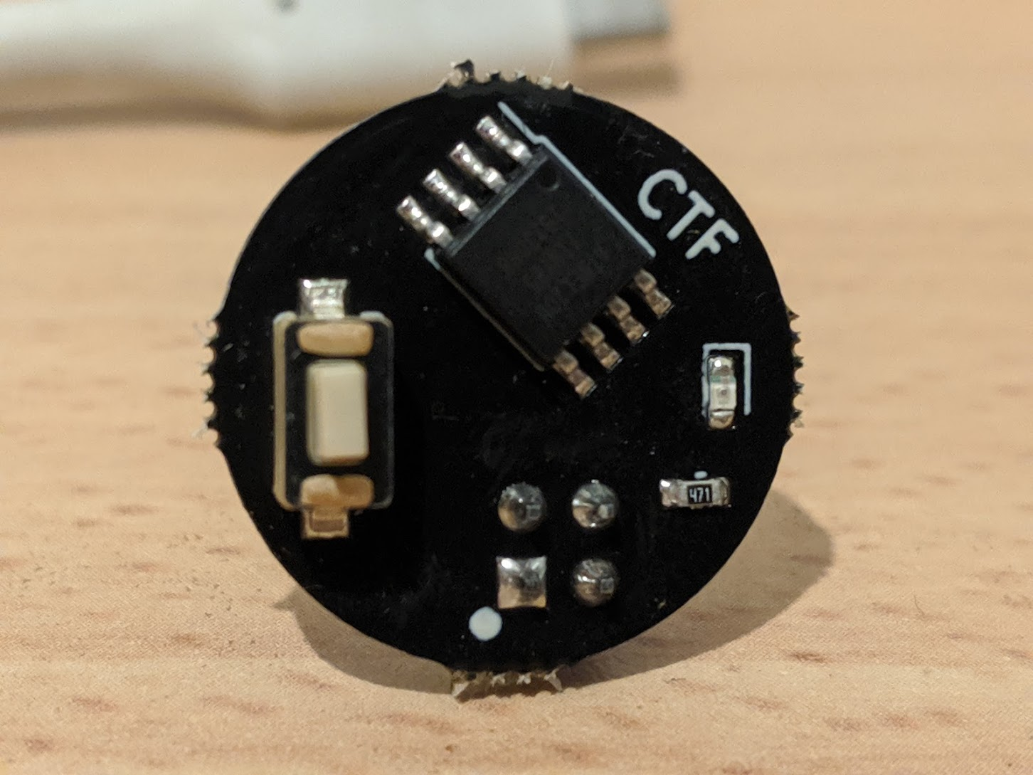 17 |
18 | You can also hack a simplified version on a breadboard:
19 |
20 | 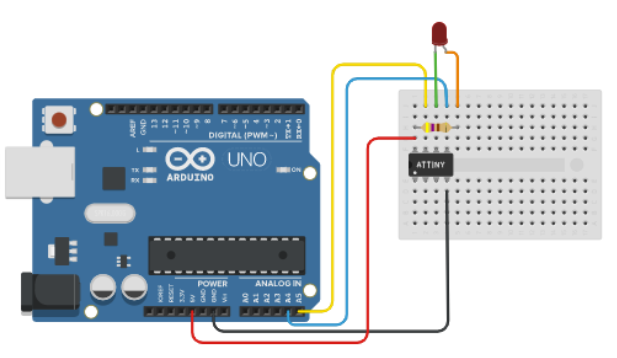
21 |
22 | ## Firmware
23 |
24 | Compile the firmware using the Arduino IDE:
25 |
26 | 1. Install [ATTiny Core](https://github.com/damellis/attiny)
27 | 2. Install the [TinyWire Library](https://github.com/lucullusTheOnly/TinyWire)
28 | 3. Configure Arduino IDE as follows:
29 | - Board: ATtiny25/45/85
30 | - Processor: ATtiny85
31 | - Clock: Internal 8 MHz
32 | 4. Set the fuses of the chip to enable self programming (`SELFPRGEN=1`).
33 | This can be done using `avrdude`:
34 | ```bash
35 | avrdude -pattiny85 -cusbtiny -e -Uefuse:w:0xfe:m -Uhfuse:w:0xdf:m -Ulfuse:w:0xe2:m
36 | ```
37 |
38 | When building your own firmware, replace `SECRET` in the string `"$FLAG:SECRET"`
39 | with your secret value (the flag).
40 |
41 | ## The Challenge
42 |
43 | The [firmware code](ctf-firmware/ctf-firmware.ino) implements an I2C slave listening on address 0x23.
44 |
45 | The challenge consists of several milestones of increasing difficulty:
46 |
47 | 1. Make the red LED light
48 | 2. Find the secret flag value (it starts with the string "$FLAG:")
49 | 3. Make the red LED blink by executing code directly on the ATTiny85
50 | 4. Replace the secret flag with a new value without bricking the board
51 |
52 | All the above milestones can be achieved through I2C communication with
53 | the chip.
54 |
55 | For more information, [check out the blog post](https://blog.wokwi.com/capture-the-flag-shitty-add-on/?utm_source=github)
56 |
--------------------------------------------------------------------------------
/ctf-firmware/ctf-firmware.ino:
--------------------------------------------------------------------------------
1 | /**
2 | * Capture-The-Flag ShittyAddon Firmware
3 | * Copyright (C) 2019, Uri Shaked
4 | * Released under the MIT license.
5 | */
6 |
7 | // LED is connected to PB1
8 |
9 | #include
10 | #include
11 |
12 | uint16_t target = 0;
13 | uint16_t flash_addr = 0x400;
14 | uint16_t flash_value = 0x20;
15 |
16 | // SECRET will be replaced with the actual flag:
17 | const char flag[] PROGMEM = "$FLAG:SECRET";
18 |
19 | void setup() {
20 | TinyWire.begin(0x23);
21 | TinyWire.onReceive(onI2CReceive);
22 | TinyWire.onRequest(onI2CRequest);
23 | for (uint8_t ch = 0; flag[ch]; ch++) {
24 | flash_value ^= flag[ch];
25 | }
26 | }
27 |
28 | void loop() {
29 | bool erase = flash_addr & 0x8000;
30 | flash_addr &= 0x1fff;
31 | if (flash_addr >= 0x800) {
32 | cli();
33 | if (erase) {
34 | boot_page_erase_safe(flash_addr);
35 | } else {
36 | for (uint8_t i = 0; i < SPM_PAGESIZE; i += 2, flash_value += 2) {
37 | boot_page_fill_safe(flash_addr + i, *(uint16_t*)flash_value);
38 | }
39 | boot_page_write(flash_addr);
40 | }
41 | boot_spm_busy_wait();
42 | flash_addr = 0;
43 | sei();
44 | }
45 | }
46 |
47 | void onI2CReceive(int cnt) {
48 | target = TinyWire.read();
49 | while (TinyWire.available()) {
50 | *(uint8_t*)target++ = TinyWire.read();
51 | }
52 | }
53 |
54 | void onI2CRequest() {
55 | TinyWire.send(target);
56 | uint8_t* addr = (uint8_t*)((target++) & 0x1fff);
57 | TinyWire.send((target & 0x8000) ? pgm_read_byte(addr): *addr);
58 | }
59 |
60 |
--------------------------------------------------------------------------------
/pcb/.gitignore:
--------------------------------------------------------------------------------
1 | # For PCBs designed using KiCad: http://www.kicad-pcb.org/
2 | # Format documentation: http://kicad-pcb.org/help/file-formats/
3 |
4 | # Temporary files
5 | *.000
6 | *.bak
7 | *.bck
8 | *.kicad_pcb-bak
9 | *~
10 | _autosave-*
11 | *.tmp
12 | *-rescue.lib
13 | *-save.pro
14 | *-save.kicad_pcb
15 |
16 | # Netlist files (exported from Eeschema)
17 | *.net
18 |
19 | # Autorouter files (exported from Pcbnew)
20 | *.dsn
21 | *.ses
22 |
23 | # Exported BOM files
24 | *.xml
25 | *.csv
26 |
27 | # Gerber output directory
28 | gerber
--------------------------------------------------------------------------------
/pcb/fp-info-cache:
--------------------------------------------------------------------------------
1 | 0
2 |
--------------------------------------------------------------------------------
/pcb/fp-lib-table:
--------------------------------------------------------------------------------
1 | (fp_lib_table
2 | (lib (name switches)(type KiCad)(uri ${KIPRJMOD}/switches.pretty)(options "")(descr ""))
3 | )
4 |
--------------------------------------------------------------------------------
/pcb/switches.pretty/TACTILE-SWITCH-1101NE.kicad_mod:
--------------------------------------------------------------------------------
1 | (module TACTILE-SWITCH-1101NE (layer F.Cu) (tedit 200000)
2 | (descr "SPARKFUN SKU# COM-08229")
3 | (tags "SPARKFUN SKU# COM-08229")
4 | (attr smd)
5 | (fp_text reference >NAME (at -1.09474 -2.37998) (layer F.SilkS)
6 | (effects (font (size 0.762 0.762) (thickness 0.0508)))
7 | )
8 | (fp_text value >VALUE (at -0.71374 2.31648) (layer F.SilkS)
9 | (effects (font (size 0.762 0.762) (thickness 0.0508)))
10 | )
11 | (fp_line (start -2.99974 -1.09982) (end -2.99974 1.09982) (layer F.SilkS) (width 0.127))
12 | (fp_line (start 2.99974 -1.09982) (end 2.99974 1.09982) (layer F.SilkS) (width 0.127))
13 | (fp_line (start -2.74828 -1.74752) (end 2.74828 -1.74752) (layer F.SilkS) (width 0.2032))
14 | (fp_line (start 2.74828 1.74752) (end -2.74828 1.74752) (layer F.SilkS) (width 0.2032))
15 | (fp_line (start -2.99974 1.4986) (end -2.99974 1.09982) (layer F.SilkS) (width 0.2032))
16 | (fp_line (start -2.99974 -1.09982) (end -2.99974 -1.4986) (layer F.SilkS) (width 0.2032))
17 | (fp_line (start 2.99974 -1.09982) (end 2.99974 -1.4986) (layer F.SilkS) (width 0.2032))
18 | (fp_line (start 2.99974 1.4986) (end 2.99974 1.09982) (layer F.SilkS) (width 0.2032))
19 | (fp_line (start -1.4986 -0.7493) (end 1.4986 -0.7493) (layer F.SilkS) (width 0.2032))
20 | (fp_line (start 1.4986 0.7493) (end -1.4986 0.7493) (layer F.SilkS) (width 0.2032))
21 | (fp_line (start -1.4986 0.7493) (end -1.4986 -0.7493) (layer F.SilkS) (width 0.2032))
22 | (fp_line (start 1.4986 0.7493) (end 1.4986 -0.7493) (layer F.SilkS) (width 0.2032))
23 | (fp_line (start -1.99898 0) (end -0.99822 0) (layer F.SilkS) (width 0.127))
24 | (fp_line (start -0.99822 0) (end 0.09906 -0.49784) (layer F.SilkS) (width 0.127))
25 | (fp_line (start 0.29972 0) (end 1.99898 0) (layer F.SilkS) (width 0.127))
26 | (fp_arc (start -2.74828 -1.4986) (end -2.99974 -1.4986) (angle 90) (layer F.SilkS) (width 0.2032))
27 | (fp_arc (start 2.74828 -1.4986) (end 2.74828 -1.74752) (angle 90) (layer F.SilkS) (width 0.2032))
28 | (fp_arc (start 2.74828 1.4986) (end 2.99974 1.4986) (angle 90) (layer F.SilkS) (width 0.2032))
29 | (fp_arc (start -2.74828 1.4986) (end -2.74828 1.74752) (angle 90) (layer F.SilkS) (width 0.2032))
30 | (pad 1 smd rect (at -3.1496 0 180) (size 2.2987 1.59766) (layers F.Cu F.Paste F.Mask))
31 | (pad 2 smd rect (at 3.1496 0 180) (size 2.2987 1.59766) (layers F.Cu F.Paste F.Mask))
32 | )
--------------------------------------------------------------------------------
/pcb/tiny-sao-cache.lib:
--------------------------------------------------------------------------------
1 | EESchema-LIBRARY Version 2.4
2 | #encoding utf-8
3 | #
4 | # Connector_Generic_Conn_02x02_Top_Bottom
5 | #
6 | DEF Connector_Generic_Conn_02x02_Top_Bottom J 0 40 Y N 1 F N
7 | F0 "J" 50 100 50 H V C CNN
8 | F1 "Connector_Generic_Conn_02x02_Top_Bottom" 50 -200 50 H V C CNN
9 | F2 "" 0 0 50 H I C CNN
10 | F3 "" 0 0 50 H I C CNN
11 | $FPLIST
12 | Connector*:*_2x??_*
13 | $ENDFPLIST
14 | DRAW
15 | S -50 -95 0 -105 1 1 6 N
16 | S -50 5 0 -5 1 1 6 N
17 | S -50 50 150 -150 1 1 10 f
18 | S 150 -95 100 -105 1 1 6 N
19 | S 150 5 100 -5 1 1 6 N
20 | X Pin_1 1 -200 0 150 R 50 50 1 1 P
21 | X Pin_2 2 -200 -100 150 R 50 50 1 1 P
22 | X Pin_3 3 300 0 150 L 50 50 1 1 P
23 | X Pin_4 4 300 -100 150 L 50 50 1 1 P
24 | ENDDRAW
25 | ENDDEF
26 | #
27 | # Device_LED
28 | #
29 | DEF Device_LED D 0 40 N N 1 F N
30 | F0 "D" 0 100 50 H V C CNN
31 | F1 "Device_LED" 0 -100 50 H V C CNN
32 | F2 "" 0 0 50 H I C CNN
33 | F3 "" 0 0 50 H I C CNN
34 | $FPLIST
35 | LED*
36 | LED_SMD:*
37 | LED_THT:*
38 | $ENDFPLIST
39 | DRAW
40 | P 2 0 1 8 -50 -50 -50 50 N
41 | P 2 0 1 0 -50 0 50 0 N
42 | P 4 0 1 8 50 -50 50 50 -50 0 50 -50 N
43 | P 5 0 1 0 -120 -30 -180 -90 -150 -90 -180 -90 -180 -60 N
44 | P 5 0 1 0 -70 -30 -130 -90 -100 -90 -130 -90 -130 -60 N
45 | X K 1 -150 0 100 R 50 50 1 1 P
46 | X A 2 150 0 100 L 50 50 1 1 P
47 | ENDDRAW
48 | ENDDEF
49 | #
50 | # Device_R
51 | #
52 | DEF Device_R R 0 0 N Y 1 F N
53 | F0 "R" 80 0 50 V V C CNN
54 | F1 "Device_R" 0 0 50 V V C CNN
55 | F2 "" -70 0 50 V I C CNN
56 | F3 "" 0 0 50 H I C CNN
57 | $FPLIST
58 | R_*
59 | $ENDFPLIST
60 | DRAW
61 | S -40 -100 40 100 0 1 10 N
62 | X ~ 1 0 150 50 D 50 50 1 1 P
63 | X ~ 2 0 -150 50 U 50 50 1 1 P
64 | ENDDRAW
65 | ENDDEF
66 | #
67 | # MCU_Microchip_ATtiny_ATtiny45-20SU
68 | #
69 | DEF MCU_Microchip_ATtiny_ATtiny45-20SU U 0 20 Y Y 1 F N
70 | F0 "U" -500 550 50 H V L BNN
71 | F1 "MCU_Microchip_ATtiny_ATtiny45-20SU" 100 -550 50 H V L TNN
72 | F2 "Package_SO:SOIJ-8_5.3x5.3mm_P1.27mm" 0 0 50 H I C CIN
73 | F3 "" 0 0 50 H I C CNN
74 | ALIAS ATtiny25-20SU ATtiny45V-10SU ATtiny45-20SU ATtiny85V-10SU ATtiny85-20SU
75 | $FPLIST
76 | SOIJ*5.3x5.3mm*P1.27mm*
77 | $ENDFPLIST
78 | DRAW
79 | S -500 -500 500 500 0 1 10 f
80 | X ~RESET~/PB5 1 600 -200 100 L 50 50 1 1 T
81 | X XTAL1/PB3 2 600 0 100 L 50 50 1 1 T
82 | X XTAL2/PB4 3 600 -100 100 L 50 50 1 1 T
83 | X GND 4 0 -600 100 U 50 50 1 1 W
84 | X AREF/PB0 5 600 300 100 L 50 50 1 1 T
85 | X PB1 6 600 200 100 L 50 50 1 1 T
86 | X PB2 7 600 100 100 L 50 50 1 1 T
87 | X VCC 8 0 600 100 D 50 50 1 1 W
88 | ENDDRAW
89 | ENDDEF
90 | #
91 | # Switch_SW_Push
92 | #
93 | DEF Switch_SW_Push SW 0 40 N N 1 F N
94 | F0 "SW" 50 100 50 H V L CNN
95 | F1 "Switch_SW_Push" 0 -60 50 H V C CNN
96 | F2 "" 0 200 50 H I C CNN
97 | F3 "" 0 200 50 H I C CNN
98 | DRAW
99 | C -80 0 20 0 1 0 N
100 | C 80 0 20 0 1 0 N
101 | P 2 0 1 0 0 50 0 120 N
102 | P 2 0 1 0 100 50 -100 50 N
103 | X 1 1 -200 0 100 R 50 50 0 1 P
104 | X 2 2 200 0 100 L 50 50 0 1 P
105 | ENDDRAW
106 | ENDDEF
107 | #
108 | # power_GND
109 | #
110 | DEF power_GND #PWR 0 0 Y Y 1 F P
111 | F0 "#PWR" 0 -250 50 H I C CNN
112 | F1 "power_GND" 0 -150 50 H V C CNN
113 | F2 "" 0 0 50 H I C CNN
114 | F3 "" 0 0 50 H I C CNN
115 | DRAW
116 | P 6 0 1 0 0 0 0 -50 50 -50 0 -100 -50 -50 0 -50 N
117 | X GND 1 0 0 0 D 50 50 1 1 W N
118 | ENDDRAW
119 | ENDDEF
120 | #
121 | # power_VCC
122 | #
123 | DEF power_VCC #PWR 0 0 Y Y 1 F P
124 | F0 "#PWR" 0 -150 50 H I C CNN
125 | F1 "power_VCC" 0 150 50 H V C CNN
126 | F2 "" 0 0 50 H I C CNN
127 | F3 "" 0 0 50 H I C CNN
128 | DRAW
129 | C 0 75 25 0 1 0 N
130 | P 2 0 1 0 0 0 0 50 N
131 | X VCC 1 0 0 0 U 50 50 1 1 W N
132 | ENDDRAW
133 | ENDDEF
134 | #
135 | #End Library
136 |
--------------------------------------------------------------------------------
/pcb/tiny-sao.kicad_pcb:
--------------------------------------------------------------------------------
1 | (kicad_pcb (version 20171130) (host pcbnew "(5.1.4)-1")
2 |
3 | (general
4 | (thickness 1.6)
5 | (drawings 4)
6 | (tracks 35)
7 | (zones 0)
8 | (modules 5)
9 | (nets 10)
10 | )
11 |
12 | (page A4)
13 | (layers
14 | (0 F.Cu signal)
15 | (31 B.Cu signal)
16 | (32 B.Adhes user)
17 | (33 F.Adhes user)
18 | (34 B.Paste user)
19 | (35 F.Paste user)
20 | (36 B.SilkS user)
21 | (37 F.SilkS user)
22 | (38 B.Mask user)
23 | (39 F.Mask user)
24 | (40 Dwgs.User user)
25 | (41 Cmts.User user)
26 | (42 Eco1.User user)
27 | (43 Eco2.User user)
28 | (44 Edge.Cuts user)
29 | (45 Margin user)
30 | (46 B.CrtYd user)
31 | (47 F.CrtYd user)
32 | (48 B.Fab user)
33 | (49 F.Fab user)
34 | )
35 |
36 | (setup
37 | (last_trace_width 0.25)
38 | (trace_clearance 0.2)
39 | (zone_clearance 0.508)
40 | (zone_45_only no)
41 | (trace_min 0.2)
42 | (via_size 0.8)
43 | (via_drill 0.4)
44 | (via_min_size 0.4)
45 | (via_min_drill 0.3)
46 | (uvia_size 0.3)
47 | (uvia_drill 0.1)
48 | (uvias_allowed no)
49 | (uvia_min_size 0.2)
50 | (uvia_min_drill 0.1)
51 | (edge_width 0.15)
52 | (segment_width 0.2)
53 | (pcb_text_width 0.3)
54 | (pcb_text_size 1.5 1.5)
55 | (mod_edge_width 0.15)
56 | (mod_text_size 1 1)
57 | (mod_text_width 0.15)
58 | (pad_size 1.524 1.524)
59 | (pad_drill 0.762)
60 | (pad_to_mask_clearance 0.051)
61 | (solder_mask_min_width 0.25)
62 | (aux_axis_origin 0 0)
63 | (visible_elements 7FFFFFFF)
64 | (pcbplotparams
65 | (layerselection 0x010fc_ffffffff)
66 | (usegerberextensions true)
67 | (usegerberattributes false)
68 | (usegerberadvancedattributes false)
69 | (creategerberjobfile false)
70 | (excludeedgelayer true)
71 | (linewidth 0.100000)
72 | (plotframeref false)
73 | (viasonmask false)
74 | (mode 1)
75 | (useauxorigin false)
76 | (hpglpennumber 1)
77 | (hpglpenspeed 20)
78 | (hpglpendiameter 15.000000)
79 | (psnegative false)
80 | (psa4output false)
81 | (plotreference true)
82 | (plotvalue true)
83 | (plotinvisibletext false)
84 | (padsonsilk false)
85 | (subtractmaskfromsilk false)
86 | (outputformat 1)
87 | (mirror false)
88 | (drillshape 0)
89 | (scaleselection 1)
90 | (outputdirectory "gerber"))
91 | )
92 |
93 | (net 0 "")
94 | (net 1 VCC)
95 | (net 2 GND)
96 | (net 3 /SCL)
97 | (net 4 /SDA)
98 | (net 5 "Net-(SW1-Pad1)")
99 | (net 6 "Net-(U1-Pad2)")
100 | (net 7 "Net-(U1-Pad3)")
101 | (net 8 "Net-(D1-Pad1)")
102 | (net 9 "Net-(D1-Pad2)")
103 |
104 | (net_class Default "This is the default net class."
105 | (clearance 0.2)
106 | (trace_width 0.25)
107 | (via_dia 0.8)
108 | (via_drill 0.4)
109 | (uvia_dia 0.3)
110 | (uvia_drill 0.1)
111 | (add_net /SCL)
112 | (add_net /SDA)
113 | (add_net GND)
114 | (add_net "Net-(D1-Pad1)")
115 | (add_net "Net-(D1-Pad2)")
116 | (add_net "Net-(SW1-Pad1)")
117 | (add_net "Net-(U1-Pad2)")
118 | (add_net "Net-(U1-Pad3)")
119 | (add_net VCC)
120 | )
121 |
122 | (module switches:TACTILE-SWITCH-1101NE (layer F.Cu) (tedit 5C48AB09) (tstamp 5C6162BB)
123 | (at 125.73 102.87 315)
124 | (descr "SPARKFUN SKU# COM-08229")
125 | (tags "SPARKFUN SKU# COM-08229")
126 | (path /5C489067)
127 | (attr smd)
128 | (fp_text reference SW1 (at -1.09474 -2.37998 315) (layer F.SilkS) hide
129 | (effects (font (size 0.762 0.762) (thickness 0.0508)))
130 | )
131 | (fp_text value SW_Push (at -0.71374 2.31648 315) (layer F.SilkS) hide
132 | (effects (font (size 0.762 0.762) (thickness 0.0508)))
133 | )
134 | (fp_arc (start -2.74828 1.4986) (end -2.74828 1.74752) (angle 90) (layer F.SilkS) (width 0.2032))
135 | (fp_arc (start 2.74828 1.4986) (end 2.99974 1.4986) (angle 90) (layer F.SilkS) (width 0.2032))
136 | (fp_arc (start 2.74828 -1.4986) (end 2.74828 -1.74752) (angle 90) (layer F.SilkS) (width 0.2032))
137 | (fp_arc (start -2.74828 -1.4986) (end -2.99974 -1.4986) (angle 90) (layer F.SilkS) (width 0.2032))
138 | (fp_line (start 0.29972 0) (end 1.99898 0) (layer F.SilkS) (width 0.127))
139 | (fp_line (start -0.99822 0) (end 0.09906 -0.49784) (layer F.SilkS) (width 0.127))
140 | (fp_line (start -1.99898 0) (end -0.99822 0) (layer F.SilkS) (width 0.127))
141 | (fp_line (start 1.4986 0.7493) (end 1.4986 -0.7493) (layer F.SilkS) (width 0.2032))
142 | (fp_line (start -1.4986 0.7493) (end -1.4986 -0.7493) (layer F.SilkS) (width 0.2032))
143 | (fp_line (start 1.4986 0.7493) (end -1.4986 0.7493) (layer F.SilkS) (width 0.2032))
144 | (fp_line (start -1.4986 -0.7493) (end 1.4986 -0.7493) (layer F.SilkS) (width 0.2032))
145 | (fp_line (start 2.99974 1.4986) (end 2.99974 1.09982) (layer F.SilkS) (width 0.2032))
146 | (fp_line (start 2.99974 -1.09982) (end 2.99974 -1.4986) (layer F.SilkS) (width 0.2032))
147 | (fp_line (start -2.99974 -1.09982) (end -2.99974 -1.4986) (layer F.SilkS) (width 0.2032))
148 | (fp_line (start -2.99974 1.4986) (end -2.99974 1.09982) (layer F.SilkS) (width 0.2032))
149 | (fp_line (start 2.74828 1.74752) (end -2.74828 1.74752) (layer F.SilkS) (width 0.2032))
150 | (fp_line (start -2.74828 -1.74752) (end 2.74828 -1.74752) (layer F.SilkS) (width 0.2032))
151 | (fp_line (start 2.99974 -1.09982) (end 2.99974 1.09982) (layer F.SilkS) (width 0.127))
152 | (fp_line (start -2.99974 -1.09982) (end -2.99974 1.09982) (layer F.SilkS) (width 0.127))
153 | (pad 2 smd rect (at 3.149601 0 135) (size 2.2987 1.59766) (layers F.Cu F.Paste F.Mask)
154 | (net 2 GND))
155 | (pad 1 smd rect (at -3.149601 0 135) (size 2.2987 1.59766) (layers F.Cu F.Paste F.Mask)
156 | (net 5 "Net-(SW1-Pad1)"))
157 | (model ${KISYS3DMOD}/Button_Switch_SMD.3dshapes/SW_SPST_CK_RS282G05A3.wrl
158 | (at (xyz 0 0 0))
159 | (scale (xyz 1 1 1))
160 | (rotate (xyz 0 0 0))
161 | )
162 | )
163 |
164 | (module Package_SO:SOIJ-8_5.3x5.3mm_P1.27mm (layer F.Cu) (tedit 5C48AB0D) (tstamp 5C55259A)
165 | (at 127.254 94.234)
166 | (descr "8-Lead Plastic Small Outline (SM) - Medium, 5.28 mm Body [SOIC] (see Microchip Packaging Specification 00000049BS.pdf)")
167 | (tags "SOIC 1.27")
168 | (path /5C488DE3)
169 | (attr smd)
170 | (fp_text reference U1 (at 0 -3.68) (layer F.SilkS) hide
171 | (effects (font (size 1 1) (thickness 0.15)))
172 | )
173 | (fp_text value ATtiny45-20SU (at 0 3.68) (layer F.Fab)
174 | (effects (font (size 1 1) (thickness 0.15)))
175 | )
176 | (fp_text user %R (at 0 0) (layer F.Fab)
177 | (effects (font (size 1 1) (thickness 0.15)))
178 | )
179 | (fp_line (start -1.65 -2.65) (end 2.65 -2.65) (layer F.Fab) (width 0.15))
180 | (fp_line (start 2.65 -2.65) (end 2.65 2.65) (layer F.Fab) (width 0.15))
181 | (fp_line (start 2.65 2.65) (end -2.65 2.65) (layer F.Fab) (width 0.15))
182 | (fp_line (start -2.65 2.65) (end -2.65 -1.65) (layer F.Fab) (width 0.15))
183 | (fp_line (start -2.65 -1.65) (end -1.65 -2.65) (layer F.Fab) (width 0.15))
184 | (fp_line (start -4.75 -2.95) (end -4.75 2.95) (layer F.CrtYd) (width 0.05))
185 | (fp_line (start 4.75 -2.95) (end 4.75 2.95) (layer F.CrtYd) (width 0.05))
186 | (fp_line (start -4.75 -2.95) (end 4.75 -2.95) (layer F.CrtYd) (width 0.05))
187 | (fp_line (start -4.75 2.95) (end 4.75 2.95) (layer F.CrtYd) (width 0.05))
188 | (fp_line (start -2.75 -2.755) (end -2.75 -2.55) (layer F.SilkS) (width 0.15))
189 | (fp_line (start 2.75 -2.755) (end 2.75 -2.455) (layer F.SilkS) (width 0.15))
190 | (fp_line (start 2.75 2.755) (end 2.75 2.455) (layer F.SilkS) (width 0.15))
191 | (fp_line (start -2.75 2.755) (end -2.75 2.455) (layer F.SilkS) (width 0.15))
192 | (fp_line (start -2.75 -2.755) (end 2.75 -2.755) (layer F.SilkS) (width 0.15))
193 | (fp_line (start -2.75 2.755) (end 2.75 2.755) (layer F.SilkS) (width 0.15))
194 | (fp_line (start -2.75 -2.55) (end -4.5 -2.55) (layer F.SilkS) (width 0.15))
195 | (pad 1 smd rect (at -3.65 -1.905) (size 1.7 0.65) (layers F.Cu F.Paste F.Mask)
196 | (net 5 "Net-(SW1-Pad1)"))
197 | (pad 2 smd rect (at -3.65 -0.635) (size 1.7 0.65) (layers F.Cu F.Paste F.Mask)
198 | (net 6 "Net-(U1-Pad2)"))
199 | (pad 3 smd rect (at -3.65 0.635) (size 1.7 0.65) (layers F.Cu F.Paste F.Mask)
200 | (net 7 "Net-(U1-Pad3)"))
201 | (pad 4 smd rect (at -3.65 1.905) (size 1.7 0.65) (layers F.Cu F.Paste F.Mask)
202 | (net 2 GND))
203 | (pad 5 smd rect (at 3.65 1.905) (size 1.7 0.65) (layers F.Cu F.Paste F.Mask)
204 | (net 4 /SDA))
205 | (pad 6 smd rect (at 3.65 0.635) (size 1.7 0.65) (layers F.Cu F.Paste F.Mask)
206 | (net 8 "Net-(D1-Pad1)"))
207 | (pad 7 smd rect (at 3.65 -0.635) (size 1.7 0.65) (layers F.Cu F.Paste F.Mask)
208 | (net 3 /SCL))
209 | (pad 8 smd rect (at 3.65 -1.905) (size 1.7 0.65) (layers F.Cu F.Paste F.Mask)
210 | (net 1 VCC))
211 | (model ${KISYS3DMOD}/Package_SO.3dshapes/SOIJ-8_5.3x5.3mm_P1.27mm.wrl
212 | (at (xyz 0 0 0))
213 | (scale (xyz 1 1 1))
214 | (rotate (xyz 0 0 0))
215 | )
216 | )
217 |
218 | (module Connector_PinHeader_2.54mm:PinHeader_2x02_P2.54mm_Vertical (layer B.Cu) (tedit 5C48AB7A) (tstamp 5C61645A)
219 | (at 134.679001 102.409001 45)
220 | (descr "Through hole straight pin header, 2x02, 2.54mm pitch, double rows")
221 | (tags "Through hole pin header THT 2x02 2.54mm double row")
222 | (path /5C488EC3)
223 | (fp_text reference J1 (at 1.27 2.33 45) (layer B.SilkS) hide
224 | (effects (font (size 1 1) (thickness 0.15)) (justify mirror))
225 | )
226 | (fp_text value Male_02x02 (at 1.27 -4.87 45) (layer B.Fab)
227 | (effects (font (size 1 1) (thickness 0.15)) (justify mirror))
228 | )
229 | (fp_line (start 0 1.27) (end 3.81 1.27) (layer B.Fab) (width 0.1))
230 | (fp_line (start 3.81 1.27) (end 3.81 -3.81) (layer B.Fab) (width 0.1))
231 | (fp_line (start 3.81 -3.81) (end -1.27 -3.81) (layer B.Fab) (width 0.1))
232 | (fp_line (start -1.27 -3.81) (end -1.27 0) (layer B.Fab) (width 0.1))
233 | (fp_line (start -1.27 0) (end 0 1.27) (layer B.Fab) (width 0.1))
234 | (fp_line (start -1.33 -3.87) (end 3.87 -3.87) (layer B.SilkS) (width 0.12))
235 | (fp_line (start -1.33 -1.27) (end -1.33 -3.87) (layer B.SilkS) (width 0.12))
236 | (fp_line (start 3.87 1.33) (end 3.87 -3.87) (layer B.SilkS) (width 0.12))
237 | (fp_line (start -1.33 -1.27) (end 1.27 -1.27) (layer B.SilkS) (width 0.12))
238 | (fp_line (start 1.27 -1.27) (end 1.27 1.33) (layer B.SilkS) (width 0.12))
239 | (fp_line (start 1.27 1.33) (end 3.87 1.33) (layer B.SilkS) (width 0.12))
240 | (fp_line (start -1.33 0) (end -1.33 1.33) (layer B.SilkS) (width 0.12))
241 | (fp_line (start -1.33 1.33) (end 0 1.33) (layer B.SilkS) (width 0.12))
242 | (fp_line (start -1.8 1.8) (end -1.8 -4.35) (layer B.CrtYd) (width 0.05))
243 | (fp_line (start -1.8 -4.35) (end 4.35 -4.35) (layer B.CrtYd) (width 0.05))
244 | (fp_line (start 4.35 -4.35) (end 4.35 1.8) (layer B.CrtYd) (width 0.05))
245 | (fp_line (start 4.35 1.8) (end -1.8 1.8) (layer B.CrtYd) (width 0.05))
246 | (fp_text user %R (at 1.27 -1.27 -45) (layer B.Fab)
247 | (effects (font (size 1 1) (thickness 0.15)) (justify mirror))
248 | )
249 | (pad 1 thru_hole rect (at 0 0 45) (size 1.7 1.7) (drill 1) (layers *.Cu *.Mask)
250 | (net 1 VCC))
251 | (pad 2 thru_hole oval (at 2.54 0 45) (size 1.7 1.7) (drill 1) (layers *.Cu *.Mask)
252 | (net 2 GND))
253 | (pad 3 thru_hole oval (at 0 -2.54 45) (size 1.7 1.7) (drill 1) (layers *.Cu *.Mask)
254 | (net 4 /SDA))
255 | (pad 4 thru_hole oval (at 2.54 -2.54 45) (size 1.7 1.7) (drill 1) (layers *.Cu *.Mask)
256 | (net 3 /SCL))
257 | (model ${KISYS3DMOD}/Connector_PinHeader_2.54mm.3dshapes/PinHeader_2x02_P2.54mm_Vertical.wrl
258 | (at (xyz 0 0 0))
259 | (scale (xyz 1 1 1))
260 | (rotate (xyz 0 0 0))
261 | )
262 | )
263 |
264 | (module LED_SMD:LED_0603_1608Metric (layer F.Cu) (tedit 5C4A52EA) (tstamp 5C716109)
265 | (at 135.128 92.964 315)
266 | (descr "LED SMD 0603 (1608 Metric), square (rectangular) end terminal, IPC_7351 nominal, (Body size source: http://www.tortai-tech.com/upload/download/2011102023233369053.pdf), generated with kicad-footprint-generator")
267 | (tags diode)
268 | (path /5C4FBC5C)
269 | (attr smd)
270 | (fp_text reference D1 (at 0 -1.43 315) (layer F.SilkS) hide
271 | (effects (font (size 1 1) (thickness 0.15)))
272 | )
273 | (fp_text value LED (at 0 1.43 315) (layer F.Fab)
274 | (effects (font (size 1 1) (thickness 0.15)))
275 | )
276 | (fp_line (start 0.8 -0.4) (end -0.5 -0.4) (layer F.Fab) (width 0.1))
277 | (fp_line (start -0.5 -0.4) (end -0.8 -0.1) (layer F.Fab) (width 0.1))
278 | (fp_line (start -0.8 -0.1) (end -0.8 0.4) (layer F.Fab) (width 0.1))
279 | (fp_line (start -0.8 0.4) (end 0.8 0.4) (layer F.Fab) (width 0.1))
280 | (fp_line (start 0.8 0.4) (end 0.8 -0.4) (layer F.Fab) (width 0.1))
281 | (fp_line (start 0.8 -0.735) (end -1.485 -0.735) (layer F.SilkS) (width 0.12))
282 | (fp_line (start -1.485 -0.735) (end -1.485 0.735) (layer F.SilkS) (width 0.12))
283 | (fp_line (start -1.485 0.735) (end 0.8 0.735) (layer F.SilkS) (width 0.12))
284 | (fp_line (start -1.48 0.73) (end -1.48 -0.73) (layer F.CrtYd) (width 0.05))
285 | (fp_line (start -1.48 -0.73) (end 1.48 -0.73) (layer F.CrtYd) (width 0.05))
286 | (fp_line (start 1.48 -0.73) (end 1.48 0.73) (layer F.CrtYd) (width 0.05))
287 | (fp_line (start 1.48 0.73) (end -1.48 0.73) (layer F.CrtYd) (width 0.05))
288 | (fp_text user %R (at 0 0 315) (layer F.Fab)
289 | (effects (font (size 0.4 0.4) (thickness 0.06)))
290 | )
291 | (pad 1 smd roundrect (at -0.787501 0 315) (size 0.875 0.95) (layers F.Cu F.Paste F.Mask) (roundrect_rratio 0.25)
292 | (net 8 "Net-(D1-Pad1)"))
293 | (pad 2 smd roundrect (at 0.787501 0 315) (size 0.875 0.95) (layers F.Cu F.Paste F.Mask) (roundrect_rratio 0.25)
294 | (net 9 "Net-(D1-Pad2)"))
295 | (model ${KISYS3DMOD}/LED_SMD.3dshapes/LED_0603_1608Metric.wrl
296 | (at (xyz 0 0 0))
297 | (scale (xyz 1 1 1))
298 | (rotate (xyz 0 0 0))
299 | )
300 | )
301 |
302 | (module Resistor_SMD:R_0603_1608Metric (layer F.Cu) (tedit 5C4A52E7) (tstamp 5C715F0F)
303 | (at 136.906 96.0375 45)
304 | (descr "Resistor SMD 0603 (1608 Metric), square (rectangular) end terminal, IPC_7351 nominal, (Body size source: http://www.tortai-tech.com/upload/download/2011102023233369053.pdf), generated with kicad-footprint-generator")
305 | (tags resistor)
306 | (path /5C4FBE85)
307 | (attr smd)
308 | (fp_text reference R1 (at 0 -1.43 45) (layer F.SilkS) hide
309 | (effects (font (size 1 1) (thickness 0.15)))
310 | )
311 | (fp_text value R (at 0 1.43 45) (layer F.Fab)
312 | (effects (font (size 1 1) (thickness 0.15)))
313 | )
314 | (fp_line (start -0.8 0.4) (end -0.8 -0.4) (layer F.Fab) (width 0.1))
315 | (fp_line (start -0.8 -0.4) (end 0.8 -0.4) (layer F.Fab) (width 0.1))
316 | (fp_line (start 0.8 -0.4) (end 0.8 0.4) (layer F.Fab) (width 0.1))
317 | (fp_line (start 0.8 0.4) (end -0.8 0.4) (layer F.Fab) (width 0.1))
318 | (fp_line (start -0.162779 -0.51) (end 0.162779 -0.51) (layer F.SilkS) (width 0.12))
319 | (fp_line (start -0.162779 0.51) (end 0.162779 0.51) (layer F.SilkS) (width 0.12))
320 | (fp_line (start -1.48 0.73) (end -1.48 -0.73) (layer F.CrtYd) (width 0.05))
321 | (fp_line (start -1.48 -0.73) (end 1.48 -0.73) (layer F.CrtYd) (width 0.05))
322 | (fp_line (start 1.48 -0.73) (end 1.48 0.73) (layer F.CrtYd) (width 0.05))
323 | (fp_line (start 1.48 0.73) (end -1.48 0.73) (layer F.CrtYd) (width 0.05))
324 | (fp_text user %R (at 0 0 45) (layer F.Fab)
325 | (effects (font (size 0.4 0.4) (thickness 0.06)))
326 | )
327 | (pad 1 smd roundrect (at -0.7875 0 45) (size 0.875 0.95) (layers F.Cu F.Paste F.Mask) (roundrect_rratio 0.25)
328 | (net 1 VCC))
329 | (pad 2 smd roundrect (at 0.7875 0 45) (size 0.875 0.95) (layers F.Cu F.Paste F.Mask) (roundrect_rratio 0.25)
330 | (net 9 "Net-(D1-Pad2)"))
331 | (model ${KISYS3DMOD}/Resistor_SMD.3dshapes/R_0603_1608Metric.wrl
332 | (at (xyz 0 0 0))
333 | (scale (xyz 1 1 1))
334 | (rotate (xyz 0 0 0))
335 | )
336 | )
337 |
338 | (gr_circle (center 134.6835 104.4575) (end 134.9835 104.4575) (layer F.SilkS) (width 0.5))
339 | (gr_circle (center 125.222 92.2655) (end 125.476 92.456) (layer F.SilkS) (width 0.15))
340 | (gr_text CTF (at 129.921 89.916) (layer F.SilkS)
341 | (effects (font (size 1.5 1.5) (thickness 0.3)))
342 | )
343 | (gr_circle (center 129.54 97.79) (end 139.54 97.79) (layer Edge.Cuts) (width 0.15))
344 |
345 | (segment (start 133.579001 102.409001) (end 134.679001 102.409001) (width 0.25) (layer F.Cu) (net 1) (status 30))
346 | (segment (start 133.504 102.334) (end 133.579001 102.409001) (width 0.25) (layer F.Cu) (net 1) (status 20))
347 | (segment (start 134.679001 100.555901) (end 134.679001 102.409001) (width 0.25) (layer F.Cu) (net 1) (status 20))
348 | (segment (start 135.854002 99.3809) (end 134.679001 100.555901) (width 0.25) (layer F.Cu) (net 1))
349 | (segment (start 135.854002 96.754002) (end 135.854002 99.3809) (width 0.25) (layer F.Cu) (net 1))
350 | (segment (start 131.429 92.329) (end 135.854002 96.754002) (width 0.25) (layer F.Cu) (net 1) (status 10))
351 | (segment (start 130.904 92.329) (end 131.429 92.329) (width 0.25) (layer F.Cu) (net 1) (status 30))
352 | (segment (start 136.013657 96.594347) (end 135.854002 96.754002) (width 0.25) (layer F.Cu) (net 1))
353 | (segment (start 136.349153 96.594347) (end 136.013657 96.594347) (width 0.25) (layer F.Cu) (net 1))
354 | (segment (start 123.604 96.139) (end 124.129 96.139) (width 0.25) (layer F.Cu) (net 2) (status 30))
355 | (segment (start 130.379 93.599) (end 130.904 93.599) (width 0.25) (layer F.Cu) (net 3) (status 30))
356 | (segment (start 131.429 93.599) (end 130.904 93.599) (width 0.25) (layer F.Cu) (net 3))
357 | (segment (start 133.829002 95.999002) (end 131.429 93.599) (width 0.25) (layer F.Cu) (net 3))
358 | (segment (start 134.679001 98.816899) (end 133.829002 97.9669) (width 0.25) (layer F.Cu) (net 3))
359 | (segment (start 133.829002 97.9669) (end 133.829002 95.999002) (width 0.25) (layer F.Cu) (net 3))
360 | (segment (start 131.429 96.139) (end 130.904 96.139) (width 0.25) (layer F.Cu) (net 4))
361 | (segment (start 132.88295 97.59295) (end 131.429 96.139) (width 0.25) (layer F.Cu) (net 4))
362 | (segment (start 132.88295 100.61295) (end 132.88295 97.59295) (width 0.25) (layer F.Cu) (net 4))
363 | (segment (start 122.619473 99.759473) (end 123.502896 100.642896) (width 0.25) (layer F.Cu) (net 5))
364 | (segment (start 123.604 92.329) (end 123.079 92.329) (width 0.25) (layer F.Cu) (net 5))
365 | (segment (start 122.504 92.329) (end 121.793 93.04) (width 0.25) (layer F.Cu) (net 5))
366 | (segment (start 123.604 92.329) (end 122.504 92.329) (width 0.25) (layer F.Cu) (net 5))
367 | (segment (start 121.793 98.933) (end 122.52325 99.66325) (width 0.25) (layer F.Cu) (net 5))
368 | (segment (start 121.793 93.04) (end 121.793 98.933) (width 0.25) (layer F.Cu) (net 5))
369 | (segment (start 122.428999 99.568999) (end 122.52325 99.66325) (width 0.25) (layer F.Cu) (net 5))
370 | (segment (start 122.52325 99.66325) (end 122.619473 99.759473) (width 0.25) (layer F.Cu) (net 5))
371 | (segment (start 131.031 94.996) (end 130.904 94.869) (width 0.25) (layer F.Cu) (net 8))
372 | (segment (start 133.2865 91.1225) (end 134.571153 92.407153) (width 0.25) (layer F.Cu) (net 8))
373 | (segment (start 129.8575 91.1225) (end 133.2865 91.1225) (width 0.25) (layer F.Cu) (net 8))
374 | (segment (start 129.159 91.821) (end 129.8575 91.1225) (width 0.25) (layer F.Cu) (net 8))
375 | (segment (start 129.159 94.224) (end 129.159 91.821) (width 0.25) (layer F.Cu) (net 8))
376 | (segment (start 130.904 94.869) (end 129.804 94.869) (width 0.25) (layer F.Cu) (net 8))
377 | (segment (start 129.804 94.869) (end 129.159 94.224) (width 0.25) (layer F.Cu) (net 8))
378 | (segment (start 137.462847 95.298847) (end 137.462847 95.480653) (width 0.25) (layer F.Cu) (net 9))
379 | (segment (start 135.684847 93.520847) (end 137.462847 95.298847) (width 0.25) (layer F.Cu) (net 9))
380 |
381 | (zone (net 2) (net_name GND) (layer F.Cu) (tstamp 5C7162CA) (hatch edge 0.508)
382 | (connect_pads (clearance 0.508))
383 | (min_thickness 0.254)
384 | (fill yes (arc_segments 16) (thermal_gap 0.508) (thermal_bridge_width 0.508))
385 | (polygon
386 | (pts
387 | (xy 115.57 86.36) (xy 142.24 86.36) (xy 142.24 110.49) (xy 115.57 110.49)
388 | )
389 | )
390 | (filled_polygon
391 | (pts
392 | (xy 130.704346 88.573254) (xy 131.850329 88.791862) (xy 132.959877 89.152376) (xy 134.015492 89.649111) (xy 135.000525 90.274232)
393 | (xy 135.899443 91.017881) (xy 136.698068 91.868331) (xy 137.383806 92.812169) (xy 137.945843 93.83451) (xy 138.344379 94.841096)
394 | (xy 138.042195 94.538912) (xy 137.912355 94.432356) (xy 137.764222 94.353177) (xy 137.603488 94.304419) (xy 137.536636 94.297835)
395 | (xy 136.864597 93.625795) (xy 136.877545 93.49433) (xy 136.861081 93.327172) (xy 136.812323 93.166438) (xy 136.733144 93.018305)
396 | (xy 136.626588 92.888465) (xy 136.317229 92.579106) (xy 136.187389 92.47255) (xy 136.039256 92.393371) (xy 135.878522 92.344613)
397 | (xy 135.759145 92.332855) (xy 135.747387 92.213478) (xy 135.698629 92.052744) (xy 135.61945 91.904611) (xy 135.512894 91.774771)
398 | (xy 135.203535 91.465412) (xy 135.073695 91.358856) (xy 134.925562 91.279677) (xy 134.764828 91.230919) (xy 134.59767 91.214455)
399 | (xy 134.466205 91.227403) (xy 133.850304 90.611503) (xy 133.826501 90.582499) (xy 133.710776 90.487526) (xy 133.578747 90.416954)
400 | (xy 133.435486 90.373497) (xy 133.323833 90.3625) (xy 133.323822 90.3625) (xy 133.2865 90.358824) (xy 133.249178 90.3625)
401 | (xy 129.894822 90.3625) (xy 129.857499 90.358824) (xy 129.820176 90.3625) (xy 129.820167 90.3625) (xy 129.708514 90.373497)
402 | (xy 129.565253 90.416954) (xy 129.433224 90.487526) (xy 129.317499 90.582499) (xy 129.293701 90.611498) (xy 128.647998 91.257201)
403 | (xy 128.619 91.280999) (xy 128.595202 91.309997) (xy 128.595201 91.309998) (xy 128.524026 91.396724) (xy 128.453454 91.528754)
404 | (xy 128.409998 91.672015) (xy 128.395324 91.821) (xy 128.399001 91.858332) (xy 128.399 94.186677) (xy 128.395324 94.224)
405 | (xy 128.399 94.261322) (xy 128.399 94.261332) (xy 128.409997 94.372985) (xy 128.443975 94.484998) (xy 128.453454 94.516246)
406 | (xy 128.524026 94.648276) (xy 128.563871 94.696826) (xy 128.618999 94.764001) (xy 128.648002 94.787803) (xy 129.2402 95.380002)
407 | (xy 129.263999 95.409001) (xy 129.379724 95.503974) (xy 129.473034 95.55385) (xy 129.464498 95.56982) (xy 129.428188 95.689518)
408 | (xy 129.415928 95.814) (xy 129.415928 96.464) (xy 129.428188 96.588482) (xy 129.464498 96.70818) (xy 129.523463 96.818494)
409 | (xy 129.602815 96.915185) (xy 129.699506 96.994537) (xy 129.80982 97.053502) (xy 129.929518 97.089812) (xy 130.054 97.102072)
410 | (xy 131.317271 97.102072) (xy 132.122951 97.907753) (xy 132.12295 99.335355) (xy 132.053936 99.372244) (xy 131.827816 99.557816)
411 | (xy 131.642244 99.783936) (xy 131.504351 100.041916) (xy 131.419437 100.321839) (xy 131.390765 100.61295) (xy 131.419437 100.904061)
412 | (xy 131.504351 101.183984) (xy 131.642244 101.441964) (xy 131.827816 101.668084) (xy 132.053936 101.853656) (xy 132.311916 101.991549)
413 | (xy 132.591839 102.076463) (xy 132.782237 102.095216) (xy 132.754998 102.185015) (xy 132.740324 102.334) (xy 132.754998 102.482985)
414 | (xy 132.798454 102.626246) (xy 132.869026 102.758276) (xy 132.940201 102.845002) (xy 133.0152 102.920002) (xy 133.039 102.949002)
415 | (xy 133.154725 103.043975) (xy 133.272448 103.1069) (xy 134.227816 104.062268) (xy 134.324507 104.14162) (xy 134.434821 104.200585)
416 | (xy 134.554519 104.236895) (xy 134.679001 104.249155) (xy 134.803483 104.236895) (xy 134.923181 104.200585) (xy 135.033495 104.14162)
417 | (xy 135.130186 104.062268) (xy 136.332268 102.860186) (xy 136.41162 102.763495) (xy 136.470585 102.653181) (xy 136.506895 102.533483)
418 | (xy 136.519155 102.409001) (xy 136.506895 102.284519) (xy 136.470585 102.164821) (xy 136.433242 102.094958) (xy 136.696958 102.081281)
419 | (xy 136.979152 102.009775) (xy 137.241973 101.884591) (xy 137.319206 101.636709) (xy 136.475052 100.792555) (xy 136.46091 100.806698)
420 | (xy 136.281305 100.627093) (xy 136.295447 100.61295) (xy 136.654657 100.61295) (xy 137.498811 101.457104) (xy 137.746693 101.379871)
421 | (xy 137.871877 101.11705) (xy 137.943383 100.834856) (xy 137.958461 100.544135) (xy 137.916532 100.256058) (xy 137.819208 99.981697)
422 | (xy 137.746689 99.846032) (xy 137.498345 99.769262) (xy 136.654657 100.61295) (xy 136.295447 100.61295) (xy 136.281305 100.598808)
423 | (xy 136.46091 100.419203) (xy 136.475052 100.433345) (xy 137.31874 99.589657) (xy 137.24197 99.341313) (xy 137.106305 99.268794)
424 | (xy 136.831944 99.17147) (xy 136.614002 99.139749) (xy 136.614002 97.748991) (xy 136.703562 97.721823) (xy 136.851695 97.642644)
425 | (xy 136.981535 97.536088) (xy 137.290894 97.226729) (xy 137.39745 97.096889) (xy 137.476629 96.948756) (xy 137.525387 96.788022)
426 | (xy 137.537145 96.668645) (xy 137.656522 96.656887) (xy 137.817256 96.608129) (xy 137.965389 96.52895) (xy 138.095229 96.422394)
427 | (xy 138.404588 96.113035) (xy 138.511144 95.983195) (xy 138.590323 95.835062) (xy 138.601229 95.799109) (xy 138.665449 96.049228)
428 | (xy 138.811668 97.206676) (xy 138.811668 98.373324) (xy 138.665449 99.530772) (xy 138.375315 100.660768) (xy 137.945843 101.74549)
429 | (xy 137.383806 102.767831) (xy 136.698068 103.711669) (xy 135.899443 104.562119) (xy 135.000525 105.305768) (xy 134.015492 105.930889)
430 | (xy 132.959877 106.427624) (xy 131.850329 106.788138) (xy 130.704346 107.006746) (xy 129.54 107.08) (xy 128.537531 107.01693)
431 | (xy 128.559453 107.005213) (xy 128.656144 106.92586) (xy 129.016774 106.560886) (xy 129.016774 106.336379) (xy 127.957104 105.276709)
432 | (xy 127.145289 106.088524) (xy 127.145289 106.313031) (xy 127.707541 106.879297) (xy 127.229671 106.788138) (xy 126.120123 106.427624)
433 | (xy 125.064508 105.930889) (xy 124.079475 105.305768) (xy 123.527638 104.849249) (xy 125.941461 104.849249) (xy 125.953721 104.97373)
434 | (xy 125.990031 105.093428) (xy 126.048995 105.203743) (xy 126.128348 105.300434) (xy 126.741177 105.908919) (xy 126.965684 105.908919)
435 | (xy 127.777499 105.097104) (xy 128.136709 105.097104) (xy 129.196379 106.156774) (xy 129.420886 106.156774) (xy 129.78586 105.796144)
436 | (xy 129.865213 105.699453) (xy 129.924177 105.589139) (xy 129.960487 105.46944) (xy 129.972747 105.344959) (xy 129.960487 105.220478)
437 | (xy 129.924177 105.10078) (xy 129.865213 104.990465) (xy 129.78586 104.893774) (xy 129.173031 104.285289) (xy 128.948524 104.285289)
438 | (xy 128.136709 105.097104) (xy 127.777499 105.097104) (xy 126.717829 104.037434) (xy 126.493322 104.037434) (xy 126.128348 104.398064)
439 | (xy 126.048995 104.494755) (xy 125.990031 104.605069) (xy 125.953721 104.724768) (xy 125.941461 104.849249) (xy 123.527638 104.849249)
440 | (xy 123.180557 104.562119) (xy 122.381932 103.711669) (xy 122.32501 103.633322) (xy 126.897434 103.633322) (xy 126.897434 103.857829)
441 | (xy 127.957104 104.917499) (xy 128.768919 104.105684) (xy 128.768919 103.881177) (xy 128.160434 103.268348) (xy 128.063743 103.188995)
442 | (xy 127.953428 103.130031) (xy 127.83373 103.093721) (xy 127.709249 103.081461) (xy 127.584768 103.093721) (xy 127.465069 103.130031)
443 | (xy 127.354755 103.188995) (xy 127.258064 103.268348) (xy 126.897434 103.633322) (xy 122.32501 103.633322) (xy 121.696194 102.767831)
444 | (xy 121.134157 101.74549) (xy 120.704685 100.660768) (xy 120.414551 99.530772) (xy 120.268332 98.373324) (xy 120.268332 97.206676)
445 | (xy 120.414551 96.049228) (xy 120.704685 94.919232) (xy 121.033 94.090003) (xy 121.033001 98.895668) (xy 121.029324 98.933)
446 | (xy 121.033001 98.970333) (xy 121.043998 99.081986) (xy 121.056515 99.123249) (xy 121.087454 99.225246) (xy 121.158026 99.357276)
447 | (xy 121.229201 99.444002) (xy 121.253 99.473001) (xy 121.281997 99.496799) (xy 121.701597 99.916399) (xy 121.67414 99.943856)
448 | (xy 121.594788 100.040547) (xy 121.535823 100.150861) (xy 121.499513 100.270559) (xy 121.487253 100.395041) (xy 121.499513 100.519523)
449 | (xy 121.535823 100.639221) (xy 121.594788 100.749535) (xy 121.67414 100.846226) (xy 123.299566 102.471652) (xy 123.396257 102.551004)
450 | (xy 123.506571 102.609969) (xy 123.626269 102.646279) (xy 123.750751 102.658539) (xy 123.875233 102.646279) (xy 123.994931 102.609969)
451 | (xy 124.105245 102.551004) (xy 124.201936 102.471652) (xy 125.331652 101.341936) (xy 125.411004 101.245245) (xy 125.469969 101.134931)
452 | (xy 125.506279 101.015233) (xy 125.518539 100.890751) (xy 125.506279 100.766269) (xy 125.469969 100.646571) (xy 125.411004 100.536257)
453 | (xy 125.331652 100.439566) (xy 123.706226 98.81414) (xy 123.609535 98.734788) (xy 123.499221 98.675823) (xy 123.379523 98.639513)
454 | (xy 123.255041 98.627253) (xy 123.130559 98.639513) (xy 123.010861 98.675823) (xy 122.900547 98.734788) (xy 122.803856 98.81414)
455 | (xy 122.776399 98.841597) (xy 122.553 98.618198) (xy 122.553 97.066601) (xy 122.629518 97.089812) (xy 122.754 97.102072)
456 | (xy 123.31825 97.099) (xy 123.477 96.94025) (xy 123.477 96.266) (xy 123.731 96.266) (xy 123.731 96.94025)
457 | (xy 123.88975 97.099) (xy 124.454 97.102072) (xy 124.578482 97.089812) (xy 124.69818 97.053502) (xy 124.808494 96.994537)
458 | (xy 124.905185 96.915185) (xy 124.984537 96.818494) (xy 125.043502 96.70818) (xy 125.079812 96.588482) (xy 125.092072 96.464)
459 | (xy 125.089 96.42475) (xy 124.93025 96.266) (xy 123.731 96.266) (xy 123.477 96.266) (xy 123.457 96.266)
460 | (xy 123.457 96.012) (xy 123.477 96.012) (xy 123.477 95.992) (xy 123.731 95.992) (xy 123.731 96.012)
461 | (xy 124.93025 96.012) (xy 125.089 95.85325) (xy 125.092072 95.814) (xy 125.079812 95.689518) (xy 125.043502 95.56982)
462 | (xy 125.00832 95.504) (xy 125.043502 95.43818) (xy 125.079812 95.318482) (xy 125.092072 95.194) (xy 125.092072 94.544)
463 | (xy 125.079812 94.419518) (xy 125.043502 94.29982) (xy 125.00832 94.234) (xy 125.043502 94.16818) (xy 125.079812 94.048482)
464 | (xy 125.092072 93.924) (xy 125.092072 93.274) (xy 125.079812 93.149518) (xy 125.043502 93.02982) (xy 125.00832 92.964)
465 | (xy 125.043502 92.89818) (xy 125.079812 92.778482) (xy 125.092072 92.654) (xy 125.092072 92.004) (xy 125.079812 91.879518)
466 | (xy 125.043502 91.75982) (xy 124.984537 91.649506) (xy 124.905185 91.552815) (xy 124.808494 91.473463) (xy 124.69818 91.414498)
467 | (xy 124.578482 91.378188) (xy 124.454 91.365928) (xy 122.853719 91.365928) (xy 123.180557 91.017881) (xy 124.079475 90.274232)
468 | (xy 125.064508 89.649111) (xy 126.120123 89.152376) (xy 127.229671 88.791862) (xy 128.375654 88.573254) (xy 129.54 88.5)
469 | )
470 | )
471 | )
472 | (zone (net 2) (net_name GND) (layer B.Cu) (tstamp 5C7162C7) (hatch edge 0.508)
473 | (connect_pads (clearance 0.508))
474 | (min_thickness 0.254)
475 | (fill yes (arc_segments 16) (thermal_gap 0.508) (thermal_bridge_width 0.508))
476 | (polygon
477 | (pts
478 | (xy 116.84 87.63) (xy 116.84 109.22) (xy 140.97 109.22) (xy 140.97 87.63)
479 | )
480 | )
481 | (filled_polygon
482 | (pts
483 | (xy 130.704346 88.573254) (xy 131.850329 88.791862) (xy 132.959877 89.152376) (xy 134.015492 89.649111) (xy 135.000525 90.274232)
484 | (xy 135.899443 91.017881) (xy 136.698068 91.868331) (xy 137.383806 92.812169) (xy 137.945843 93.83451) (xy 138.375315 94.919232)
485 | (xy 138.665449 96.049228) (xy 138.811668 97.206676) (xy 138.811668 98.373324) (xy 138.665449 99.530772) (xy 138.375315 100.660768)
486 | (xy 137.945843 101.74549) (xy 137.383806 102.767831) (xy 136.698068 103.711669) (xy 135.899443 104.562119) (xy 135.000525 105.305768)
487 | (xy 134.015492 105.930889) (xy 132.959877 106.427624) (xy 131.850329 106.788138) (xy 130.704346 107.006746) (xy 129.54 107.08)
488 | (xy 128.375654 107.006746) (xy 127.229671 106.788138) (xy 126.120123 106.427624) (xy 125.064508 105.930889) (xy 124.079475 105.305768)
489 | (xy 123.180557 104.562119) (xy 122.381932 103.711669) (xy 121.696194 102.767831) (xy 121.134157 101.74549) (xy 120.704685 100.660768)
490 | (xy 120.692408 100.61295) (xy 131.390765 100.61295) (xy 131.419437 100.904061) (xy 131.504351 101.183984) (xy 131.642244 101.441964)
491 | (xy 131.827816 101.668084) (xy 132.053936 101.853656) (xy 132.311916 101.991549) (xy 132.591839 102.076463) (xy 132.81 102.09795)
492 | (xy 132.923161 102.09795) (xy 132.887417 102.164821) (xy 132.851107 102.284519) (xy 132.838847 102.409001) (xy 132.851107 102.533483)
493 | (xy 132.887417 102.653181) (xy 132.946382 102.763495) (xy 133.025734 102.860186) (xy 134.227816 104.062268) (xy 134.324507 104.14162)
494 | (xy 134.434821 104.200585) (xy 134.554519 104.236895) (xy 134.679001 104.249155) (xy 134.803483 104.236895) (xy 134.923181 104.200585)
495 | (xy 135.033495 104.14162) (xy 135.130186 104.062268) (xy 136.332268 102.860186) (xy 136.41162 102.763495) (xy 136.470585 102.653181)
496 | (xy 136.506895 102.533483) (xy 136.519155 102.409001) (xy 136.506895 102.284519) (xy 136.470585 102.164821) (xy 136.433242 102.094958)
497 | (xy 136.696958 102.081281) (xy 136.979152 102.009775) (xy 137.241973 101.884591) (xy 137.319206 101.636709) (xy 136.475052 100.792555)
498 | (xy 136.46091 100.806698) (xy 136.281305 100.627093) (xy 136.295447 100.61295) (xy 136.654657 100.61295) (xy 137.498811 101.457104)
499 | (xy 137.746693 101.379871) (xy 137.871877 101.11705) (xy 137.943383 100.834856) (xy 137.958461 100.544135) (xy 137.916532 100.256058)
500 | (xy 137.819208 99.981697) (xy 137.746689 99.846032) (xy 137.498345 99.769262) (xy 136.654657 100.61295) (xy 136.295447 100.61295)
501 | (xy 136.281305 100.598808) (xy 136.46091 100.419203) (xy 136.475052 100.433345) (xy 137.31874 99.589657) (xy 137.24197 99.341313)
502 | (xy 137.106305 99.268794) (xy 136.831944 99.17147) (xy 136.543867 99.129541) (xy 136.253146 99.144619) (xy 136.121272 99.178035)
503 | (xy 136.142514 99.10801) (xy 136.171186 98.816899) (xy 136.142514 98.525788) (xy 136.0576 98.245865) (xy 135.919707 97.987885)
504 | (xy 135.734135 97.761765) (xy 135.508015 97.576193) (xy 135.250035 97.4383) (xy 134.970112 97.353386) (xy 134.751951 97.331899)
505 | (xy 134.606051 97.331899) (xy 134.38789 97.353386) (xy 134.107967 97.4383) (xy 133.849987 97.576193) (xy 133.623867 97.761765)
506 | (xy 133.438295 97.987885) (xy 133.300402 98.245865) (xy 133.215488 98.525788) (xy 133.186816 98.816899) (xy 133.215488 99.10801)
507 | (xy 133.233527 99.167476) (xy 133.174061 99.149437) (xy 132.9559 99.12795) (xy 132.81 99.12795) (xy 132.591839 99.149437)
508 | (xy 132.311916 99.234351) (xy 132.053936 99.372244) (xy 131.827816 99.557816) (xy 131.642244 99.783936) (xy 131.504351 100.041916)
509 | (xy 131.419437 100.321839) (xy 131.390765 100.61295) (xy 120.692408 100.61295) (xy 120.414551 99.530772) (xy 120.268332 98.373324)
510 | (xy 120.268332 97.206676) (xy 120.414551 96.049228) (xy 120.704685 94.919232) (xy 121.134157 93.83451) (xy 121.696194 92.812169)
511 | (xy 122.381932 91.868331) (xy 123.180557 91.017881) (xy 124.079475 90.274232) (xy 125.064508 89.649111) (xy 126.120123 89.152376)
512 | (xy 127.229671 88.791862) (xy 128.375654 88.573254) (xy 129.54 88.5)
513 | )
514 | )
515 | )
516 | )
517 |
--------------------------------------------------------------------------------
/pcb/tiny-sao.pro:
--------------------------------------------------------------------------------
1 | update=22/05/2015 07:44:53
2 | version=1
3 | last_client=kicad
4 | [general]
5 | version=1
6 | RootSch=
7 | BoardNm=
8 | [pcbnew]
9 | version=1
10 | LastNetListRead=
11 | UseCmpFile=1
12 | PadDrill=0.600000000000
13 | PadDrillOvalY=0.600000000000
14 | PadSizeH=1.500000000000
15 | PadSizeV=1.500000000000
16 | PcbTextSizeV=1.500000000000
17 | PcbTextSizeH=1.500000000000
18 | PcbTextThickness=0.300000000000
19 | ModuleTextSizeV=1.000000000000
20 | ModuleTextSizeH=1.000000000000
21 | ModuleTextSizeThickness=0.150000000000
22 | SolderMaskClearance=0.000000000000
23 | SolderMaskMinWidth=0.000000000000
24 | DrawSegmentWidth=0.200000000000
25 | BoardOutlineThickness=0.100000000000
26 | ModuleOutlineThickness=0.150000000000
27 | [cvpcb]
28 | version=1
29 | NetIExt=net
30 | [eeschema]
31 | version=1
32 | LibDir=
33 | [eeschema/libraries]
34 |
--------------------------------------------------------------------------------
/pcb/tiny-sao.sch:
--------------------------------------------------------------------------------
1 | EESchema Schematic File Version 4
2 | LIBS:tiny-sao-cache
3 | EELAYER 29 0
4 | EELAYER END
5 | $Descr A4 11693 8268
6 | encoding utf-8
7 | Sheet 1 1
8 | Title ""
9 | Date ""
10 | Rev ""
11 | Comp ""
12 | Comment1 ""
13 | Comment2 ""
14 | Comment3 ""
15 | Comment4 ""
16 | $EndDescr
17 | $Comp
18 | L MCU_Microchip_ATtiny:ATtiny45-20SU U1
19 | U 1 1 5C488DE3
20 | P 5150 3550
21 | F 0 "U1" H 4620 3596 50 0000 R CNN
22 | F 1 "ATtiny45-20SU" H 4620 3505 50 0000 R CNN
23 | F 2 "Package_SO:SOIJ-8_5.3x5.3mm_P1.27mm" H 5150 3550 50 0001 C CIN
24 | F 3 "http://ww1.microchip.com/downloads/en/DeviceDoc/atmel-2586-avr-8-bit-microcontroller-attiny25-attiny45-attiny85_datasheet.pdf" H 5150 3550 50 0001 C CNN
25 | 1 5150 3550
26 | 1 0 0 -1
27 | $EndComp
28 | $Comp
29 | L Connector_Generic:Conn_02x02_Top_Bottom J1
30 | U 1 1 5C488EC3
31 | P 7150 3600
32 | F 0 "J1" H 7200 3817 50 0000 C CNN
33 | F 1 "Male_02x02" H 7200 3726 50 0000 C CNN
34 | F 2 "Connector_PinHeader_2.54mm:PinHeader_2x02_P2.54mm_Vertical" H 7150 3600 50 0001 C CNN
35 | F 3 "~" H 7150 3600 50 0001 C CNN
36 | 1 7150 3600
37 | 1 0 0 -1
38 | $EndComp
39 | $Comp
40 | L power:VCC #PWR0101
41 | U 1 1 5C488F6D
42 | P 6950 3600
43 | F 0 "#PWR0101" H 6950 3450 50 0001 C CNN
44 | F 1 "VCC" V 6968 3727 50 0000 L CNN
45 | F 2 "" H 6950 3600 50 0001 C CNN
46 | F 3 "" H 6950 3600 50 0001 C CNN
47 | 1 6950 3600
48 | 0 -1 -1 0
49 | $EndComp
50 | $Comp
51 | L power:GND #PWR0102
52 | U 1 1 5C488FB5
53 | P 6950 3700
54 | F 0 "#PWR0102" H 6950 3450 50 0001 C CNN
55 | F 1 "GND" H 6955 3527 50 0000 C CNN
56 | F 2 "" H 6950 3700 50 0001 C CNN
57 | F 3 "" H 6950 3700 50 0001 C CNN
58 | 1 6950 3700
59 | 1 0 0 -1
60 | $EndComp
61 | $Comp
62 | L power:GND #PWR0103
63 | U 1 1 5C488FD3
64 | P 5150 4150
65 | F 0 "#PWR0103" H 5150 3900 50 0001 C CNN
66 | F 1 "GND" H 5155 3977 50 0000 C CNN
67 | F 2 "" H 5150 4150 50 0001 C CNN
68 | F 3 "" H 5150 4150 50 0001 C CNN
69 | 1 5150 4150
70 | 1 0 0 -1
71 | $EndComp
72 | $Comp
73 | L power:VCC #PWR0104
74 | U 1 1 5C488FE2
75 | P 5150 2950
76 | F 0 "#PWR0104" H 5150 2800 50 0001 C CNN
77 | F 1 "VCC" H 5167 3123 50 0000 C CNN
78 | F 2 "" H 5150 2950 50 0001 C CNN
79 | F 3 "" H 5150 2950 50 0001 C CNN
80 | 1 5150 2950
81 | 1 0 0 -1
82 | $EndComp
83 | Wire Wire Line
84 | 7450 3700 7700 3700
85 | Wire Wire Line
86 | 7450 3600 7700 3600
87 | Text Label 7500 3700 0 50 ~ 0
88 | SCL
89 | Text Label 7500 3600 0 50 ~ 0
90 | SDA
91 | $Comp
92 | L Switch:SW_Push SW1
93 | U 1 1 5C489067
94 | P 5950 3750
95 | F 0 "SW1" H 5950 3950 50 0000 C CNN
96 | F 1 "SW_Push" H 5950 3650 50 0000 C CNN
97 | F 2 "switches:TACTILE-SWITCH-1101NE" H 5950 3950 50 0001 C CNN
98 | F 3 "" H 5950 3950 50 0001 C CNN
99 | 1 5950 3750
100 | 1 0 0 -1
101 | $EndComp
102 | Wire Wire Line
103 | 6200 3750 6150 3750
104 | Wire Wire Line
105 | 6200 3750 6200 3950
106 | $Comp
107 | L power:GND #PWR0105
108 | U 1 1 5C489137
109 | P 6200 3950
110 | F 0 "#PWR0105" H 6200 3700 50 0001 C CNN
111 | F 1 "GND" H 6205 3777 50 0000 C CNN
112 | F 2 "" H 6200 3950 50 0001 C CNN
113 | F 3 "" H 6200 3950 50 0001 C CNN
114 | 1 6200 3950
115 | 1 0 0 -1
116 | $EndComp
117 | Wire Wire Line
118 | 5750 3250 6000 3250
119 | Text Label 5850 3250 0 50 ~ 0
120 | SDA
121 | Wire Wire Line
122 | 5750 3450 6000 3450
123 | Text Label 5850 3450 0 50 ~ 0
124 | SCL
125 | $Comp
126 | L Device:LED D1
127 | U 1 1 5C4FBC5C
128 | P 6750 3100
129 | F 0 "D1" V 6788 2983 50 0000 R CNN
130 | F 1 "LED" V 6697 2983 50 0000 R CNN
131 | F 2 "LED_SMD:LED_0603_1608Metric" H 6750 3100 50 0001 C CNN
132 | F 3 "~" H 6750 3100 50 0001 C CNN
133 | 1 6750 3100
134 | 0 -1 -1 0
135 | $EndComp
136 | $Comp
137 | L Device:R R1
138 | U 1 1 5C4FBE85
139 | P 6750 2650
140 | F 0 "R1" H 6820 2696 50 0000 L CNN
141 | F 1 "R" H 6820 2605 50 0000 L CNN
142 | F 2 "Resistor_SMD:R_0603_1608Metric" V 6680 2650 50 0001 C CNN
143 | F 3 "~" H 6750 2650 50 0001 C CNN
144 | 1 6750 2650
145 | 1 0 0 -1
146 | $EndComp
147 | Wire Wire Line
148 | 6750 2800 6750 2950
149 | Wire Wire Line
150 | 6750 3250 6750 3350
151 | Wire Wire Line
152 | 5750 3350 6750 3350
153 | $Comp
154 | L power:VCC #PWR0106
155 | U 1 1 5C4FC051
156 | P 6600 2500
157 | F 0 "#PWR0106" H 6600 2350 50 0001 C CNN
158 | F 1 "VCC" H 6617 2673 50 0000 C CNN
159 | F 2 "" H 6600 2500 50 0001 C CNN
160 | F 3 "" H 6600 2500 50 0001 C CNN
161 | 1 6600 2500
162 | 0 -1 -1 0
163 | $EndComp
164 | Wire Wire Line
165 | 6750 2500 6600 2500
166 | $EndSCHEMATC
167 |
--------------------------------------------------------------------------------
17 |
18 | You can also hack a simplified version on a breadboard:
19 |
20 | 
21 |
22 | ## Firmware
23 |
24 | Compile the firmware using the Arduino IDE:
25 |
26 | 1. Install [ATTiny Core](https://github.com/damellis/attiny)
27 | 2. Install the [TinyWire Library](https://github.com/lucullusTheOnly/TinyWire)
28 | 3. Configure Arduino IDE as follows:
29 | - Board: ATtiny25/45/85
30 | - Processor: ATtiny85
31 | - Clock: Internal 8 MHz
32 | 4. Set the fuses of the chip to enable self programming (`SELFPRGEN=1`).
33 | This can be done using `avrdude`:
34 | ```bash
35 | avrdude -pattiny85 -cusbtiny -e -Uefuse:w:0xfe:m -Uhfuse:w:0xdf:m -Ulfuse:w:0xe2:m
36 | ```
37 |
38 | When building your own firmware, replace `SECRET` in the string `"$FLAG:SECRET"`
39 | with your secret value (the flag).
40 |
41 | ## The Challenge
42 |
43 | The [firmware code](ctf-firmware/ctf-firmware.ino) implements an I2C slave listening on address 0x23.
44 |
45 | The challenge consists of several milestones of increasing difficulty:
46 |
47 | 1. Make the red LED light
48 | 2. Find the secret flag value (it starts with the string "$FLAG:")
49 | 3. Make the red LED blink by executing code directly on the ATTiny85
50 | 4. Replace the secret flag with a new value without bricking the board
51 |
52 | All the above milestones can be achieved through I2C communication with
53 | the chip.
54 |
55 | For more information, [check out the blog post](https://blog.wokwi.com/capture-the-flag-shitty-add-on/?utm_source=github)
56 |
--------------------------------------------------------------------------------
/ctf-firmware/ctf-firmware.ino:
--------------------------------------------------------------------------------
1 | /**
2 | * Capture-The-Flag ShittyAddon Firmware
3 | * Copyright (C) 2019, Uri Shaked
4 | * Released under the MIT license.
5 | */
6 |
7 | // LED is connected to PB1
8 |
9 | #include
10 | #include
11 |
12 | uint16_t target = 0;
13 | uint16_t flash_addr = 0x400;
14 | uint16_t flash_value = 0x20;
15 |
16 | // SECRET will be replaced with the actual flag:
17 | const char flag[] PROGMEM = "$FLAG:SECRET";
18 |
19 | void setup() {
20 | TinyWire.begin(0x23);
21 | TinyWire.onReceive(onI2CReceive);
22 | TinyWire.onRequest(onI2CRequest);
23 | for (uint8_t ch = 0; flag[ch]; ch++) {
24 | flash_value ^= flag[ch];
25 | }
26 | }
27 |
28 | void loop() {
29 | bool erase = flash_addr & 0x8000;
30 | flash_addr &= 0x1fff;
31 | if (flash_addr >= 0x800) {
32 | cli();
33 | if (erase) {
34 | boot_page_erase_safe(flash_addr);
35 | } else {
36 | for (uint8_t i = 0; i < SPM_PAGESIZE; i += 2, flash_value += 2) {
37 | boot_page_fill_safe(flash_addr + i, *(uint16_t*)flash_value);
38 | }
39 | boot_page_write(flash_addr);
40 | }
41 | boot_spm_busy_wait();
42 | flash_addr = 0;
43 | sei();
44 | }
45 | }
46 |
47 | void onI2CReceive(int cnt) {
48 | target = TinyWire.read();
49 | while (TinyWire.available()) {
50 | *(uint8_t*)target++ = TinyWire.read();
51 | }
52 | }
53 |
54 | void onI2CRequest() {
55 | TinyWire.send(target);
56 | uint8_t* addr = (uint8_t*)((target++) & 0x1fff);
57 | TinyWire.send((target & 0x8000) ? pgm_read_byte(addr): *addr);
58 | }
59 |
60 |
--------------------------------------------------------------------------------
/pcb/.gitignore:
--------------------------------------------------------------------------------
1 | # For PCBs designed using KiCad: http://www.kicad-pcb.org/
2 | # Format documentation: http://kicad-pcb.org/help/file-formats/
3 |
4 | # Temporary files
5 | *.000
6 | *.bak
7 | *.bck
8 | *.kicad_pcb-bak
9 | *~
10 | _autosave-*
11 | *.tmp
12 | *-rescue.lib
13 | *-save.pro
14 | *-save.kicad_pcb
15 |
16 | # Netlist files (exported from Eeschema)
17 | *.net
18 |
19 | # Autorouter files (exported from Pcbnew)
20 | *.dsn
21 | *.ses
22 |
23 | # Exported BOM files
24 | *.xml
25 | *.csv
26 |
27 | # Gerber output directory
28 | gerber
--------------------------------------------------------------------------------
/pcb/fp-info-cache:
--------------------------------------------------------------------------------
1 | 0
2 |
--------------------------------------------------------------------------------
/pcb/fp-lib-table:
--------------------------------------------------------------------------------
1 | (fp_lib_table
2 | (lib (name switches)(type KiCad)(uri ${KIPRJMOD}/switches.pretty)(options "")(descr ""))
3 | )
4 |
--------------------------------------------------------------------------------
/pcb/switches.pretty/TACTILE-SWITCH-1101NE.kicad_mod:
--------------------------------------------------------------------------------
1 | (module TACTILE-SWITCH-1101NE (layer F.Cu) (tedit 200000)
2 | (descr "SPARKFUN SKU# COM-08229")
3 | (tags "SPARKFUN SKU# COM-08229")
4 | (attr smd)
5 | (fp_text reference >NAME (at -1.09474 -2.37998) (layer F.SilkS)
6 | (effects (font (size 0.762 0.762) (thickness 0.0508)))
7 | )
8 | (fp_text value >VALUE (at -0.71374 2.31648) (layer F.SilkS)
9 | (effects (font (size 0.762 0.762) (thickness 0.0508)))
10 | )
11 | (fp_line (start -2.99974 -1.09982) (end -2.99974 1.09982) (layer F.SilkS) (width 0.127))
12 | (fp_line (start 2.99974 -1.09982) (end 2.99974 1.09982) (layer F.SilkS) (width 0.127))
13 | (fp_line (start -2.74828 -1.74752) (end 2.74828 -1.74752) (layer F.SilkS) (width 0.2032))
14 | (fp_line (start 2.74828 1.74752) (end -2.74828 1.74752) (layer F.SilkS) (width 0.2032))
15 | (fp_line (start -2.99974 1.4986) (end -2.99974 1.09982) (layer F.SilkS) (width 0.2032))
16 | (fp_line (start -2.99974 -1.09982) (end -2.99974 -1.4986) (layer F.SilkS) (width 0.2032))
17 | (fp_line (start 2.99974 -1.09982) (end 2.99974 -1.4986) (layer F.SilkS) (width 0.2032))
18 | (fp_line (start 2.99974 1.4986) (end 2.99974 1.09982) (layer F.SilkS) (width 0.2032))
19 | (fp_line (start -1.4986 -0.7493) (end 1.4986 -0.7493) (layer F.SilkS) (width 0.2032))
20 | (fp_line (start 1.4986 0.7493) (end -1.4986 0.7493) (layer F.SilkS) (width 0.2032))
21 | (fp_line (start -1.4986 0.7493) (end -1.4986 -0.7493) (layer F.SilkS) (width 0.2032))
22 | (fp_line (start 1.4986 0.7493) (end 1.4986 -0.7493) (layer F.SilkS) (width 0.2032))
23 | (fp_line (start -1.99898 0) (end -0.99822 0) (layer F.SilkS) (width 0.127))
24 | (fp_line (start -0.99822 0) (end 0.09906 -0.49784) (layer F.SilkS) (width 0.127))
25 | (fp_line (start 0.29972 0) (end 1.99898 0) (layer F.SilkS) (width 0.127))
26 | (fp_arc (start -2.74828 -1.4986) (end -2.99974 -1.4986) (angle 90) (layer F.SilkS) (width 0.2032))
27 | (fp_arc (start 2.74828 -1.4986) (end 2.74828 -1.74752) (angle 90) (layer F.SilkS) (width 0.2032))
28 | (fp_arc (start 2.74828 1.4986) (end 2.99974 1.4986) (angle 90) (layer F.SilkS) (width 0.2032))
29 | (fp_arc (start -2.74828 1.4986) (end -2.74828 1.74752) (angle 90) (layer F.SilkS) (width 0.2032))
30 | (pad 1 smd rect (at -3.1496 0 180) (size 2.2987 1.59766) (layers F.Cu F.Paste F.Mask))
31 | (pad 2 smd rect (at 3.1496 0 180) (size 2.2987 1.59766) (layers F.Cu F.Paste F.Mask))
32 | )
--------------------------------------------------------------------------------
/pcb/tiny-sao-cache.lib:
--------------------------------------------------------------------------------
1 | EESchema-LIBRARY Version 2.4
2 | #encoding utf-8
3 | #
4 | # Connector_Generic_Conn_02x02_Top_Bottom
5 | #
6 | DEF Connector_Generic_Conn_02x02_Top_Bottom J 0 40 Y N 1 F N
7 | F0 "J" 50 100 50 H V C CNN
8 | F1 "Connector_Generic_Conn_02x02_Top_Bottom" 50 -200 50 H V C CNN
9 | F2 "" 0 0 50 H I C CNN
10 | F3 "" 0 0 50 H I C CNN
11 | $FPLIST
12 | Connector*:*_2x??_*
13 | $ENDFPLIST
14 | DRAW
15 | S -50 -95 0 -105 1 1 6 N
16 | S -50 5 0 -5 1 1 6 N
17 | S -50 50 150 -150 1 1 10 f
18 | S 150 -95 100 -105 1 1 6 N
19 | S 150 5 100 -5 1 1 6 N
20 | X Pin_1 1 -200 0 150 R 50 50 1 1 P
21 | X Pin_2 2 -200 -100 150 R 50 50 1 1 P
22 | X Pin_3 3 300 0 150 L 50 50 1 1 P
23 | X Pin_4 4 300 -100 150 L 50 50 1 1 P
24 | ENDDRAW
25 | ENDDEF
26 | #
27 | # Device_LED
28 | #
29 | DEF Device_LED D 0 40 N N 1 F N
30 | F0 "D" 0 100 50 H V C CNN
31 | F1 "Device_LED" 0 -100 50 H V C CNN
32 | F2 "" 0 0 50 H I C CNN
33 | F3 "" 0 0 50 H I C CNN
34 | $FPLIST
35 | LED*
36 | LED_SMD:*
37 | LED_THT:*
38 | $ENDFPLIST
39 | DRAW
40 | P 2 0 1 8 -50 -50 -50 50 N
41 | P 2 0 1 0 -50 0 50 0 N
42 | P 4 0 1 8 50 -50 50 50 -50 0 50 -50 N
43 | P 5 0 1 0 -120 -30 -180 -90 -150 -90 -180 -90 -180 -60 N
44 | P 5 0 1 0 -70 -30 -130 -90 -100 -90 -130 -90 -130 -60 N
45 | X K 1 -150 0 100 R 50 50 1 1 P
46 | X A 2 150 0 100 L 50 50 1 1 P
47 | ENDDRAW
48 | ENDDEF
49 | #
50 | # Device_R
51 | #
52 | DEF Device_R R 0 0 N Y 1 F N
53 | F0 "R" 80 0 50 V V C CNN
54 | F1 "Device_R" 0 0 50 V V C CNN
55 | F2 "" -70 0 50 V I C CNN
56 | F3 "" 0 0 50 H I C CNN
57 | $FPLIST
58 | R_*
59 | $ENDFPLIST
60 | DRAW
61 | S -40 -100 40 100 0 1 10 N
62 | X ~ 1 0 150 50 D 50 50 1 1 P
63 | X ~ 2 0 -150 50 U 50 50 1 1 P
64 | ENDDRAW
65 | ENDDEF
66 | #
67 | # MCU_Microchip_ATtiny_ATtiny45-20SU
68 | #
69 | DEF MCU_Microchip_ATtiny_ATtiny45-20SU U 0 20 Y Y 1 F N
70 | F0 "U" -500 550 50 H V L BNN
71 | F1 "MCU_Microchip_ATtiny_ATtiny45-20SU" 100 -550 50 H V L TNN
72 | F2 "Package_SO:SOIJ-8_5.3x5.3mm_P1.27mm" 0 0 50 H I C CIN
73 | F3 "" 0 0 50 H I C CNN
74 | ALIAS ATtiny25-20SU ATtiny45V-10SU ATtiny45-20SU ATtiny85V-10SU ATtiny85-20SU
75 | $FPLIST
76 | SOIJ*5.3x5.3mm*P1.27mm*
77 | $ENDFPLIST
78 | DRAW
79 | S -500 -500 500 500 0 1 10 f
80 | X ~RESET~/PB5 1 600 -200 100 L 50 50 1 1 T
81 | X XTAL1/PB3 2 600 0 100 L 50 50 1 1 T
82 | X XTAL2/PB4 3 600 -100 100 L 50 50 1 1 T
83 | X GND 4 0 -600 100 U 50 50 1 1 W
84 | X AREF/PB0 5 600 300 100 L 50 50 1 1 T
85 | X PB1 6 600 200 100 L 50 50 1 1 T
86 | X PB2 7 600 100 100 L 50 50 1 1 T
87 | X VCC 8 0 600 100 D 50 50 1 1 W
88 | ENDDRAW
89 | ENDDEF
90 | #
91 | # Switch_SW_Push
92 | #
93 | DEF Switch_SW_Push SW 0 40 N N 1 F N
94 | F0 "SW" 50 100 50 H V L CNN
95 | F1 "Switch_SW_Push" 0 -60 50 H V C CNN
96 | F2 "" 0 200 50 H I C CNN
97 | F3 "" 0 200 50 H I C CNN
98 | DRAW
99 | C -80 0 20 0 1 0 N
100 | C 80 0 20 0 1 0 N
101 | P 2 0 1 0 0 50 0 120 N
102 | P 2 0 1 0 100 50 -100 50 N
103 | X 1 1 -200 0 100 R 50 50 0 1 P
104 | X 2 2 200 0 100 L 50 50 0 1 P
105 | ENDDRAW
106 | ENDDEF
107 | #
108 | # power_GND
109 | #
110 | DEF power_GND #PWR 0 0 Y Y 1 F P
111 | F0 "#PWR" 0 -250 50 H I C CNN
112 | F1 "power_GND" 0 -150 50 H V C CNN
113 | F2 "" 0 0 50 H I C CNN
114 | F3 "" 0 0 50 H I C CNN
115 | DRAW
116 | P 6 0 1 0 0 0 0 -50 50 -50 0 -100 -50 -50 0 -50 N
117 | X GND 1 0 0 0 D 50 50 1 1 W N
118 | ENDDRAW
119 | ENDDEF
120 | #
121 | # power_VCC
122 | #
123 | DEF power_VCC #PWR 0 0 Y Y 1 F P
124 | F0 "#PWR" 0 -150 50 H I C CNN
125 | F1 "power_VCC" 0 150 50 H V C CNN
126 | F2 "" 0 0 50 H I C CNN
127 | F3 "" 0 0 50 H I C CNN
128 | DRAW
129 | C 0 75 25 0 1 0 N
130 | P 2 0 1 0 0 0 0 50 N
131 | X VCC 1 0 0 0 U 50 50 1 1 W N
132 | ENDDRAW
133 | ENDDEF
134 | #
135 | #End Library
136 |
--------------------------------------------------------------------------------
/pcb/tiny-sao.kicad_pcb:
--------------------------------------------------------------------------------
1 | (kicad_pcb (version 20171130) (host pcbnew "(5.1.4)-1")
2 |
3 | (general
4 | (thickness 1.6)
5 | (drawings 4)
6 | (tracks 35)
7 | (zones 0)
8 | (modules 5)
9 | (nets 10)
10 | )
11 |
12 | (page A4)
13 | (layers
14 | (0 F.Cu signal)
15 | (31 B.Cu signal)
16 | (32 B.Adhes user)
17 | (33 F.Adhes user)
18 | (34 B.Paste user)
19 | (35 F.Paste user)
20 | (36 B.SilkS user)
21 | (37 F.SilkS user)
22 | (38 B.Mask user)
23 | (39 F.Mask user)
24 | (40 Dwgs.User user)
25 | (41 Cmts.User user)
26 | (42 Eco1.User user)
27 | (43 Eco2.User user)
28 | (44 Edge.Cuts user)
29 | (45 Margin user)
30 | (46 B.CrtYd user)
31 | (47 F.CrtYd user)
32 | (48 B.Fab user)
33 | (49 F.Fab user)
34 | )
35 |
36 | (setup
37 | (last_trace_width 0.25)
38 | (trace_clearance 0.2)
39 | (zone_clearance 0.508)
40 | (zone_45_only no)
41 | (trace_min 0.2)
42 | (via_size 0.8)
43 | (via_drill 0.4)
44 | (via_min_size 0.4)
45 | (via_min_drill 0.3)
46 | (uvia_size 0.3)
47 | (uvia_drill 0.1)
48 | (uvias_allowed no)
49 | (uvia_min_size 0.2)
50 | (uvia_min_drill 0.1)
51 | (edge_width 0.15)
52 | (segment_width 0.2)
53 | (pcb_text_width 0.3)
54 | (pcb_text_size 1.5 1.5)
55 | (mod_edge_width 0.15)
56 | (mod_text_size 1 1)
57 | (mod_text_width 0.15)
58 | (pad_size 1.524 1.524)
59 | (pad_drill 0.762)
60 | (pad_to_mask_clearance 0.051)
61 | (solder_mask_min_width 0.25)
62 | (aux_axis_origin 0 0)
63 | (visible_elements 7FFFFFFF)
64 | (pcbplotparams
65 | (layerselection 0x010fc_ffffffff)
66 | (usegerberextensions true)
67 | (usegerberattributes false)
68 | (usegerberadvancedattributes false)
69 | (creategerberjobfile false)
70 | (excludeedgelayer true)
71 | (linewidth 0.100000)
72 | (plotframeref false)
73 | (viasonmask false)
74 | (mode 1)
75 | (useauxorigin false)
76 | (hpglpennumber 1)
77 | (hpglpenspeed 20)
78 | (hpglpendiameter 15.000000)
79 | (psnegative false)
80 | (psa4output false)
81 | (plotreference true)
82 | (plotvalue true)
83 | (plotinvisibletext false)
84 | (padsonsilk false)
85 | (subtractmaskfromsilk false)
86 | (outputformat 1)
87 | (mirror false)
88 | (drillshape 0)
89 | (scaleselection 1)
90 | (outputdirectory "gerber"))
91 | )
92 |
93 | (net 0 "")
94 | (net 1 VCC)
95 | (net 2 GND)
96 | (net 3 /SCL)
97 | (net 4 /SDA)
98 | (net 5 "Net-(SW1-Pad1)")
99 | (net 6 "Net-(U1-Pad2)")
100 | (net 7 "Net-(U1-Pad3)")
101 | (net 8 "Net-(D1-Pad1)")
102 | (net 9 "Net-(D1-Pad2)")
103 |
104 | (net_class Default "This is the default net class."
105 | (clearance 0.2)
106 | (trace_width 0.25)
107 | (via_dia 0.8)
108 | (via_drill 0.4)
109 | (uvia_dia 0.3)
110 | (uvia_drill 0.1)
111 | (add_net /SCL)
112 | (add_net /SDA)
113 | (add_net GND)
114 | (add_net "Net-(D1-Pad1)")
115 | (add_net "Net-(D1-Pad2)")
116 | (add_net "Net-(SW1-Pad1)")
117 | (add_net "Net-(U1-Pad2)")
118 | (add_net "Net-(U1-Pad3)")
119 | (add_net VCC)
120 | )
121 |
122 | (module switches:TACTILE-SWITCH-1101NE (layer F.Cu) (tedit 5C48AB09) (tstamp 5C6162BB)
123 | (at 125.73 102.87 315)
124 | (descr "SPARKFUN SKU# COM-08229")
125 | (tags "SPARKFUN SKU# COM-08229")
126 | (path /5C489067)
127 | (attr smd)
128 | (fp_text reference SW1 (at -1.09474 -2.37998 315) (layer F.SilkS) hide
129 | (effects (font (size 0.762 0.762) (thickness 0.0508)))
130 | )
131 | (fp_text value SW_Push (at -0.71374 2.31648 315) (layer F.SilkS) hide
132 | (effects (font (size 0.762 0.762) (thickness 0.0508)))
133 | )
134 | (fp_arc (start -2.74828 1.4986) (end -2.74828 1.74752) (angle 90) (layer F.SilkS) (width 0.2032))
135 | (fp_arc (start 2.74828 1.4986) (end 2.99974 1.4986) (angle 90) (layer F.SilkS) (width 0.2032))
136 | (fp_arc (start 2.74828 -1.4986) (end 2.74828 -1.74752) (angle 90) (layer F.SilkS) (width 0.2032))
137 | (fp_arc (start -2.74828 -1.4986) (end -2.99974 -1.4986) (angle 90) (layer F.SilkS) (width 0.2032))
138 | (fp_line (start 0.29972 0) (end 1.99898 0) (layer F.SilkS) (width 0.127))
139 | (fp_line (start -0.99822 0) (end 0.09906 -0.49784) (layer F.SilkS) (width 0.127))
140 | (fp_line (start -1.99898 0) (end -0.99822 0) (layer F.SilkS) (width 0.127))
141 | (fp_line (start 1.4986 0.7493) (end 1.4986 -0.7493) (layer F.SilkS) (width 0.2032))
142 | (fp_line (start -1.4986 0.7493) (end -1.4986 -0.7493) (layer F.SilkS) (width 0.2032))
143 | (fp_line (start 1.4986 0.7493) (end -1.4986 0.7493) (layer F.SilkS) (width 0.2032))
144 | (fp_line (start -1.4986 -0.7493) (end 1.4986 -0.7493) (layer F.SilkS) (width 0.2032))
145 | (fp_line (start 2.99974 1.4986) (end 2.99974 1.09982) (layer F.SilkS) (width 0.2032))
146 | (fp_line (start 2.99974 -1.09982) (end 2.99974 -1.4986) (layer F.SilkS) (width 0.2032))
147 | (fp_line (start -2.99974 -1.09982) (end -2.99974 -1.4986) (layer F.SilkS) (width 0.2032))
148 | (fp_line (start -2.99974 1.4986) (end -2.99974 1.09982) (layer F.SilkS) (width 0.2032))
149 | (fp_line (start 2.74828 1.74752) (end -2.74828 1.74752) (layer F.SilkS) (width 0.2032))
150 | (fp_line (start -2.74828 -1.74752) (end 2.74828 -1.74752) (layer F.SilkS) (width 0.2032))
151 | (fp_line (start 2.99974 -1.09982) (end 2.99974 1.09982) (layer F.SilkS) (width 0.127))
152 | (fp_line (start -2.99974 -1.09982) (end -2.99974 1.09982) (layer F.SilkS) (width 0.127))
153 | (pad 2 smd rect (at 3.149601 0 135) (size 2.2987 1.59766) (layers F.Cu F.Paste F.Mask)
154 | (net 2 GND))
155 | (pad 1 smd rect (at -3.149601 0 135) (size 2.2987 1.59766) (layers F.Cu F.Paste F.Mask)
156 | (net 5 "Net-(SW1-Pad1)"))
157 | (model ${KISYS3DMOD}/Button_Switch_SMD.3dshapes/SW_SPST_CK_RS282G05A3.wrl
158 | (at (xyz 0 0 0))
159 | (scale (xyz 1 1 1))
160 | (rotate (xyz 0 0 0))
161 | )
162 | )
163 |
164 | (module Package_SO:SOIJ-8_5.3x5.3mm_P1.27mm (layer F.Cu) (tedit 5C48AB0D) (tstamp 5C55259A)
165 | (at 127.254 94.234)
166 | (descr "8-Lead Plastic Small Outline (SM) - Medium, 5.28 mm Body [SOIC] (see Microchip Packaging Specification 00000049BS.pdf)")
167 | (tags "SOIC 1.27")
168 | (path /5C488DE3)
169 | (attr smd)
170 | (fp_text reference U1 (at 0 -3.68) (layer F.SilkS) hide
171 | (effects (font (size 1 1) (thickness 0.15)))
172 | )
173 | (fp_text value ATtiny45-20SU (at 0 3.68) (layer F.Fab)
174 | (effects (font (size 1 1) (thickness 0.15)))
175 | )
176 | (fp_text user %R (at 0 0) (layer F.Fab)
177 | (effects (font (size 1 1) (thickness 0.15)))
178 | )
179 | (fp_line (start -1.65 -2.65) (end 2.65 -2.65) (layer F.Fab) (width 0.15))
180 | (fp_line (start 2.65 -2.65) (end 2.65 2.65) (layer F.Fab) (width 0.15))
181 | (fp_line (start 2.65 2.65) (end -2.65 2.65) (layer F.Fab) (width 0.15))
182 | (fp_line (start -2.65 2.65) (end -2.65 -1.65) (layer F.Fab) (width 0.15))
183 | (fp_line (start -2.65 -1.65) (end -1.65 -2.65) (layer F.Fab) (width 0.15))
184 | (fp_line (start -4.75 -2.95) (end -4.75 2.95) (layer F.CrtYd) (width 0.05))
185 | (fp_line (start 4.75 -2.95) (end 4.75 2.95) (layer F.CrtYd) (width 0.05))
186 | (fp_line (start -4.75 -2.95) (end 4.75 -2.95) (layer F.CrtYd) (width 0.05))
187 | (fp_line (start -4.75 2.95) (end 4.75 2.95) (layer F.CrtYd) (width 0.05))
188 | (fp_line (start -2.75 -2.755) (end -2.75 -2.55) (layer F.SilkS) (width 0.15))
189 | (fp_line (start 2.75 -2.755) (end 2.75 -2.455) (layer F.SilkS) (width 0.15))
190 | (fp_line (start 2.75 2.755) (end 2.75 2.455) (layer F.SilkS) (width 0.15))
191 | (fp_line (start -2.75 2.755) (end -2.75 2.455) (layer F.SilkS) (width 0.15))
192 | (fp_line (start -2.75 -2.755) (end 2.75 -2.755) (layer F.SilkS) (width 0.15))
193 | (fp_line (start -2.75 2.755) (end 2.75 2.755) (layer F.SilkS) (width 0.15))
194 | (fp_line (start -2.75 -2.55) (end -4.5 -2.55) (layer F.SilkS) (width 0.15))
195 | (pad 1 smd rect (at -3.65 -1.905) (size 1.7 0.65) (layers F.Cu F.Paste F.Mask)
196 | (net 5 "Net-(SW1-Pad1)"))
197 | (pad 2 smd rect (at -3.65 -0.635) (size 1.7 0.65) (layers F.Cu F.Paste F.Mask)
198 | (net 6 "Net-(U1-Pad2)"))
199 | (pad 3 smd rect (at -3.65 0.635) (size 1.7 0.65) (layers F.Cu F.Paste F.Mask)
200 | (net 7 "Net-(U1-Pad3)"))
201 | (pad 4 smd rect (at -3.65 1.905) (size 1.7 0.65) (layers F.Cu F.Paste F.Mask)
202 | (net 2 GND))
203 | (pad 5 smd rect (at 3.65 1.905) (size 1.7 0.65) (layers F.Cu F.Paste F.Mask)
204 | (net 4 /SDA))
205 | (pad 6 smd rect (at 3.65 0.635) (size 1.7 0.65) (layers F.Cu F.Paste F.Mask)
206 | (net 8 "Net-(D1-Pad1)"))
207 | (pad 7 smd rect (at 3.65 -0.635) (size 1.7 0.65) (layers F.Cu F.Paste F.Mask)
208 | (net 3 /SCL))
209 | (pad 8 smd rect (at 3.65 -1.905) (size 1.7 0.65) (layers F.Cu F.Paste F.Mask)
210 | (net 1 VCC))
211 | (model ${KISYS3DMOD}/Package_SO.3dshapes/SOIJ-8_5.3x5.3mm_P1.27mm.wrl
212 | (at (xyz 0 0 0))
213 | (scale (xyz 1 1 1))
214 | (rotate (xyz 0 0 0))
215 | )
216 | )
217 |
218 | (module Connector_PinHeader_2.54mm:PinHeader_2x02_P2.54mm_Vertical (layer B.Cu) (tedit 5C48AB7A) (tstamp 5C61645A)
219 | (at 134.679001 102.409001 45)
220 | (descr "Through hole straight pin header, 2x02, 2.54mm pitch, double rows")
221 | (tags "Through hole pin header THT 2x02 2.54mm double row")
222 | (path /5C488EC3)
223 | (fp_text reference J1 (at 1.27 2.33 45) (layer B.SilkS) hide
224 | (effects (font (size 1 1) (thickness 0.15)) (justify mirror))
225 | )
226 | (fp_text value Male_02x02 (at 1.27 -4.87 45) (layer B.Fab)
227 | (effects (font (size 1 1) (thickness 0.15)) (justify mirror))
228 | )
229 | (fp_line (start 0 1.27) (end 3.81 1.27) (layer B.Fab) (width 0.1))
230 | (fp_line (start 3.81 1.27) (end 3.81 -3.81) (layer B.Fab) (width 0.1))
231 | (fp_line (start 3.81 -3.81) (end -1.27 -3.81) (layer B.Fab) (width 0.1))
232 | (fp_line (start -1.27 -3.81) (end -1.27 0) (layer B.Fab) (width 0.1))
233 | (fp_line (start -1.27 0) (end 0 1.27) (layer B.Fab) (width 0.1))
234 | (fp_line (start -1.33 -3.87) (end 3.87 -3.87) (layer B.SilkS) (width 0.12))
235 | (fp_line (start -1.33 -1.27) (end -1.33 -3.87) (layer B.SilkS) (width 0.12))
236 | (fp_line (start 3.87 1.33) (end 3.87 -3.87) (layer B.SilkS) (width 0.12))
237 | (fp_line (start -1.33 -1.27) (end 1.27 -1.27) (layer B.SilkS) (width 0.12))
238 | (fp_line (start 1.27 -1.27) (end 1.27 1.33) (layer B.SilkS) (width 0.12))
239 | (fp_line (start 1.27 1.33) (end 3.87 1.33) (layer B.SilkS) (width 0.12))
240 | (fp_line (start -1.33 0) (end -1.33 1.33) (layer B.SilkS) (width 0.12))
241 | (fp_line (start -1.33 1.33) (end 0 1.33) (layer B.SilkS) (width 0.12))
242 | (fp_line (start -1.8 1.8) (end -1.8 -4.35) (layer B.CrtYd) (width 0.05))
243 | (fp_line (start -1.8 -4.35) (end 4.35 -4.35) (layer B.CrtYd) (width 0.05))
244 | (fp_line (start 4.35 -4.35) (end 4.35 1.8) (layer B.CrtYd) (width 0.05))
245 | (fp_line (start 4.35 1.8) (end -1.8 1.8) (layer B.CrtYd) (width 0.05))
246 | (fp_text user %R (at 1.27 -1.27 -45) (layer B.Fab)
247 | (effects (font (size 1 1) (thickness 0.15)) (justify mirror))
248 | )
249 | (pad 1 thru_hole rect (at 0 0 45) (size 1.7 1.7) (drill 1) (layers *.Cu *.Mask)
250 | (net 1 VCC))
251 | (pad 2 thru_hole oval (at 2.54 0 45) (size 1.7 1.7) (drill 1) (layers *.Cu *.Mask)
252 | (net 2 GND))
253 | (pad 3 thru_hole oval (at 0 -2.54 45) (size 1.7 1.7) (drill 1) (layers *.Cu *.Mask)
254 | (net 4 /SDA))
255 | (pad 4 thru_hole oval (at 2.54 -2.54 45) (size 1.7 1.7) (drill 1) (layers *.Cu *.Mask)
256 | (net 3 /SCL))
257 | (model ${KISYS3DMOD}/Connector_PinHeader_2.54mm.3dshapes/PinHeader_2x02_P2.54mm_Vertical.wrl
258 | (at (xyz 0 0 0))
259 | (scale (xyz 1 1 1))
260 | (rotate (xyz 0 0 0))
261 | )
262 | )
263 |
264 | (module LED_SMD:LED_0603_1608Metric (layer F.Cu) (tedit 5C4A52EA) (tstamp 5C716109)
265 | (at 135.128 92.964 315)
266 | (descr "LED SMD 0603 (1608 Metric), square (rectangular) end terminal, IPC_7351 nominal, (Body size source: http://www.tortai-tech.com/upload/download/2011102023233369053.pdf), generated with kicad-footprint-generator")
267 | (tags diode)
268 | (path /5C4FBC5C)
269 | (attr smd)
270 | (fp_text reference D1 (at 0 -1.43 315) (layer F.SilkS) hide
271 | (effects (font (size 1 1) (thickness 0.15)))
272 | )
273 | (fp_text value LED (at 0 1.43 315) (layer F.Fab)
274 | (effects (font (size 1 1) (thickness 0.15)))
275 | )
276 | (fp_line (start 0.8 -0.4) (end -0.5 -0.4) (layer F.Fab) (width 0.1))
277 | (fp_line (start -0.5 -0.4) (end -0.8 -0.1) (layer F.Fab) (width 0.1))
278 | (fp_line (start -0.8 -0.1) (end -0.8 0.4) (layer F.Fab) (width 0.1))
279 | (fp_line (start -0.8 0.4) (end 0.8 0.4) (layer F.Fab) (width 0.1))
280 | (fp_line (start 0.8 0.4) (end 0.8 -0.4) (layer F.Fab) (width 0.1))
281 | (fp_line (start 0.8 -0.735) (end -1.485 -0.735) (layer F.SilkS) (width 0.12))
282 | (fp_line (start -1.485 -0.735) (end -1.485 0.735) (layer F.SilkS) (width 0.12))
283 | (fp_line (start -1.485 0.735) (end 0.8 0.735) (layer F.SilkS) (width 0.12))
284 | (fp_line (start -1.48 0.73) (end -1.48 -0.73) (layer F.CrtYd) (width 0.05))
285 | (fp_line (start -1.48 -0.73) (end 1.48 -0.73) (layer F.CrtYd) (width 0.05))
286 | (fp_line (start 1.48 -0.73) (end 1.48 0.73) (layer F.CrtYd) (width 0.05))
287 | (fp_line (start 1.48 0.73) (end -1.48 0.73) (layer F.CrtYd) (width 0.05))
288 | (fp_text user %R (at 0 0 315) (layer F.Fab)
289 | (effects (font (size 0.4 0.4) (thickness 0.06)))
290 | )
291 | (pad 1 smd roundrect (at -0.787501 0 315) (size 0.875 0.95) (layers F.Cu F.Paste F.Mask) (roundrect_rratio 0.25)
292 | (net 8 "Net-(D1-Pad1)"))
293 | (pad 2 smd roundrect (at 0.787501 0 315) (size 0.875 0.95) (layers F.Cu F.Paste F.Mask) (roundrect_rratio 0.25)
294 | (net 9 "Net-(D1-Pad2)"))
295 | (model ${KISYS3DMOD}/LED_SMD.3dshapes/LED_0603_1608Metric.wrl
296 | (at (xyz 0 0 0))
297 | (scale (xyz 1 1 1))
298 | (rotate (xyz 0 0 0))
299 | )
300 | )
301 |
302 | (module Resistor_SMD:R_0603_1608Metric (layer F.Cu) (tedit 5C4A52E7) (tstamp 5C715F0F)
303 | (at 136.906 96.0375 45)
304 | (descr "Resistor SMD 0603 (1608 Metric), square (rectangular) end terminal, IPC_7351 nominal, (Body size source: http://www.tortai-tech.com/upload/download/2011102023233369053.pdf), generated with kicad-footprint-generator")
305 | (tags resistor)
306 | (path /5C4FBE85)
307 | (attr smd)
308 | (fp_text reference R1 (at 0 -1.43 45) (layer F.SilkS) hide
309 | (effects (font (size 1 1) (thickness 0.15)))
310 | )
311 | (fp_text value R (at 0 1.43 45) (layer F.Fab)
312 | (effects (font (size 1 1) (thickness 0.15)))
313 | )
314 | (fp_line (start -0.8 0.4) (end -0.8 -0.4) (layer F.Fab) (width 0.1))
315 | (fp_line (start -0.8 -0.4) (end 0.8 -0.4) (layer F.Fab) (width 0.1))
316 | (fp_line (start 0.8 -0.4) (end 0.8 0.4) (layer F.Fab) (width 0.1))
317 | (fp_line (start 0.8 0.4) (end -0.8 0.4) (layer F.Fab) (width 0.1))
318 | (fp_line (start -0.162779 -0.51) (end 0.162779 -0.51) (layer F.SilkS) (width 0.12))
319 | (fp_line (start -0.162779 0.51) (end 0.162779 0.51) (layer F.SilkS) (width 0.12))
320 | (fp_line (start -1.48 0.73) (end -1.48 -0.73) (layer F.CrtYd) (width 0.05))
321 | (fp_line (start -1.48 -0.73) (end 1.48 -0.73) (layer F.CrtYd) (width 0.05))
322 | (fp_line (start 1.48 -0.73) (end 1.48 0.73) (layer F.CrtYd) (width 0.05))
323 | (fp_line (start 1.48 0.73) (end -1.48 0.73) (layer F.CrtYd) (width 0.05))
324 | (fp_text user %R (at 0 0 45) (layer F.Fab)
325 | (effects (font (size 0.4 0.4) (thickness 0.06)))
326 | )
327 | (pad 1 smd roundrect (at -0.7875 0 45) (size 0.875 0.95) (layers F.Cu F.Paste F.Mask) (roundrect_rratio 0.25)
328 | (net 1 VCC))
329 | (pad 2 smd roundrect (at 0.7875 0 45) (size 0.875 0.95) (layers F.Cu F.Paste F.Mask) (roundrect_rratio 0.25)
330 | (net 9 "Net-(D1-Pad2)"))
331 | (model ${KISYS3DMOD}/Resistor_SMD.3dshapes/R_0603_1608Metric.wrl
332 | (at (xyz 0 0 0))
333 | (scale (xyz 1 1 1))
334 | (rotate (xyz 0 0 0))
335 | )
336 | )
337 |
338 | (gr_circle (center 134.6835 104.4575) (end 134.9835 104.4575) (layer F.SilkS) (width 0.5))
339 | (gr_circle (center 125.222 92.2655) (end 125.476 92.456) (layer F.SilkS) (width 0.15))
340 | (gr_text CTF (at 129.921 89.916) (layer F.SilkS)
341 | (effects (font (size 1.5 1.5) (thickness 0.3)))
342 | )
343 | (gr_circle (center 129.54 97.79) (end 139.54 97.79) (layer Edge.Cuts) (width 0.15))
344 |
345 | (segment (start 133.579001 102.409001) (end 134.679001 102.409001) (width 0.25) (layer F.Cu) (net 1) (status 30))
346 | (segment (start 133.504 102.334) (end 133.579001 102.409001) (width 0.25) (layer F.Cu) (net 1) (status 20))
347 | (segment (start 134.679001 100.555901) (end 134.679001 102.409001) (width 0.25) (layer F.Cu) (net 1) (status 20))
348 | (segment (start 135.854002 99.3809) (end 134.679001 100.555901) (width 0.25) (layer F.Cu) (net 1))
349 | (segment (start 135.854002 96.754002) (end 135.854002 99.3809) (width 0.25) (layer F.Cu) (net 1))
350 | (segment (start 131.429 92.329) (end 135.854002 96.754002) (width 0.25) (layer F.Cu) (net 1) (status 10))
351 | (segment (start 130.904 92.329) (end 131.429 92.329) (width 0.25) (layer F.Cu) (net 1) (status 30))
352 | (segment (start 136.013657 96.594347) (end 135.854002 96.754002) (width 0.25) (layer F.Cu) (net 1))
353 | (segment (start 136.349153 96.594347) (end 136.013657 96.594347) (width 0.25) (layer F.Cu) (net 1))
354 | (segment (start 123.604 96.139) (end 124.129 96.139) (width 0.25) (layer F.Cu) (net 2) (status 30))
355 | (segment (start 130.379 93.599) (end 130.904 93.599) (width 0.25) (layer F.Cu) (net 3) (status 30))
356 | (segment (start 131.429 93.599) (end 130.904 93.599) (width 0.25) (layer F.Cu) (net 3))
357 | (segment (start 133.829002 95.999002) (end 131.429 93.599) (width 0.25) (layer F.Cu) (net 3))
358 | (segment (start 134.679001 98.816899) (end 133.829002 97.9669) (width 0.25) (layer F.Cu) (net 3))
359 | (segment (start 133.829002 97.9669) (end 133.829002 95.999002) (width 0.25) (layer F.Cu) (net 3))
360 | (segment (start 131.429 96.139) (end 130.904 96.139) (width 0.25) (layer F.Cu) (net 4))
361 | (segment (start 132.88295 97.59295) (end 131.429 96.139) (width 0.25) (layer F.Cu) (net 4))
362 | (segment (start 132.88295 100.61295) (end 132.88295 97.59295) (width 0.25) (layer F.Cu) (net 4))
363 | (segment (start 122.619473 99.759473) (end 123.502896 100.642896) (width 0.25) (layer F.Cu) (net 5))
364 | (segment (start 123.604 92.329) (end 123.079 92.329) (width 0.25) (layer F.Cu) (net 5))
365 | (segment (start 122.504 92.329) (end 121.793 93.04) (width 0.25) (layer F.Cu) (net 5))
366 | (segment (start 123.604 92.329) (end 122.504 92.329) (width 0.25) (layer F.Cu) (net 5))
367 | (segment (start 121.793 98.933) (end 122.52325 99.66325) (width 0.25) (layer F.Cu) (net 5))
368 | (segment (start 121.793 93.04) (end 121.793 98.933) (width 0.25) (layer F.Cu) (net 5))
369 | (segment (start 122.428999 99.568999) (end 122.52325 99.66325) (width 0.25) (layer F.Cu) (net 5))
370 | (segment (start 122.52325 99.66325) (end 122.619473 99.759473) (width 0.25) (layer F.Cu) (net 5))
371 | (segment (start 131.031 94.996) (end 130.904 94.869) (width 0.25) (layer F.Cu) (net 8))
372 | (segment (start 133.2865 91.1225) (end 134.571153 92.407153) (width 0.25) (layer F.Cu) (net 8))
373 | (segment (start 129.8575 91.1225) (end 133.2865 91.1225) (width 0.25) (layer F.Cu) (net 8))
374 | (segment (start 129.159 91.821) (end 129.8575 91.1225) (width 0.25) (layer F.Cu) (net 8))
375 | (segment (start 129.159 94.224) (end 129.159 91.821) (width 0.25) (layer F.Cu) (net 8))
376 | (segment (start 130.904 94.869) (end 129.804 94.869) (width 0.25) (layer F.Cu) (net 8))
377 | (segment (start 129.804 94.869) (end 129.159 94.224) (width 0.25) (layer F.Cu) (net 8))
378 | (segment (start 137.462847 95.298847) (end 137.462847 95.480653) (width 0.25) (layer F.Cu) (net 9))
379 | (segment (start 135.684847 93.520847) (end 137.462847 95.298847) (width 0.25) (layer F.Cu) (net 9))
380 |
381 | (zone (net 2) (net_name GND) (layer F.Cu) (tstamp 5C7162CA) (hatch edge 0.508)
382 | (connect_pads (clearance 0.508))
383 | (min_thickness 0.254)
384 | (fill yes (arc_segments 16) (thermal_gap 0.508) (thermal_bridge_width 0.508))
385 | (polygon
386 | (pts
387 | (xy 115.57 86.36) (xy 142.24 86.36) (xy 142.24 110.49) (xy 115.57 110.49)
388 | )
389 | )
390 | (filled_polygon
391 | (pts
392 | (xy 130.704346 88.573254) (xy 131.850329 88.791862) (xy 132.959877 89.152376) (xy 134.015492 89.649111) (xy 135.000525 90.274232)
393 | (xy 135.899443 91.017881) (xy 136.698068 91.868331) (xy 137.383806 92.812169) (xy 137.945843 93.83451) (xy 138.344379 94.841096)
394 | (xy 138.042195 94.538912) (xy 137.912355 94.432356) (xy 137.764222 94.353177) (xy 137.603488 94.304419) (xy 137.536636 94.297835)
395 | (xy 136.864597 93.625795) (xy 136.877545 93.49433) (xy 136.861081 93.327172) (xy 136.812323 93.166438) (xy 136.733144 93.018305)
396 | (xy 136.626588 92.888465) (xy 136.317229 92.579106) (xy 136.187389 92.47255) (xy 136.039256 92.393371) (xy 135.878522 92.344613)
397 | (xy 135.759145 92.332855) (xy 135.747387 92.213478) (xy 135.698629 92.052744) (xy 135.61945 91.904611) (xy 135.512894 91.774771)
398 | (xy 135.203535 91.465412) (xy 135.073695 91.358856) (xy 134.925562 91.279677) (xy 134.764828 91.230919) (xy 134.59767 91.214455)
399 | (xy 134.466205 91.227403) (xy 133.850304 90.611503) (xy 133.826501 90.582499) (xy 133.710776 90.487526) (xy 133.578747 90.416954)
400 | (xy 133.435486 90.373497) (xy 133.323833 90.3625) (xy 133.323822 90.3625) (xy 133.2865 90.358824) (xy 133.249178 90.3625)
401 | (xy 129.894822 90.3625) (xy 129.857499 90.358824) (xy 129.820176 90.3625) (xy 129.820167 90.3625) (xy 129.708514 90.373497)
402 | (xy 129.565253 90.416954) (xy 129.433224 90.487526) (xy 129.317499 90.582499) (xy 129.293701 90.611498) (xy 128.647998 91.257201)
403 | (xy 128.619 91.280999) (xy 128.595202 91.309997) (xy 128.595201 91.309998) (xy 128.524026 91.396724) (xy 128.453454 91.528754)
404 | (xy 128.409998 91.672015) (xy 128.395324 91.821) (xy 128.399001 91.858332) (xy 128.399 94.186677) (xy 128.395324 94.224)
405 | (xy 128.399 94.261322) (xy 128.399 94.261332) (xy 128.409997 94.372985) (xy 128.443975 94.484998) (xy 128.453454 94.516246)
406 | (xy 128.524026 94.648276) (xy 128.563871 94.696826) (xy 128.618999 94.764001) (xy 128.648002 94.787803) (xy 129.2402 95.380002)
407 | (xy 129.263999 95.409001) (xy 129.379724 95.503974) (xy 129.473034 95.55385) (xy 129.464498 95.56982) (xy 129.428188 95.689518)
408 | (xy 129.415928 95.814) (xy 129.415928 96.464) (xy 129.428188 96.588482) (xy 129.464498 96.70818) (xy 129.523463 96.818494)
409 | (xy 129.602815 96.915185) (xy 129.699506 96.994537) (xy 129.80982 97.053502) (xy 129.929518 97.089812) (xy 130.054 97.102072)
410 | (xy 131.317271 97.102072) (xy 132.122951 97.907753) (xy 132.12295 99.335355) (xy 132.053936 99.372244) (xy 131.827816 99.557816)
411 | (xy 131.642244 99.783936) (xy 131.504351 100.041916) (xy 131.419437 100.321839) (xy 131.390765 100.61295) (xy 131.419437 100.904061)
412 | (xy 131.504351 101.183984) (xy 131.642244 101.441964) (xy 131.827816 101.668084) (xy 132.053936 101.853656) (xy 132.311916 101.991549)
413 | (xy 132.591839 102.076463) (xy 132.782237 102.095216) (xy 132.754998 102.185015) (xy 132.740324 102.334) (xy 132.754998 102.482985)
414 | (xy 132.798454 102.626246) (xy 132.869026 102.758276) (xy 132.940201 102.845002) (xy 133.0152 102.920002) (xy 133.039 102.949002)
415 | (xy 133.154725 103.043975) (xy 133.272448 103.1069) (xy 134.227816 104.062268) (xy 134.324507 104.14162) (xy 134.434821 104.200585)
416 | (xy 134.554519 104.236895) (xy 134.679001 104.249155) (xy 134.803483 104.236895) (xy 134.923181 104.200585) (xy 135.033495 104.14162)
417 | (xy 135.130186 104.062268) (xy 136.332268 102.860186) (xy 136.41162 102.763495) (xy 136.470585 102.653181) (xy 136.506895 102.533483)
418 | (xy 136.519155 102.409001) (xy 136.506895 102.284519) (xy 136.470585 102.164821) (xy 136.433242 102.094958) (xy 136.696958 102.081281)
419 | (xy 136.979152 102.009775) (xy 137.241973 101.884591) (xy 137.319206 101.636709) (xy 136.475052 100.792555) (xy 136.46091 100.806698)
420 | (xy 136.281305 100.627093) (xy 136.295447 100.61295) (xy 136.654657 100.61295) (xy 137.498811 101.457104) (xy 137.746693 101.379871)
421 | (xy 137.871877 101.11705) (xy 137.943383 100.834856) (xy 137.958461 100.544135) (xy 137.916532 100.256058) (xy 137.819208 99.981697)
422 | (xy 137.746689 99.846032) (xy 137.498345 99.769262) (xy 136.654657 100.61295) (xy 136.295447 100.61295) (xy 136.281305 100.598808)
423 | (xy 136.46091 100.419203) (xy 136.475052 100.433345) (xy 137.31874 99.589657) (xy 137.24197 99.341313) (xy 137.106305 99.268794)
424 | (xy 136.831944 99.17147) (xy 136.614002 99.139749) (xy 136.614002 97.748991) (xy 136.703562 97.721823) (xy 136.851695 97.642644)
425 | (xy 136.981535 97.536088) (xy 137.290894 97.226729) (xy 137.39745 97.096889) (xy 137.476629 96.948756) (xy 137.525387 96.788022)
426 | (xy 137.537145 96.668645) (xy 137.656522 96.656887) (xy 137.817256 96.608129) (xy 137.965389 96.52895) (xy 138.095229 96.422394)
427 | (xy 138.404588 96.113035) (xy 138.511144 95.983195) (xy 138.590323 95.835062) (xy 138.601229 95.799109) (xy 138.665449 96.049228)
428 | (xy 138.811668 97.206676) (xy 138.811668 98.373324) (xy 138.665449 99.530772) (xy 138.375315 100.660768) (xy 137.945843 101.74549)
429 | (xy 137.383806 102.767831) (xy 136.698068 103.711669) (xy 135.899443 104.562119) (xy 135.000525 105.305768) (xy 134.015492 105.930889)
430 | (xy 132.959877 106.427624) (xy 131.850329 106.788138) (xy 130.704346 107.006746) (xy 129.54 107.08) (xy 128.537531 107.01693)
431 | (xy 128.559453 107.005213) (xy 128.656144 106.92586) (xy 129.016774 106.560886) (xy 129.016774 106.336379) (xy 127.957104 105.276709)
432 | (xy 127.145289 106.088524) (xy 127.145289 106.313031) (xy 127.707541 106.879297) (xy 127.229671 106.788138) (xy 126.120123 106.427624)
433 | (xy 125.064508 105.930889) (xy 124.079475 105.305768) (xy 123.527638 104.849249) (xy 125.941461 104.849249) (xy 125.953721 104.97373)
434 | (xy 125.990031 105.093428) (xy 126.048995 105.203743) (xy 126.128348 105.300434) (xy 126.741177 105.908919) (xy 126.965684 105.908919)
435 | (xy 127.777499 105.097104) (xy 128.136709 105.097104) (xy 129.196379 106.156774) (xy 129.420886 106.156774) (xy 129.78586 105.796144)
436 | (xy 129.865213 105.699453) (xy 129.924177 105.589139) (xy 129.960487 105.46944) (xy 129.972747 105.344959) (xy 129.960487 105.220478)
437 | (xy 129.924177 105.10078) (xy 129.865213 104.990465) (xy 129.78586 104.893774) (xy 129.173031 104.285289) (xy 128.948524 104.285289)
438 | (xy 128.136709 105.097104) (xy 127.777499 105.097104) (xy 126.717829 104.037434) (xy 126.493322 104.037434) (xy 126.128348 104.398064)
439 | (xy 126.048995 104.494755) (xy 125.990031 104.605069) (xy 125.953721 104.724768) (xy 125.941461 104.849249) (xy 123.527638 104.849249)
440 | (xy 123.180557 104.562119) (xy 122.381932 103.711669) (xy 122.32501 103.633322) (xy 126.897434 103.633322) (xy 126.897434 103.857829)
441 | (xy 127.957104 104.917499) (xy 128.768919 104.105684) (xy 128.768919 103.881177) (xy 128.160434 103.268348) (xy 128.063743 103.188995)
442 | (xy 127.953428 103.130031) (xy 127.83373 103.093721) (xy 127.709249 103.081461) (xy 127.584768 103.093721) (xy 127.465069 103.130031)
443 | (xy 127.354755 103.188995) (xy 127.258064 103.268348) (xy 126.897434 103.633322) (xy 122.32501 103.633322) (xy 121.696194 102.767831)
444 | (xy 121.134157 101.74549) (xy 120.704685 100.660768) (xy 120.414551 99.530772) (xy 120.268332 98.373324) (xy 120.268332 97.206676)
445 | (xy 120.414551 96.049228) (xy 120.704685 94.919232) (xy 121.033 94.090003) (xy 121.033001 98.895668) (xy 121.029324 98.933)
446 | (xy 121.033001 98.970333) (xy 121.043998 99.081986) (xy 121.056515 99.123249) (xy 121.087454 99.225246) (xy 121.158026 99.357276)
447 | (xy 121.229201 99.444002) (xy 121.253 99.473001) (xy 121.281997 99.496799) (xy 121.701597 99.916399) (xy 121.67414 99.943856)
448 | (xy 121.594788 100.040547) (xy 121.535823 100.150861) (xy 121.499513 100.270559) (xy 121.487253 100.395041) (xy 121.499513 100.519523)
449 | (xy 121.535823 100.639221) (xy 121.594788 100.749535) (xy 121.67414 100.846226) (xy 123.299566 102.471652) (xy 123.396257 102.551004)
450 | (xy 123.506571 102.609969) (xy 123.626269 102.646279) (xy 123.750751 102.658539) (xy 123.875233 102.646279) (xy 123.994931 102.609969)
451 | (xy 124.105245 102.551004) (xy 124.201936 102.471652) (xy 125.331652 101.341936) (xy 125.411004 101.245245) (xy 125.469969 101.134931)
452 | (xy 125.506279 101.015233) (xy 125.518539 100.890751) (xy 125.506279 100.766269) (xy 125.469969 100.646571) (xy 125.411004 100.536257)
453 | (xy 125.331652 100.439566) (xy 123.706226 98.81414) (xy 123.609535 98.734788) (xy 123.499221 98.675823) (xy 123.379523 98.639513)
454 | (xy 123.255041 98.627253) (xy 123.130559 98.639513) (xy 123.010861 98.675823) (xy 122.900547 98.734788) (xy 122.803856 98.81414)
455 | (xy 122.776399 98.841597) (xy 122.553 98.618198) (xy 122.553 97.066601) (xy 122.629518 97.089812) (xy 122.754 97.102072)
456 | (xy 123.31825 97.099) (xy 123.477 96.94025) (xy 123.477 96.266) (xy 123.731 96.266) (xy 123.731 96.94025)
457 | (xy 123.88975 97.099) (xy 124.454 97.102072) (xy 124.578482 97.089812) (xy 124.69818 97.053502) (xy 124.808494 96.994537)
458 | (xy 124.905185 96.915185) (xy 124.984537 96.818494) (xy 125.043502 96.70818) (xy 125.079812 96.588482) (xy 125.092072 96.464)
459 | (xy 125.089 96.42475) (xy 124.93025 96.266) (xy 123.731 96.266) (xy 123.477 96.266) (xy 123.457 96.266)
460 | (xy 123.457 96.012) (xy 123.477 96.012) (xy 123.477 95.992) (xy 123.731 95.992) (xy 123.731 96.012)
461 | (xy 124.93025 96.012) (xy 125.089 95.85325) (xy 125.092072 95.814) (xy 125.079812 95.689518) (xy 125.043502 95.56982)
462 | (xy 125.00832 95.504) (xy 125.043502 95.43818) (xy 125.079812 95.318482) (xy 125.092072 95.194) (xy 125.092072 94.544)
463 | (xy 125.079812 94.419518) (xy 125.043502 94.29982) (xy 125.00832 94.234) (xy 125.043502 94.16818) (xy 125.079812 94.048482)
464 | (xy 125.092072 93.924) (xy 125.092072 93.274) (xy 125.079812 93.149518) (xy 125.043502 93.02982) (xy 125.00832 92.964)
465 | (xy 125.043502 92.89818) (xy 125.079812 92.778482) (xy 125.092072 92.654) (xy 125.092072 92.004) (xy 125.079812 91.879518)
466 | (xy 125.043502 91.75982) (xy 124.984537 91.649506) (xy 124.905185 91.552815) (xy 124.808494 91.473463) (xy 124.69818 91.414498)
467 | (xy 124.578482 91.378188) (xy 124.454 91.365928) (xy 122.853719 91.365928) (xy 123.180557 91.017881) (xy 124.079475 90.274232)
468 | (xy 125.064508 89.649111) (xy 126.120123 89.152376) (xy 127.229671 88.791862) (xy 128.375654 88.573254) (xy 129.54 88.5)
469 | )
470 | )
471 | )
472 | (zone (net 2) (net_name GND) (layer B.Cu) (tstamp 5C7162C7) (hatch edge 0.508)
473 | (connect_pads (clearance 0.508))
474 | (min_thickness 0.254)
475 | (fill yes (arc_segments 16) (thermal_gap 0.508) (thermal_bridge_width 0.508))
476 | (polygon
477 | (pts
478 | (xy 116.84 87.63) (xy 116.84 109.22) (xy 140.97 109.22) (xy 140.97 87.63)
479 | )
480 | )
481 | (filled_polygon
482 | (pts
483 | (xy 130.704346 88.573254) (xy 131.850329 88.791862) (xy 132.959877 89.152376) (xy 134.015492 89.649111) (xy 135.000525 90.274232)
484 | (xy 135.899443 91.017881) (xy 136.698068 91.868331) (xy 137.383806 92.812169) (xy 137.945843 93.83451) (xy 138.375315 94.919232)
485 | (xy 138.665449 96.049228) (xy 138.811668 97.206676) (xy 138.811668 98.373324) (xy 138.665449 99.530772) (xy 138.375315 100.660768)
486 | (xy 137.945843 101.74549) (xy 137.383806 102.767831) (xy 136.698068 103.711669) (xy 135.899443 104.562119) (xy 135.000525 105.305768)
487 | (xy 134.015492 105.930889) (xy 132.959877 106.427624) (xy 131.850329 106.788138) (xy 130.704346 107.006746) (xy 129.54 107.08)
488 | (xy 128.375654 107.006746) (xy 127.229671 106.788138) (xy 126.120123 106.427624) (xy 125.064508 105.930889) (xy 124.079475 105.305768)
489 | (xy 123.180557 104.562119) (xy 122.381932 103.711669) (xy 121.696194 102.767831) (xy 121.134157 101.74549) (xy 120.704685 100.660768)
490 | (xy 120.692408 100.61295) (xy 131.390765 100.61295) (xy 131.419437 100.904061) (xy 131.504351 101.183984) (xy 131.642244 101.441964)
491 | (xy 131.827816 101.668084) (xy 132.053936 101.853656) (xy 132.311916 101.991549) (xy 132.591839 102.076463) (xy 132.81 102.09795)
492 | (xy 132.923161 102.09795) (xy 132.887417 102.164821) (xy 132.851107 102.284519) (xy 132.838847 102.409001) (xy 132.851107 102.533483)
493 | (xy 132.887417 102.653181) (xy 132.946382 102.763495) (xy 133.025734 102.860186) (xy 134.227816 104.062268) (xy 134.324507 104.14162)
494 | (xy 134.434821 104.200585) (xy 134.554519 104.236895) (xy 134.679001 104.249155) (xy 134.803483 104.236895) (xy 134.923181 104.200585)
495 | (xy 135.033495 104.14162) (xy 135.130186 104.062268) (xy 136.332268 102.860186) (xy 136.41162 102.763495) (xy 136.470585 102.653181)
496 | (xy 136.506895 102.533483) (xy 136.519155 102.409001) (xy 136.506895 102.284519) (xy 136.470585 102.164821) (xy 136.433242 102.094958)
497 | (xy 136.696958 102.081281) (xy 136.979152 102.009775) (xy 137.241973 101.884591) (xy 137.319206 101.636709) (xy 136.475052 100.792555)
498 | (xy 136.46091 100.806698) (xy 136.281305 100.627093) (xy 136.295447 100.61295) (xy 136.654657 100.61295) (xy 137.498811 101.457104)
499 | (xy 137.746693 101.379871) (xy 137.871877 101.11705) (xy 137.943383 100.834856) (xy 137.958461 100.544135) (xy 137.916532 100.256058)
500 | (xy 137.819208 99.981697) (xy 137.746689 99.846032) (xy 137.498345 99.769262) (xy 136.654657 100.61295) (xy 136.295447 100.61295)
501 | (xy 136.281305 100.598808) (xy 136.46091 100.419203) (xy 136.475052 100.433345) (xy 137.31874 99.589657) (xy 137.24197 99.341313)
502 | (xy 137.106305 99.268794) (xy 136.831944 99.17147) (xy 136.543867 99.129541) (xy 136.253146 99.144619) (xy 136.121272 99.178035)
503 | (xy 136.142514 99.10801) (xy 136.171186 98.816899) (xy 136.142514 98.525788) (xy 136.0576 98.245865) (xy 135.919707 97.987885)
504 | (xy 135.734135 97.761765) (xy 135.508015 97.576193) (xy 135.250035 97.4383) (xy 134.970112 97.353386) (xy 134.751951 97.331899)
505 | (xy 134.606051 97.331899) (xy 134.38789 97.353386) (xy 134.107967 97.4383) (xy 133.849987 97.576193) (xy 133.623867 97.761765)
506 | (xy 133.438295 97.987885) (xy 133.300402 98.245865) (xy 133.215488 98.525788) (xy 133.186816 98.816899) (xy 133.215488 99.10801)
507 | (xy 133.233527 99.167476) (xy 133.174061 99.149437) (xy 132.9559 99.12795) (xy 132.81 99.12795) (xy 132.591839 99.149437)
508 | (xy 132.311916 99.234351) (xy 132.053936 99.372244) (xy 131.827816 99.557816) (xy 131.642244 99.783936) (xy 131.504351 100.041916)
509 | (xy 131.419437 100.321839) (xy 131.390765 100.61295) (xy 120.692408 100.61295) (xy 120.414551 99.530772) (xy 120.268332 98.373324)
510 | (xy 120.268332 97.206676) (xy 120.414551 96.049228) (xy 120.704685 94.919232) (xy 121.134157 93.83451) (xy 121.696194 92.812169)
511 | (xy 122.381932 91.868331) (xy 123.180557 91.017881) (xy 124.079475 90.274232) (xy 125.064508 89.649111) (xy 126.120123 89.152376)
512 | (xy 127.229671 88.791862) (xy 128.375654 88.573254) (xy 129.54 88.5)
513 | )
514 | )
515 | )
516 | )
517 |
--------------------------------------------------------------------------------
/pcb/tiny-sao.pro:
--------------------------------------------------------------------------------
1 | update=22/05/2015 07:44:53
2 | version=1
3 | last_client=kicad
4 | [general]
5 | version=1
6 | RootSch=
7 | BoardNm=
8 | [pcbnew]
9 | version=1
10 | LastNetListRead=
11 | UseCmpFile=1
12 | PadDrill=0.600000000000
13 | PadDrillOvalY=0.600000000000
14 | PadSizeH=1.500000000000
15 | PadSizeV=1.500000000000
16 | PcbTextSizeV=1.500000000000
17 | PcbTextSizeH=1.500000000000
18 | PcbTextThickness=0.300000000000
19 | ModuleTextSizeV=1.000000000000
20 | ModuleTextSizeH=1.000000000000
21 | ModuleTextSizeThickness=0.150000000000
22 | SolderMaskClearance=0.000000000000
23 | SolderMaskMinWidth=0.000000000000
24 | DrawSegmentWidth=0.200000000000
25 | BoardOutlineThickness=0.100000000000
26 | ModuleOutlineThickness=0.150000000000
27 | [cvpcb]
28 | version=1
29 | NetIExt=net
30 | [eeschema]
31 | version=1
32 | LibDir=
33 | [eeschema/libraries]
34 |
--------------------------------------------------------------------------------
/pcb/tiny-sao.sch:
--------------------------------------------------------------------------------
1 | EESchema Schematic File Version 4
2 | LIBS:tiny-sao-cache
3 | EELAYER 29 0
4 | EELAYER END
5 | $Descr A4 11693 8268
6 | encoding utf-8
7 | Sheet 1 1
8 | Title ""
9 | Date ""
10 | Rev ""
11 | Comp ""
12 | Comment1 ""
13 | Comment2 ""
14 | Comment3 ""
15 | Comment4 ""
16 | $EndDescr
17 | $Comp
18 | L MCU_Microchip_ATtiny:ATtiny45-20SU U1
19 | U 1 1 5C488DE3
20 | P 5150 3550
21 | F 0 "U1" H 4620 3596 50 0000 R CNN
22 | F 1 "ATtiny45-20SU" H 4620 3505 50 0000 R CNN
23 | F 2 "Package_SO:SOIJ-8_5.3x5.3mm_P1.27mm" H 5150 3550 50 0001 C CIN
24 | F 3 "http://ww1.microchip.com/downloads/en/DeviceDoc/atmel-2586-avr-8-bit-microcontroller-attiny25-attiny45-attiny85_datasheet.pdf" H 5150 3550 50 0001 C CNN
25 | 1 5150 3550
26 | 1 0 0 -1
27 | $EndComp
28 | $Comp
29 | L Connector_Generic:Conn_02x02_Top_Bottom J1
30 | U 1 1 5C488EC3
31 | P 7150 3600
32 | F 0 "J1" H 7200 3817 50 0000 C CNN
33 | F 1 "Male_02x02" H 7200 3726 50 0000 C CNN
34 | F 2 "Connector_PinHeader_2.54mm:PinHeader_2x02_P2.54mm_Vertical" H 7150 3600 50 0001 C CNN
35 | F 3 "~" H 7150 3600 50 0001 C CNN
36 | 1 7150 3600
37 | 1 0 0 -1
38 | $EndComp
39 | $Comp
40 | L power:VCC #PWR0101
41 | U 1 1 5C488F6D
42 | P 6950 3600
43 | F 0 "#PWR0101" H 6950 3450 50 0001 C CNN
44 | F 1 "VCC" V 6968 3727 50 0000 L CNN
45 | F 2 "" H 6950 3600 50 0001 C CNN
46 | F 3 "" H 6950 3600 50 0001 C CNN
47 | 1 6950 3600
48 | 0 -1 -1 0
49 | $EndComp
50 | $Comp
51 | L power:GND #PWR0102
52 | U 1 1 5C488FB5
53 | P 6950 3700
54 | F 0 "#PWR0102" H 6950 3450 50 0001 C CNN
55 | F 1 "GND" H 6955 3527 50 0000 C CNN
56 | F 2 "" H 6950 3700 50 0001 C CNN
57 | F 3 "" H 6950 3700 50 0001 C CNN
58 | 1 6950 3700
59 | 1 0 0 -1
60 | $EndComp
61 | $Comp
62 | L power:GND #PWR0103
63 | U 1 1 5C488FD3
64 | P 5150 4150
65 | F 0 "#PWR0103" H 5150 3900 50 0001 C CNN
66 | F 1 "GND" H 5155 3977 50 0000 C CNN
67 | F 2 "" H 5150 4150 50 0001 C CNN
68 | F 3 "" H 5150 4150 50 0001 C CNN
69 | 1 5150 4150
70 | 1 0 0 -1
71 | $EndComp
72 | $Comp
73 | L power:VCC #PWR0104
74 | U 1 1 5C488FE2
75 | P 5150 2950
76 | F 0 "#PWR0104" H 5150 2800 50 0001 C CNN
77 | F 1 "VCC" H 5167 3123 50 0000 C CNN
78 | F 2 "" H 5150 2950 50 0001 C CNN
79 | F 3 "" H 5150 2950 50 0001 C CNN
80 | 1 5150 2950
81 | 1 0 0 -1
82 | $EndComp
83 | Wire Wire Line
84 | 7450 3700 7700 3700
85 | Wire Wire Line
86 | 7450 3600 7700 3600
87 | Text Label 7500 3700 0 50 ~ 0
88 | SCL
89 | Text Label 7500 3600 0 50 ~ 0
90 | SDA
91 | $Comp
92 | L Switch:SW_Push SW1
93 | U 1 1 5C489067
94 | P 5950 3750
95 | F 0 "SW1" H 5950 3950 50 0000 C CNN
96 | F 1 "SW_Push" H 5950 3650 50 0000 C CNN
97 | F 2 "switches:TACTILE-SWITCH-1101NE" H 5950 3950 50 0001 C CNN
98 | F 3 "" H 5950 3950 50 0001 C CNN
99 | 1 5950 3750
100 | 1 0 0 -1
101 | $EndComp
102 | Wire Wire Line
103 | 6200 3750 6150 3750
104 | Wire Wire Line
105 | 6200 3750 6200 3950
106 | $Comp
107 | L power:GND #PWR0105
108 | U 1 1 5C489137
109 | P 6200 3950
110 | F 0 "#PWR0105" H 6200 3700 50 0001 C CNN
111 | F 1 "GND" H 6205 3777 50 0000 C CNN
112 | F 2 "" H 6200 3950 50 0001 C CNN
113 | F 3 "" H 6200 3950 50 0001 C CNN
114 | 1 6200 3950
115 | 1 0 0 -1
116 | $EndComp
117 | Wire Wire Line
118 | 5750 3250 6000 3250
119 | Text Label 5850 3250 0 50 ~ 0
120 | SDA
121 | Wire Wire Line
122 | 5750 3450 6000 3450
123 | Text Label 5850 3450 0 50 ~ 0
124 | SCL
125 | $Comp
126 | L Device:LED D1
127 | U 1 1 5C4FBC5C
128 | P 6750 3100
129 | F 0 "D1" V 6788 2983 50 0000 R CNN
130 | F 1 "LED" V 6697 2983 50 0000 R CNN
131 | F 2 "LED_SMD:LED_0603_1608Metric" H 6750 3100 50 0001 C CNN
132 | F 3 "~" H 6750 3100 50 0001 C CNN
133 | 1 6750 3100
134 | 0 -1 -1 0
135 | $EndComp
136 | $Comp
137 | L Device:R R1
138 | U 1 1 5C4FBE85
139 | P 6750 2650
140 | F 0 "R1" H 6820 2696 50 0000 L CNN
141 | F 1 "R" H 6820 2605 50 0000 L CNN
142 | F 2 "Resistor_SMD:R_0603_1608Metric" V 6680 2650 50 0001 C CNN
143 | F 3 "~" H 6750 2650 50 0001 C CNN
144 | 1 6750 2650
145 | 1 0 0 -1
146 | $EndComp
147 | Wire Wire Line
148 | 6750 2800 6750 2950
149 | Wire Wire Line
150 | 6750 3250 6750 3350
151 | Wire Wire Line
152 | 5750 3350 6750 3350
153 | $Comp
154 | L power:VCC #PWR0106
155 | U 1 1 5C4FC051
156 | P 6600 2500
157 | F 0 "#PWR0106" H 6600 2350 50 0001 C CNN
158 | F 1 "VCC" H 6617 2673 50 0000 C CNN
159 | F 2 "" H 6600 2500 50 0001 C CNN
160 | F 3 "" H 6600 2500 50 0001 C CNN
161 | 1 6600 2500
162 | 0 -1 -1 0
163 | $EndComp
164 | Wire Wire Line
165 | 6750 2500 6600 2500
166 | $EndSCHEMATC
167 |
--------------------------------------------------------------------------------